1. Introduction
Voltage reference circuits are critical building blocks that are used to generate a stable voltage across a wide range of temperatures. As newer CMOS technology nodes are providing lower threshold voltages and reduced supply voltages, the main emphasis of recent designs has been to generate a low reference voltage (especially less than 1 V) using a low supply voltage. Many good designs have been developed that provide these sub-1V reference voltages using very low power (e.g., [
1,
2,
3,
4,
5,
6]).
However, many applications still exist that require reference voltages greater than 1 V but also consume very little power. For example, our intended application of a low-power voltage reference cell is within a reconfigurable analog/mixed-signal platform that is capable of synthesizing a wide variety of extremely low-power circuits and systems [
7]. Most applications developed on our custom Reconfigurable Analog/Mixed-Signal Processor (RAMP) consume approximately 10–20
W and are capable of sophisticated processing (e.g., voice-activity detection, speech processing, infrared proximity detection, etc.). Therefore, the biasing circuitry should consume significantly less power than the signal-processing circuitry in order to reap the benefits of the low-power operation of the RAMP. As part of the biasing structure, this RAMP system requires a reference voltage between 1–2 V. While the low-voltage output of a sub-1 V reference could be scaled to the necessary above-1 V value for our application, the additional circuitry necessary to amplify/scale the voltage would add to the overall complexity and power consumption.
While a number of good above-1 V designs have been presented, there has been a severe trade-off between having a low temperature coefficient (TC) and low power consumption. Most above-1 V reference circuits that achieve good TCs consume too much power for many ultra-low-power applications. For example, Refs. [
8,
9,
10,
11] are all able to achieve a TC < 100 ppm
C but consume from 35
W to 0.648 mW, which is far too much power for our RAMP system. Other above-1 V voltage reference circuits have been able to simultaneously maintain a low TC and power consumption less than 10
W by using devices that are not available in standard CMOS processes, such as anti-doped NMOS devices [
12], native NMOS devices [
13], and NPN transistors [
14,
15,
16].
In this paper, we present a voltage reference cell that is able to simultaneously achieve a low TC and low power consumption over a large range of temperatures. Our voltage reference cell has been fabricated in a standard 0.35
m CMOS process and is capable of generating a reference voltage greater than 1 V with a TC < 110 ppm
C and single
W power consumption over a wide range of temperatures. To minimize power consumption, we operate the transistors in the subthreshold regime. We also selectively use I/O thick-oxide transistors due to their higher threshold voltage and temperature dependence than standard thin-oxide devices. Specifically, the larger threshold voltage of thick-oxide devices, and a corresponding larger
for a given current level, allows us to raise the output voltage to a higher value than can be achieved using similar techniques employing only thin-oxide devices [
2], while also using a low number of transistors. In addition, the higher temperature dependence of the thick-oxide devices’ threshold voltages are used to counter-balance the positive temperature-dependent terms from the rest of the circuit to achieve a low TC. Furthermore, we have created an output voltage that is a function of the ratio of resistors, and thus the temperature-dependent terms due to the resistors largely cancel out. Additionally, this resistive ratio, along with the circuit topology, permits an easy design procedure to minimize the TC.
The remainder of this paper is organized as follows.
Section 2 describes the operation of the proposed circuit.
Section 3 provides details on how to minimize the TC.
Section 4 presents the experimental results of the proposed circuit. Finally,
Section 5 presents the conclusion of this work.
2. Principle of Operation
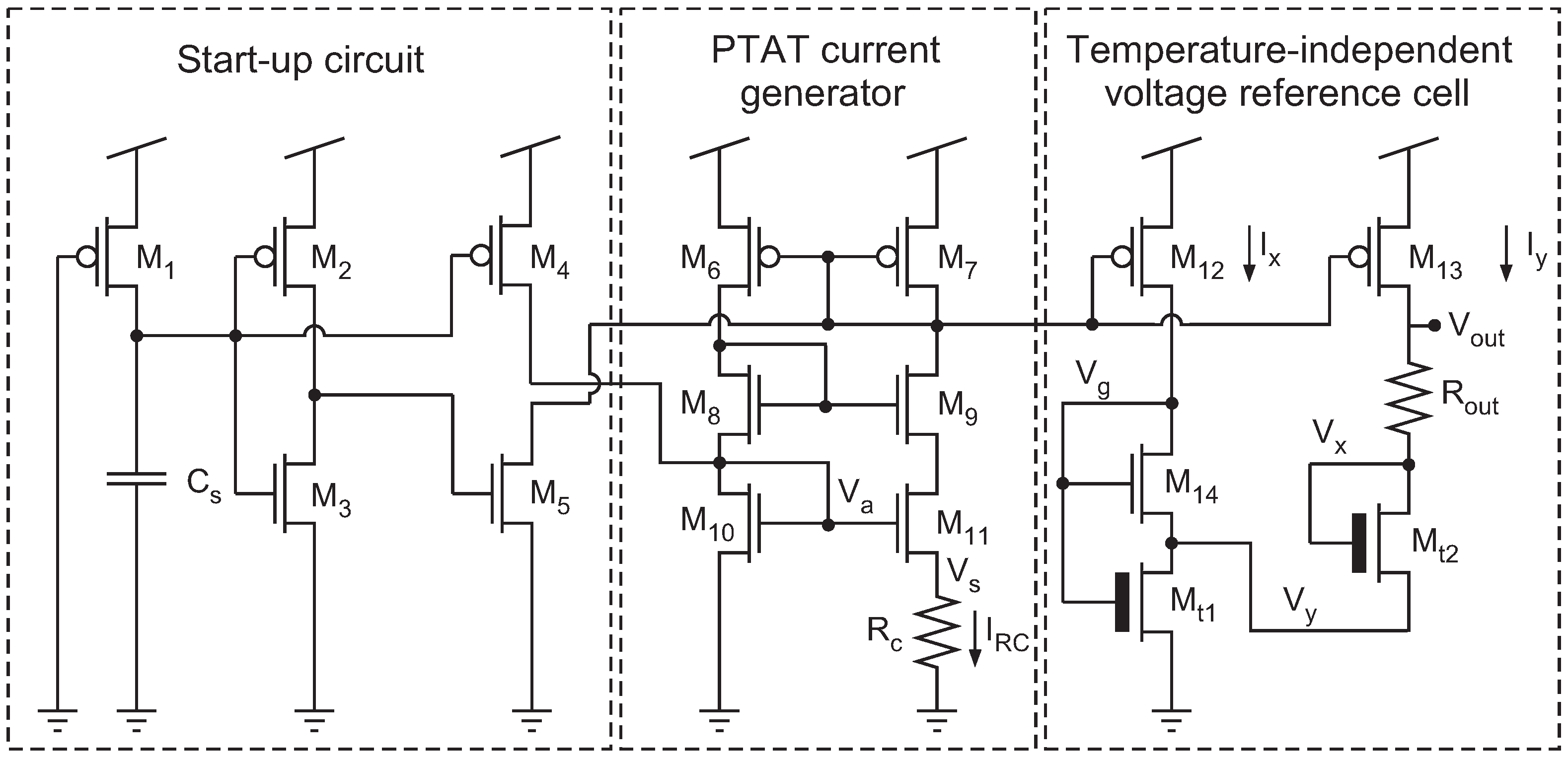
In this section, we present a voltage reference circuit that uses both standard transistors and 5 V I/O transistors to generate a low-TC output voltage while consuming low power. The complete voltage reference circuit is shown in
Figure 1. All the transistors used in this circuit are standard (thin-oxide) transistors except for
and
that are thick-oxide transistors (5 V I/O devices). Two resistors are used in this circuit—one to generate the reference current (
) and the other to generate the final reference voltage (
).
This circuit has three main blocks, as shown in
Figure 1. A current reference cell is used to generate a current that is proportional to absolute temperature (PTAT). A start-up circuit is used to initialize the current reference cell and stabilize its current at a nonzero value. Finally, the third block generates the temperature-independent voltage by first creating a voltage at node
that is complementary to absolute temperature (CTAT). Resistor
then combines the PTAT and CTAT signals into an overall output voltage that has very low temperature dependence.
To achieve low power consumption, our circuit was designed to operate in the subthreshold region with very low bias currents. The drain current of a transistor biased in subthreshold can be expressed as [
17]:
where
,
S is the aspect ratio (
) of the transistor,
is the thermal voltage,
k is the Boltzmann constant,
q is the elementary charge,
T is the absolute temperature in kelvins,
is the MOSFET threshold voltage, and
is the subthreshold slope coefficient representing the capacitive coupling from the gate to the surface potential (
). Voltages
,
, and
are the gate, source, and drain voltages, respectively, referenced to the substrate. When the transistor operates in the saturation region,
approaches zero and is, therefore, negligible. We also assume that the transistors have been designed with large-enough channel lengths that the channel-length modulation effect can be safely neglected.
The detailed operation of each block will be explained in the remainder of this section.
2.1. Reference Current Generator
We use a standard PTAT current generation block that includes a current source and a current mirror. The difference between the
values of
and
establishes a voltage across
. By proper sizing of
,
, and
(
), all the transistors in the PTAT current generator can be biased to be in the subthreshold region. By setting
, the PMOS current mirror provides unity gain. Using Equation (
1) to define expressions for the currents in
and
, the current generated by
is
which linearly increases with temperature.
is mirrored to
and
with ratios of
x and
y. Thus, we have
Accordingly, the voltage drop across
caused by the PTAT current source can be expressed as
This voltage is PTAT and can be set by and the aspect ratios for and .
2.2. Start-Up Circuit
A start-up circuit is used to initialize the current reference cell and stabilize its current at a nonzero value (
). We use the start-up circuit presented by [
18]. This start-up circuit turns on
,
,
, and
at power-up to initialize a nonzero
. After a very short delay,
is charged up to
through
, thereby turning off
and
so that they no longer inject current to the current generator. After the brief initialization period, the start-up circuit consumes no appreciable current and, therefore, does not add to the overall power consumption of the voltage reference cell.
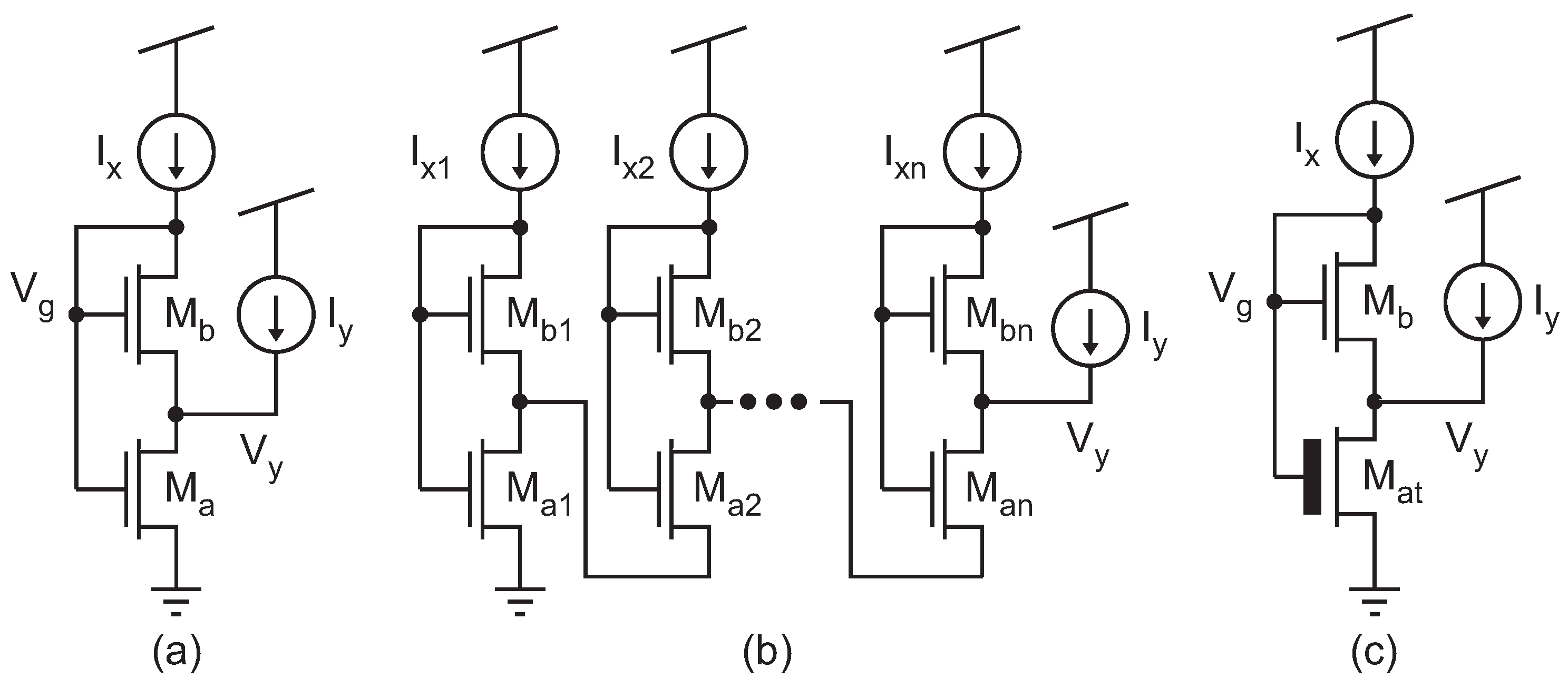
2.3. Temperature-Independent Voltage Reference Cell
The temperature-independent voltage reference cell is based upon a modified version of the building block shown in
Figure 2a that is commonly used as a PTAT voltage generator (e.g., [
19]). The currents through
and
are
and
, respectively. These two currents can be expressed using Equation (
1) as
By dividing Equation (
7) by Equation (
6) and solving for
, we find that
The resulting voltage is PTAT and can be set by proper sizing of
and
and the bias currents (
and
). However, the value of
cannot be made large because of the log compression working on the ratio of the transistor sizes and currents. Some designs stack this circuit repeatedly to generate a higher reference voltage, as shown in
Figure 2b, but they still struggle to achieve a high voltage [
20].
Figure 2c shows a modification to
Figure 2a that replaces the bottom transistor with a thick-oxide device. This configuration has been used previously to provide a low voltage at
that is CTAT [
18,
21,
22]. We, instead, use this configuration to help us achieve a much higher voltage at another node that is also CTAT.
The currents through
and
follow the forms of Equations (
6) and (
7), with the only differences being the various process-dependent parameters for the thick-oxide device,
,
where the extra `t’ in the subscript represents the value for the thick-oxide device. By dividing Equation (
9) by Equation (
3) and solving for
, we obtain
Noting that
and that
, Equation (
10) can be approximated as
with proper sizing of the transistors.
is typically several hundred mV greater than
, which means that using a thick-oxide transistor for
can produce a voltage at
that is much larger than can be produced by
Figure 2a. Additionally,
is dominated by the first two terms of Equation (
11), and since threshold voltages are widely known to be CTAT [
23],
is also a CTAT voltage.
Next, we show that we can use
Figure 2c to create a CTAT voltage at the bottom of
(
) in
Figure 1. The current through
can be expressed as
Using Equations (
11) and (
12), the following equation can be achieved:
Using Equation (
13) and the equation for the current through
, the voltage at node
can be expressed as
where
is dominated by the first two terms of Equation (
14), and, since threshold voltages are widely known to be CTAT [
23],
is a CTAT voltage.
Finally,
is the summation of the PTAT voltage given by Equation (
5) and the CTAT voltage given by Equation (
14):
The goal of this voltage reference cell is to generate an above-1 V output using thick-oxide transistors. The execution of this idea is visible in Equation (
17), where
is a considerable portion of the output voltage. Additionally, the voltage drop across
further increases
. Thus, using the proposed structure, a higher voltage can be achieved by using a small number of transistors and taking advantage of the thick-oxide transistor’s larger threshold voltage.
3. Design Procedure for Low TC
In this section, we discuss how to design this voltage reference circuit to have a low temperature coefficient. By taking the derivative of Equation (
17) with respect to
T, we arrive at an equation for the TC at
:
The
terms, which have a negative value, come from the commonly used expression for the temperature effects on the threshold voltage [
23] given by
where
is a reference temperature, and
T is the temperature of interest. The
terms are generally in the mV/K range, with I/O thick-oxide devices typically having larger values than thin-oxide devices.
Analyzing Equation (
18), we can see that the temperature dependence of the resistors and their exact values have little impact on the TC; assuming both resistors are made from the same material, their temperature dependencies cancel in the first term.
is also contained within the ln term, but its temperature effects have little impact since they are compressed by the logarithmic function; hence, the temperature effects of
are neglected in this analysis (and they are far less significant than the
T term in the same ln function). The
term also contains the temperature-dependent items
,
, and
; again, since they are logarithmically compressed, they have little impact on the overall TC, and their temperature effects can be safely neglected. The only other remaining temperature-dependent term in Equation (
18) is
T within
. Since
T is within an ln function, its effect on the TC is significantly compressed, meaning that it is possible to achieve a low overall TC. To achieve a low TC over a temperature range of interest, a reference temperature in the middle of the range should be chosen; then, the TC can be minimized by setting Equation (
18) equal to zero at that reference temperature,
. By then solving for
and plugging that expression into Equation (
17), we find the optimal value for
:
Noting that the
terms have negative values (i.e.,
is CTAT) and are typically in the mV/K range [
23], the optimal
at room temperature will be greater than 1 V, particularly because of the reasonably high
of 5 V I/O devices. An estimate for
can be calculated from Equations (
20) and (
21) by obtaining values for
,
,
,
,
, and
from the simulation models. Accordingly, for our design,
≈ 1.6 V.
To minimize the TC, the output voltage of this circuit as given by Equation (
17) should be designed to equal
. The use of the resistive ratio
greatly simplifies this design consideration. Once again, we note that the transistor aspect ratios in Equation (
17) are primarily within ln functions, so the ratio of
plays an important factor in establishing the correct
. To determine the best ratio for
to minimize the TC, Equations (
17) and (
20) can be equated, and the best resistor ratio can be found to be
In our design, a ratio of
is needed to achieve a good TC and, accordingly, cause
. Additionally, by changing the resistive ratio slightly, the temperature at which the TC is minimized can be shifted to a higher or lower value while still maintaining a good TC. Of note, our implementation utilized discrete off-chip resistors, limiting our ability to exactly achieve
, and the resulting TC was still low. Varying the resistor ratio is explored further in
Section 4.
Next, we present a design procedure to obtain a low-TC, above-1 V voltage reference cell using the circuit of
Figure 1.
Set , and choose a proper size for to bias the current reference cell in subthreshold. Note that increasing will necessitate a larger in order to bias the circuit in subthreshold, so area limitation requirements for the circuit can be used to set a maximum value of .
Choose appropriate transistor aspect ratios such that
and also that
x and
y keep all transistors in the subthreshold. These design choices make it possible to approximate Equation (
10) with Equation (
11).
Ensure that all transistor lengths are large enough to neglect the effects of channel-length modulation.
Choose the midpoint,
, of the desired temperature range, and use Equation (
22) to solve for
.
If the midpoint of the
vs.
T curve is not at the desired location, then, according to Equation (
22), we can adjust
to move
to higher or lower temperatures. In addition,
must be adjusted, accordingly, to keep the resistive ratio at a reasonable value, based on Equation (
22).
4. Experimental Results
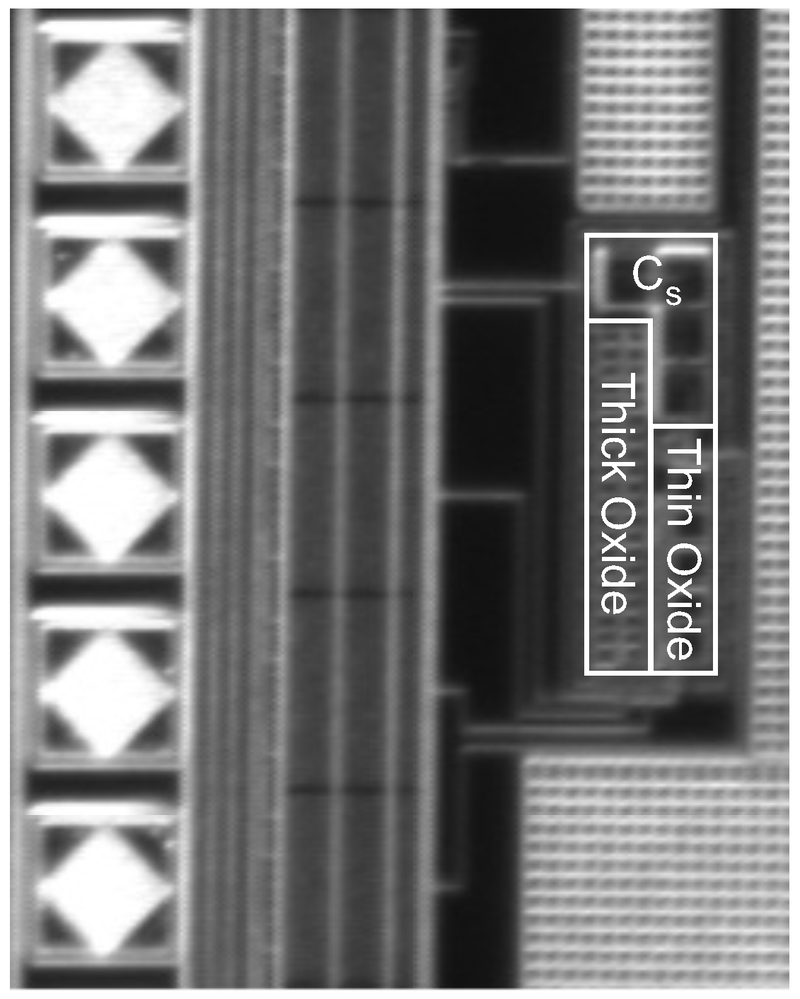
The voltage reference circuit of
Figure 1 was fabricated using a standard 0.35
m CMOS technology and operates on a 3.3 V supply.
Table 1 provides details of the transistor sizes. A die photograph of this circuit is shown in
Figure 3. The die area of this circuit, excluding the resistors, was 0.033 mm
. The resistors (
and
) used in this circuit were off-chip resistors to allow for variety of
combinations. Using the design procedure of
Section 3, we found that
for a low TC output.
and
were set to 3 M
and 500 k
, respectively, to achieve this ratio and to ensure subthreshold operation. These values were also chosen to minimize the TC around room temperature. If the resistors that we used in our experiments were integrated on chip, the die area would increase to 0.06 mm
. Future implementations of this circuit would include on-chip resistors; basic trimming capabilities can be used to modify both the resistor values and resistor ratio to meet the required
and TC. One simple and conventional approach for trimming in a standard CMOS process is to create a series combination of smaller resistor values, each of which can be shorted out through digital selection to achieve the desired resistance.
A Tenney TUJR environmental chamber was used to measure the performance of this circuit under varying temperatures; this environmental chamber has a temperature range of −75
C to 200
C.
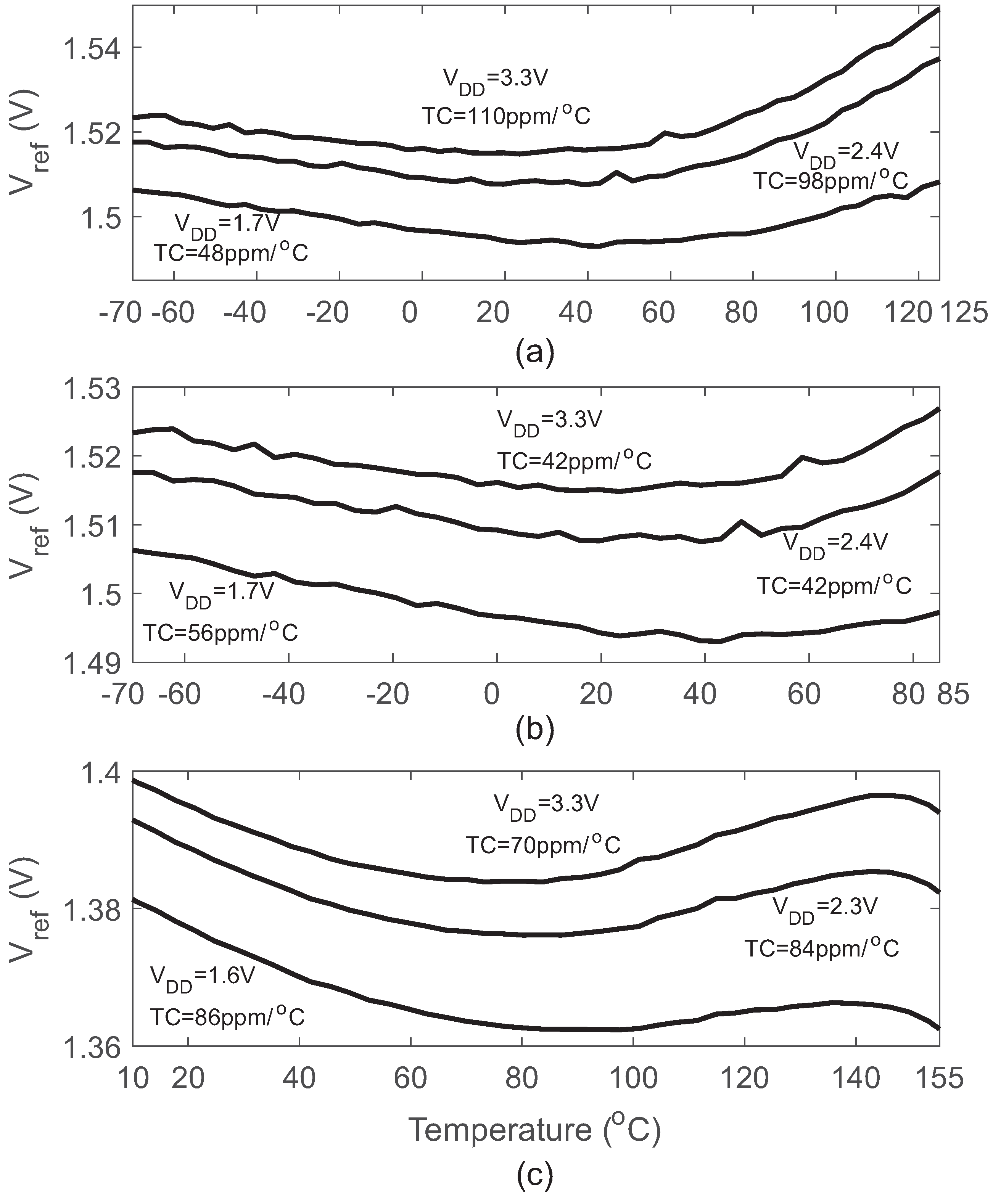
Figure 4a,b shows the measured
over temperature for multiple values of
.
Figure 4b shows that this circuit is able to achieve a low TC of 42 ppm/
C over the temperature range of interest (−70 to +85
C). Even extending this temperature range significantly to cover from −70 to +125
C, this circuit can still achieve a TC of 110 ppm/
C at the nominal
= 3.3 V (see
Figure 4a). By reducing
to 1.7 V, the TC is 48 ppm/
C over this extended temperature range.
As discussed in the previous section, this circuit can be optimized to achieve a good TC for different temperature ranges.
Figure 4c shows an example of shifting the midpoint of the temperature range to a higher value. This midpoint reference temperature can be increased by setting
to a smaller value and by also reducing the value of
, as is evidenced by Equation (
18). In this example,
was reduced to 400 k
, which increases the temperature midpoint,
, due to the
term.
was also decreased to 2 M
to keep the resistor ratio similar (but slightly smaller). The result is that the same circuit, with different resistor values, can be used to provide a low TC (70 ppm/
C at
= 3.3 V) at higher temperatures (+10 to +155
C). Under this condition, the output voltage was
= 1.395 V, and, if the resistors were integrated on-chip, then the area would be 0.044 mm
.
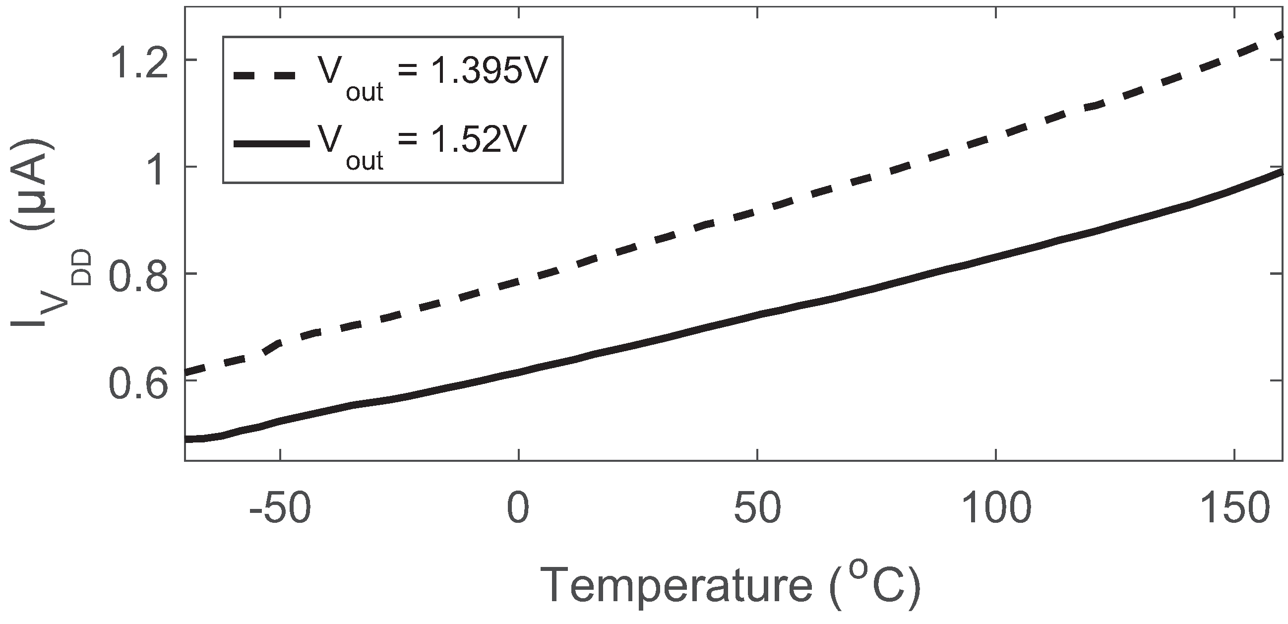
The measured supply current versus temperature for these two reference voltages (
= 1.52 V, 1.395 V) under a
V supply is shown in
Figure 5. The power consumption of this circuit at room temperature for the two
conditions were 1.11
W (
= 1.52 V) and 1.34
W (
= 1.395 V). Thus, this circuit is an appropriate choice for low-power applications.
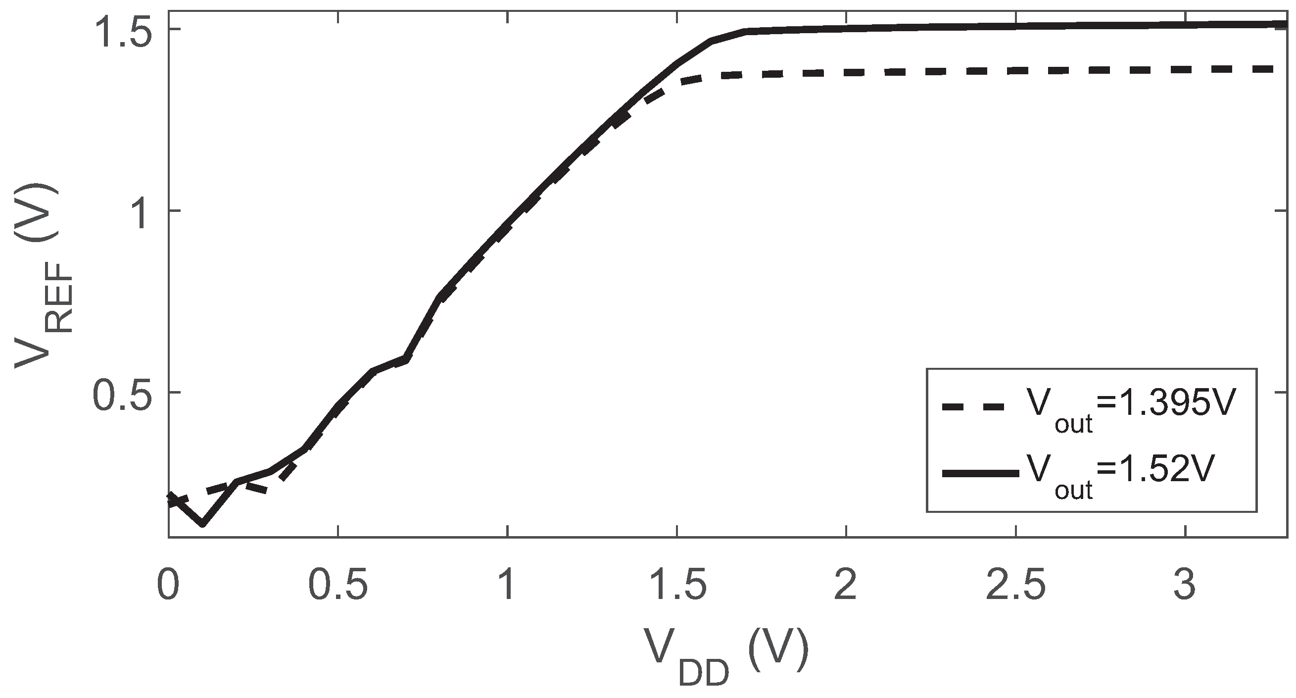
The line regulation of the circuit was measured at room temperature by sweeping the supply voltage from 0 V to 3.3 V, as shown in
Figure 6. The line regulation for the two
conditions of
Figure 4 were 10 mV/V (
= 1.52 V) and 9.3 mV/V (
= 1.395 V). The line regulation can be significantly improved by cascoding the PMOS transistors
,
,
, and
at the expense of a higher minimum supply voltage. Simulation results show that using a cascode structure would improve the line regulation to 2.88 mV/V and would only degrade the supply range by approximately 100 mV. The limited
of this circuit was due to the high output voltage of the circuit. In both
cases,
was approximately
mV (and would be approximately
mV if cascoded PMOS devices were used to improve the line regulation).
The measured power supply rejection ratios (PSRR) at 100 Hz were −35 dB ( = 1.52 V) and −37.9 dB ( = 1.395 V). The PSRR values at 1 MHz were −44 dB ( = 1.52 V) and −44.8 dB ( = 1.395 V).
The die-to-die distribution of the DC output voltage was found at room temperature by measuring the average reference voltage () and the standard deviation () for 17 available chips. The coefficient of variation () for the V and V outputs were and , respectively.
Table 2 compares the three cases of our voltage reference circuit shown in
Figure 4 to other similar circuits. Specifically, we compared our work to other circuits that (1) were fabricated; (2) were in a CMOS process; (3) have
≥ 1 V; and (4) have power consumption ≤50
W. As can be seen from this table, our voltage reference circuit is able to provide a good balance of a low TC, low power consumption, and a large range of temperatures. Additionally, our circuit only uses devices available in standard CMOS processes (thicker-oxide I/O devices are now widely available), whereas some of the listed designs require non-standard devices [
13,
15].


