Article

A Dynamic Current Pulsing Technique to Improve the Noise Efficiency Factor of Neural Recording Amplifiers

Electrical and Systems Engineering, University of Pennsylvania, Philadelphia, PA 19104, USA
*
Author to whom correspondence should be addressed.
J. Low Power Electron. Appl. 2025, 15(4), 67; https://doi.org/10.3390/jlpea15040067 (registering DOI)
Submission received: 20 October 2025 / Revised: 24 November 2025 / Accepted: 28 November 2025 / Published: 1 December 2025

Abstract

Low noise and low power neural recording amplifiers are required for implantable devices measuring action potentials. This paper presents a dynamic current pulsing technique combined with a special type of two-stage low-pass filter (LPF) that demonstrates an improvement in the noise efficiency factor (NEF) beyond that achievable using traditional design. A low NEF of 1.55 is achieved at an average power consumption of 587.8 nW and 5.18 µVrms noise, integrated from 0.1 to 9.8 kHz, inclusive of the impacts of sampling and aliasing. The NEF is improved from 1.76 in the static low current state (LCS) and 1.67 in the static high current state (HCS), measured on the same amplifier chip.

1. Introduction

Acquiring bio-signals in living objects is a method to obtain physiological information for medical purposes. If we classify bio-signals by physical nature, they include electrical, magnetic, thermal and chemical [1]. Bio-electrical signals arise from ions flowing across the membrane of excitable cells, such as neurons and muscle cells. Devices for measuring electrical bio-signals are desired for medical applications where the devices measure the signals with further processing to provide feedback for diagnosis and treatment. Electrical signals produced by the body usually have a small amplitude requiring low noise and low power analog front-end amplifiers and signal processing circuitry.
Among all the bio-electrical signals, studying neural signals is an important field. Neural signals from the brain carry and transmit rich physiological information. These neural activities measured from the brain can be utilized to analyze and treat brain network disorders, such as epilepsy [2,3,4], movement disorders [4,5], schizophrenia [6] and dementia [7]. The electrical signals from the human brain can be classified into different types, based on different acquisition technologies and sources. An electroencephalogram (EEG) is an extracranial technique in which sensors are put onto the scalp to record the neural signals on the brain surface [3]. The EEG signal has a frequency range of less than 100 Hz. Recording from the brain surface using electrodes that are attached to the exposed cortex is called electrocorticography (ECoG) [8]. The target signal has a frequency range of less than 200 Hz. The voltage fluctuation across a single cell’s membrane is called the action potential or neural spike. Spikes occupy the frequency band from about 100 Hz up to 10 kHz. With the action potential, nerves are able to transmit cell-to-cell information rapidly from one part of the body to another. Implantable devices with brain-penetrating electrodes can record neural information such as spikes and low field potentials (LFP) [4]. The neural recording amplifier is the front-end amplifier for this technology. Then, machine learning algorithms can be applied to the amplified signals to analyze the neural activities [9,10,11,12,13]. For example, “spike sorting” refers to an algorithm to classify spikes produced by multiple neurons from which the electrode records simultaneously [10,11,12,13]. Usually, the spike shape and amplitude from a single neuron is unique and affected by the position with respect to the recording electrodes. To isolate the signal from each single neuron would help us to understand the electrophysiological mechanisms in the field of neuroscience.
A neural recording amplifier is required to have low noise and small size to measure individual neuron activity. This implantable device should also have low power consumption, so dissipated heat will not destroy the brain tissue, allowing for simultaneous recording from a large number of channels [14,15]. Improving the NEF [16,17,18] of neural recording amplifiers through the tradeoff between the power and noise for transistors in integrated circuit (IC) design is an important research area. The NEF is defined by Equation (1):
N E F = V n i , r m s   2 I s u p p l y π · U T · 4 k T · B W
where V ni , rms is the input-referred voltage noise of the neural recording amplifier in rms over the bandwidth, I s u p p l y is the supply current consumed in the amplifier, U T is the thermal voltage k T q , k is Boltzmann’s constant and B W is the bandwidth of the neural recording amplifier. Prior research reduced the NEF via innovative techniques such as dynamic range folding, chopper stabilization and inverter stacking [17,19,20,21].
A traditional neural recording amplifier [15,22] usually has the structure shown in Figure 1, which was first published in Olsson [23]. The AC coupling structure is utilized to solve the dc-baseline stabilization problem, which arises from the potential difference between the recording electrode and the extracellular electrolyte [24]. This DC potential can be as large as 250 mV and would drift gently over a range of tens of mV [24], which could destroy the dynamic range of the recording amplifier if this DC polarization drift is not eliminated from the acquisition. The high-pass (HP) corner should be less than 100 Hz to record action potentials and 10 Hz to record LPF, and has the following expression:
f 3 d B = 1 2 π R f C f
R f is implemented as a pseudo-resistor, utilizing the diode-connected back-to-back transistors to achieve a resistance > 1 GΩ [15,22]. Low input noise is required to record action potentials with amplitudes < 50 µV. The input-referred voltage noise of this closed-loop structure is as follows [22]:
v n i C L 2 ¯ =   v n i O L 2 ¯ C i n + C f + C i n o p a m p C i n 2
where v n i O L 2 ¯ is the open-loop input-referred voltage noise of the operational amplifier (OPAMP) and C i n o p a m p is the input capacitance of the OPAMP.
This work introduces a dynamic current pulsing technique to improve the power consumption/noise tradeoff in the design of neural recording amplifiers. Most previous research on neural recording amplifiers operates under constant power consumption [15,16]. Mondal [25] implemented current pulsing to switch slowly or reconfigure between a HCS and a LCS, for example, to reconfigure the power consumption based on the input signal characteristics. Here, we explore dynamically changing between noise states within a sampling period to improve NEF, where the pulsing rate is much faster than the frequency of neural activity. Xiao [26] implemented similar techniques to modulate the current of a neural amplifier in order to reduce power consumption and noise. In contrast, in this work we carefully investigate the modulation/switching frequencies and duty cycles of high-current and low-current states, enabling an optimized balance between noise and power. We achieve a significantly lower NEF compared to that reported in [26].
The dynamic current pulsing alters the circuit power consumption and noise performance, as depicted in Figure 1. The amplifier in Figure 1 is pulsed into the HCS for a short amount of time and stays in the LCS for the rest of the cycle, thus dynamically altering the output noise, as depicted in Figure 1. The output voltage should be sampled where the noise is at a minimum, at the end of the HCS. A fast settling is required for both the signal and noise when the transition from the LCS to HCS occurs. In addition, noise folding arising from aliasing can corrupt the noise performance if the overall sampling architecture is not optimized.
This paper presents a neural recording amplifier applying the current pulsing technique with post-processing to achieve a NEF of 1.55, inclusive of the impact of sampling and aliasing. The reported ASIC has a power consumption of 587.8 nW, with an input-referred voltage noise of 5.18 µVrms, integrated over a 100 Hz to 9.8 kHz bandwidth. The NEF is significantly improved when compared to constant operation in either the HCS or LCS.
Section 2 details the neural recording amplifier implementation. The performance of the application-specific integrated circuit (ASIC) is presented in Section 3. Section 4 introduces the post-processing that is applied to the ASIC measurement and the improvement in the noise performance of the reported neural recording amplifier.

2. Circuit Design

2.1. Current Pulsing Technique

By applying a current pulsing technique, the amplifier’s average current and power can be reduced. The average current consumed in the pulsing condition can be expressed as follows:
I p u l s e = I H 1 D L + I L D L
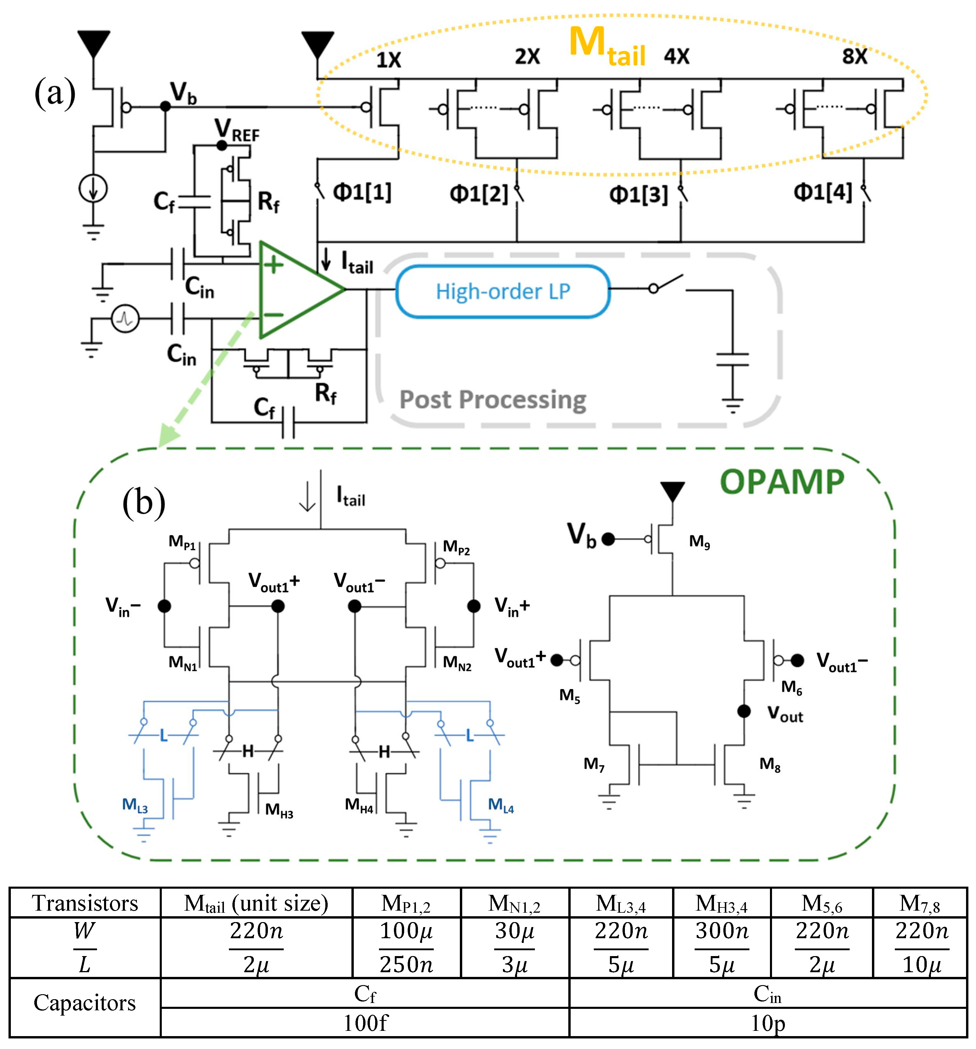
where I H and I L are the supply current of the HCS and the LCS, respectively and D L is the duty-cycle of the LCS. Following the tradeoff between the current and the thermal noise of the MOSFET, the LCS is the high-noise state and the HCS is the low-noise state. By sampling the voltage at the end of the HCS, a low noise level approaching that of the HCS can be realized, as depicted in the right of Figure 1. Here, the pulsing frequency, f p u l s e , is the same as the sampling frequency, f s a m p l e . Figure 2a illustrates the implementation of a neural recording amplifier employing the pulsing technique with transistor-level details. The pseudo resistors and capacitor in feedback form an HP pole [22,27] and this gives a corner frequency of 5.6 Hz, according to the TSMC 180 nm spectre simulation. Switches 1 ,   2 ,   3 ,   4 control the tail current coming out of the current mirror, which achieves the HCS and LCS. Each branch has 1×, 2×, 3× and 4× transistors in parallel, in order to program the current, I t a i l , coming from Mtail. The OPAMP, as shown in Figure 2b, has two stages. We switch at a constant frequency that is not connected to the input. As a result, the charge injection appears as a fixed, periodic component at the switching frequency, which lies outside the input band of interest. A fully differential amplifier is utilized in the first stage to reject the common-mode DC voltage fluctuation introduced by changing the tail current. The current reuse structure [16,28], utilizing MP1, MN1, MP2 and MN2, is chosen to boost the transconductance, which benefits the noise performance and the power consumption. Transistors M3 and M4 are used for the output common-mode feedback (CMFB) for this fully differential stage, as shown in Figure 2b. There are two pairs of transistors implementing M3 and M4. MH3 and MH4 and ML3 and ML4 utilize different dimensions and are designed for the HCS and LCS, respectively. When the common mode (CM) of outputs Vout1+ and Vout1− rises, M3 and M4 increase the tail current in both branches. To supply this higher current, PMOS transistors MP1 and MP2 drive the output nodes to a lower voltage, thereby pulling the common mode down towards its target. The opposite occurs if the CM output voltage falls, thereby setting the CM output voltage using the feedback current provided by M3 and M4. Switching in and out each pair, MH3 and MH4 or ML3 and ML4, helps to rapidly stabilize the output DC operating points of the first stage when current switching occurs. As the second stage is a single-ended output amplifier, which has a lower common mode rejection ratio, the stabilization of the input DC voltage allows for much faster settling at the output. The HCS current bias is selected to satisfy the input-referred noise requirements. The LCS current is minimized but the transistors should remain in a safe operation region. The simulation results indicate that the HP corner frequency lies at 6 Hz under the pulsing operation, which is consistent with the steady-state performance. The total harmonic distortion (THD) is 2.1% for a 500 µVPP sinusoidal input, corresponding to the maximum neural spike amplitude, when sampling at the end of the HCS at a 50 kHz pulsing rate. The THD is identical to that in steady-state operation, demonstrating that the amplifier has good settling behavior and pulsing the amplifier does not distort the input signal. After the front-end amplifier, a high-order LPF and a sampler are applied using post processing.

2.2. Settling Time and Noise Folding

The faster the signal and noise settle in the HCS, the larger the percentage of time the amplifier can stay in the LCS and the more the NEF can be improved by our pulsing technique. A small RC time constant, corresponding to a large small-signal bandwidth, in conjunction with transistors MH3, MH4, ML3 and ML4, allows for fast settling of the signal and noise when the LCS to HCS transition occurs. Even though the output DC voltage is designed to match between the LCS and HCS, considering the process, voltage and temperature variations, as the current is switching between the LCS and HCS, there is a larger DC operating point variation when compared to the neural signal amplitude at the output of the first stage of the amplifier and this limits the overall amplifier settling time. Thus, the bandwidth of the first stage in Figure 2b should be large compared to the pulsing rate to allow for fast settling. The bandwidth of the HCS is of critical importance, as the noise will be measured at the end of the HCS. However, power consumption is determined by the noise requirements and this power results in a large bandwidth for the first stage of 450 kHz in the HCS. Equation (5) shows the settling of Vout1 from the initial voltage at the end of the LCS, V l , to the final HCS value, Vh, for a given time constant, τ .
v o u t 1 t = V h V l V h e t τ
To achieve a 0.1% settling residual, ensuring that transient residuals remain at least 60 dB below the signal level, for a bandwidth of 450 kHz, the settling time is 2.44 μ s . This results in the first stage having good settling behavior, even when pulsing at 200 kHz. In the LCS operating current, the higher output resistance of transistors limits the first-stage bandwidth to 150 kHz. The dominant pole of the amplifier lies in the second stage.
The voltage at the output of the amplifier that is required to settle includes the DC voltage, the AC signal and noise. Ensuring the same DC operating points for the low/high current states and a large bandwidth for the first stage allows for the DC voltage at the output to remain minimally changed upon current pulsing. This also benefits from the fully differential structure of the first stage and MH3, MH4, ML3 and ML4 in Figure 2b. The AC signal is the amplification of the neural signal, which has small amplitude and is within the bandwidth of the amplifier. The low frequency noise has the same properties as the AC signal. The settling of the AC signal and noise within the neural bandwidth are not of concern with a proper design. However, the high frequency noise outside the amplifier bandwidth has difficulty in settling rapidly. Thus, fast settling of the noise desires a high amplifier bandwidth.
Increasing the amplifier bandwidth reduces the RC time constant, τ . Smaller τ reduces the settling time based on the simplified RC settling in Equation (5). In conflict with the high amplifier bandwidth desired for fast noise settling, the noise beyond the Nyquist frequency, f s /2, is folded into the bandwidth after the sampling process. The higher the bandwidth, the more noise outside of f s /2, so more noise will be aliased to the signal band after the sampling. Therefore, there is a tradeoff between the aliased noise and settling time, based on the filter bandwidth and implementation. Typically, an anti-aliasing filter is required before the sampling to pre-filter the noise outside f s /2 and maintain the signal-to-noise ratio after the sampling. A high-order LPF with a bandwidth of approximately f p u l s e , placed after the front-end amplifier but before the sampling, can filter the high frequency noise as much as possible, while still allowing for fast settling time. Oversampling here implies a high pulsing rate and high sampling rate, further reducing the noise aliasing. Oversampling allows for the anti-aliasing filter to be implemented with a larger bandwidth, which in turn allows for faster noise settling.
In Section 3 and Section 4, different LPFs have been applied after the amplifier to investigate the parameters of the LPF that achieve the best NEF. Low power anti-aliasing filters are required for both pulsed and steady-state neural recording amplifiers to prevent aliased noise from sampling ADCs. High-order low-pass filters can be realized with low power consumption using active Gm-C filters [29,30]. In a Gm-C filter, the resistor elements of a classical RC ladder are replaced by transconductance, allowing for the pole frequencies to be set by the ratio G m 2 π C . This makes the cutoff frequency both tunable and highly compatible with ultra-low-power operation, since Gm can be adjusted with sub-nanoamp bias currents in weak inversion or subthreshold.

3. ASIC Measurement

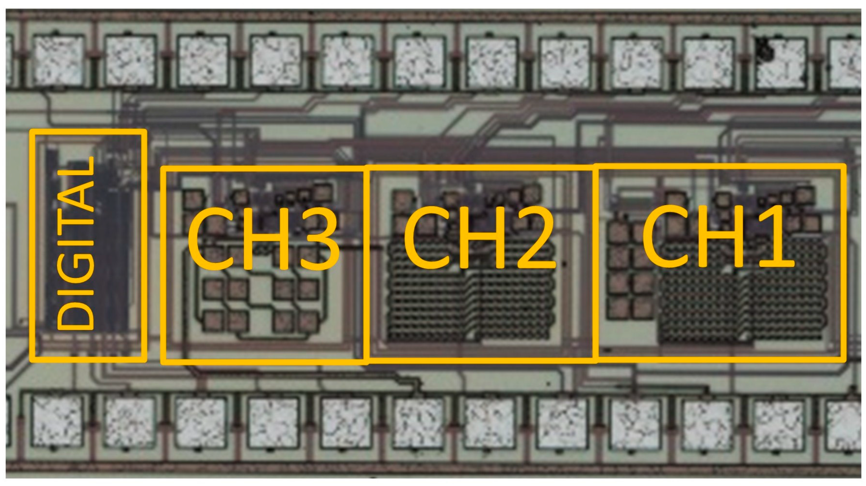
The chip layout and micrograph are shown in Figure 3.
The amplifier is implemented in the TSMC 180 nm CMOS process with VDD = 1 V. A National Instruments acquisition device (NI DAQ, National Instruments Corporation, Austin, TX, USA) 6221 is used to provide the clock for controlling switches 1 ,   2 ,   3 ,   4 . The output of the chip is recorded using a NI DAQ with a sampling rate of 250 ksps. The HCS and LCS consume 1.054 µA and 277 nA, respectively. The measured 3 dB bandwidth of the amplifier on the chip is 39 kHz. The noise and transfer function are measured in the HCS and LCS, and under dynamic current pulsing. The input-referred noise spectral density of the LCS and HCS are shown in Figure 4. The average noise spectral density from 100 Hz to 10 kHz in the LCS and HCS are 80.8 nV/√Hz and 43.9 nV/√Hz, respectively. The 1/ f corner frequency is approximately 300 Hz. The time domain output data from the chip in the dynamic pulsing condition is shown in Figure 5. The output is dynamically switching between the LCS and HCS, as the LCS and HCS have a slightly different offset voltage. The pulsing occurs outside the action-potential bandwidth, so pulse-induced artifacts can be filtered out without degrading the neural signal’s transient information. This does not affect the transfer function in the pulsing condition, as shown in Figure 6. To achieve the best NEF, different pulsing frequencies, f p u l s e , and pulsing clock duty cycles, D L , that are applied to the chip are studied. The recorded output noise was imported to MATLAB 2021b. A first-order LPF with different corner frequencies was applied to the data to study the bandwidth effect on the noise settling. The data were subsequently down-sampled to f p u l s e . Figure 7 shows the result for f p u l s e = 25   k H z and f p u l s e = 50   k H z . The pulsing duty cycle of the LCS, D L , is 20%, 40%, 60% and 80%, as shown in the legend. The results for the steady-state HCS and LCS when applying the same LPF are also included in the figure in order to show the advantage of the pulsing technique. The rms input-referred noise integrated within the bandwidth and the NEF based on Equation (1) are calculated. The supply current in the pulsing condition is calculated based on Equation (4).
As shown in Figure 7a,b, when pulsing at 25 kHz with sufficient settling duration, applying the current pulsing technique achieves a large improvement in NEF compared to operating exclusively in the HCS or LCS. However, sampling at 25 ksps introduces a large amount of noise folding. When pulsing at 50 kHz, a narrow-bandwidth LPF averages the noise without enough time for the noise to settle during the HCS. Based on the results in Figure 7, a duty cycle of 40% and 60% in the LCS with a pulsing rate of 50 kHz is chosen for further study, as these conditions have the lowest NEF with the widest filter bandwidth.

4. Post Processing

4.1. Sample-and-Hold Filter

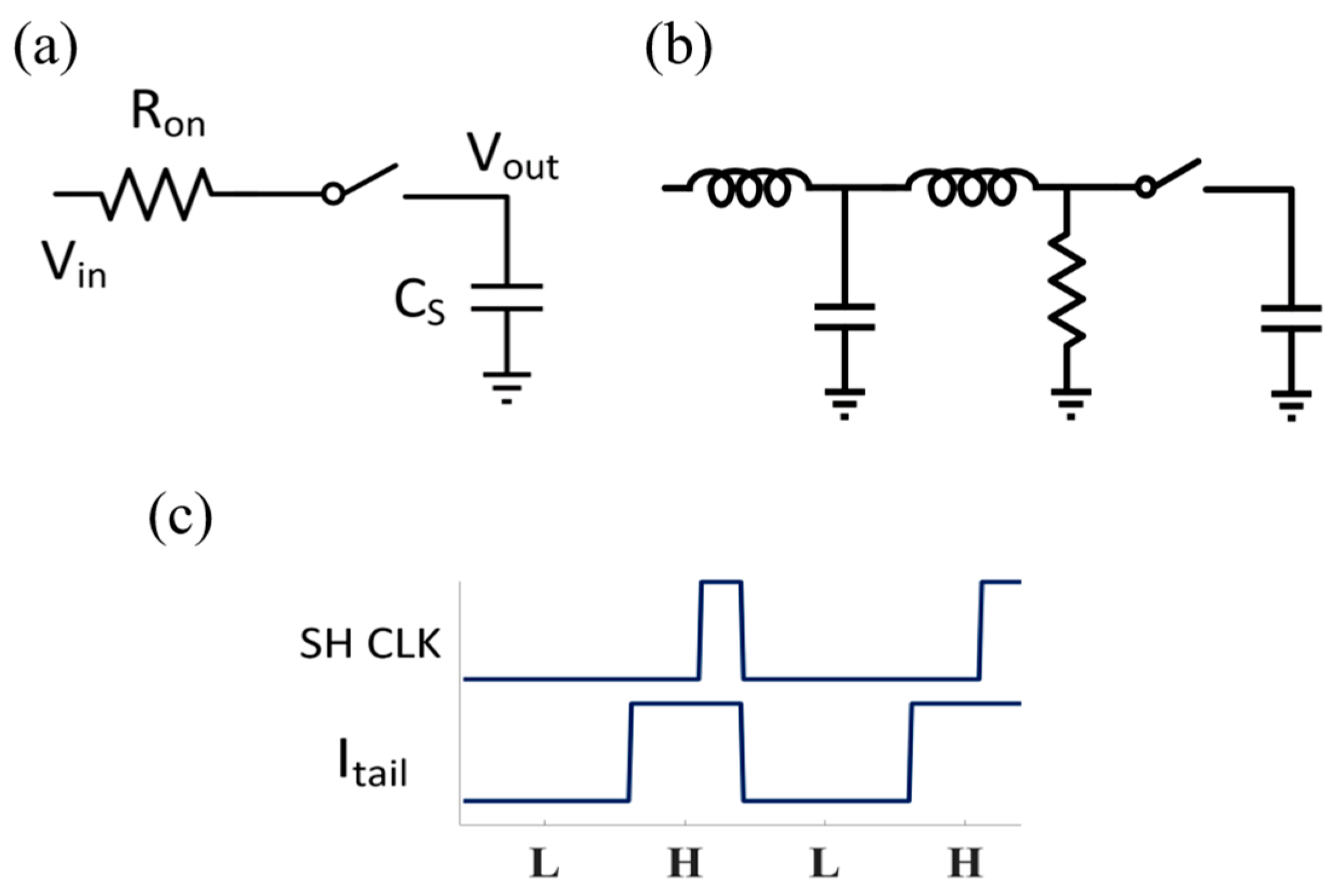
To improve the NEF when sampling at 50 ksps, a high-order LPF with a large bandwidth should be utilized to filter the high frequency noise. Furthermore, a special type of LPF is introduced, which is implemented using a sample-and-hold structure (SH) as shown in Figure 8a. The SH has a transfer function with a narrow bandwidth but a peak in the response at integer multiples of the sampling frequency, as shown in Figure 9a [31]. If the sampling frequency is the same as the pulsing frequency, and the sampling switch is only on at the end of the low noise state, the high noise from the LCS will not integrate on the sampling capacitor. This structure has a faster settling time than a conventional LPF. The bandwidth of this structure is related to the SH parameters, such as the R o n of the switch, the sampling capacitor value and the sampling duration. A high-order LPF can be implemented as a second-order analog LC filter or a digital filter. Combined with the SH filter, this two-stage LPF has the response shown in Figure 9b and can be designed to have a bandwidth of 10 kHz by tuning the SH parameters.

4.2. Noise Performance

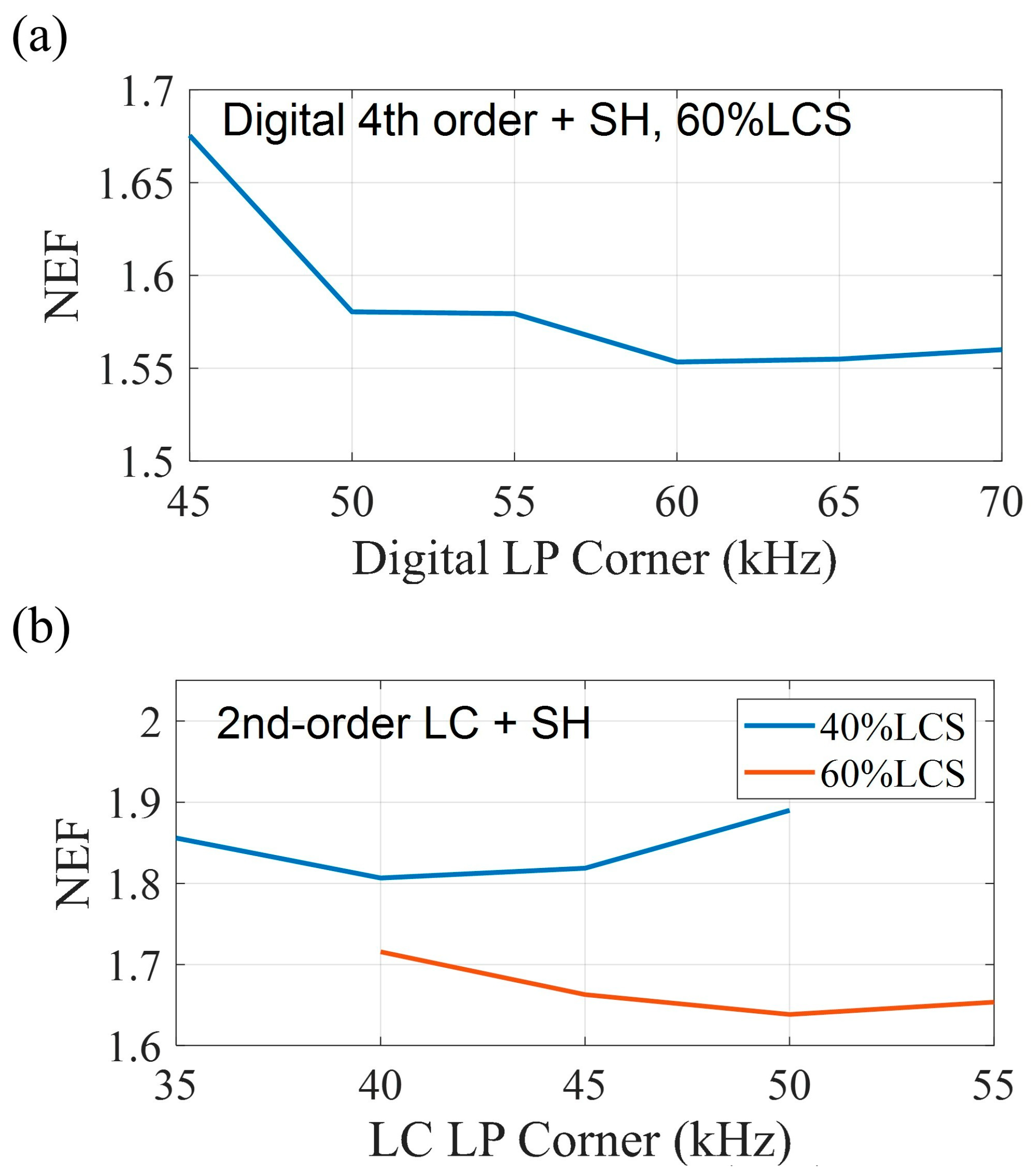
To further study this concept, the SH structure was implemented in Cadence. The timing requirements of the sampling clock and tail current controlling clock are shown in Figure 8c. The sampling switch should turn off prior to the transition from the HCS to the LCS in order not to sample the higher noise from the LCS onto the sampling capacitor. A digital fourth-order LPF as the first stage high-order filter was applied to the data sampled at 250 ksps, which was measured from the chip and imported into Cadence for further filtering from the SH. The lowest NEF of 1.55 is achieved when the high-order LPF has a corner at 60 kHz and a pulsing duty cycle of 60% in the LCS, as shown in Figure 10a. This could be implemented on the chip in the future using a high sample rate analog-to-digital converter (ADC) and digital signal processing (DSP). The input-referred noise performance in this case is shown in Figure 11. The average noise is 52.7 nV/√Hz over a 100 Hz to 9.8 kHz bandwidth, with an integrated input-referred noise of 5.18 µVrms. Compared to the LCS noise and HCS noise in Figure 11, the noise in the pulsing condition is close to the HCS noise, except the noise at the higher frequency is slightly larger. Alternatively, working towards an analog integrated circuit version, a second-order LC filter with −60 dB/dec has also been implemented in Cadence, followed by the SH structure as shown in Figure 10b. By optimizing the LC filter bandwidth to 50 kHz and with a pulsing duty cycle of 60% in the LCS, a NEF of 1.64 is achieved. The second-order low pass filter can be implemented by an active filter on the chip [29,30].

5. Conclusions

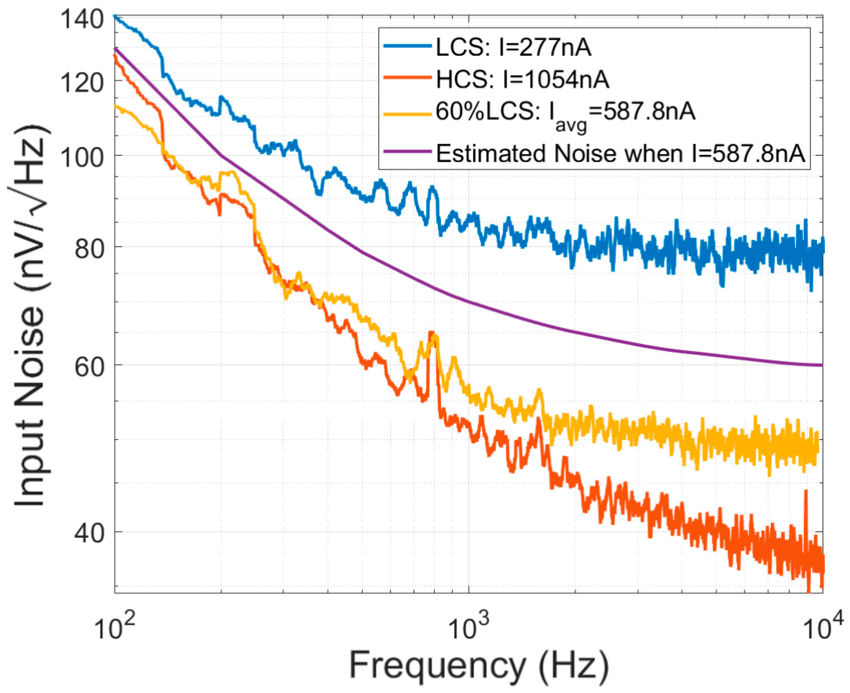
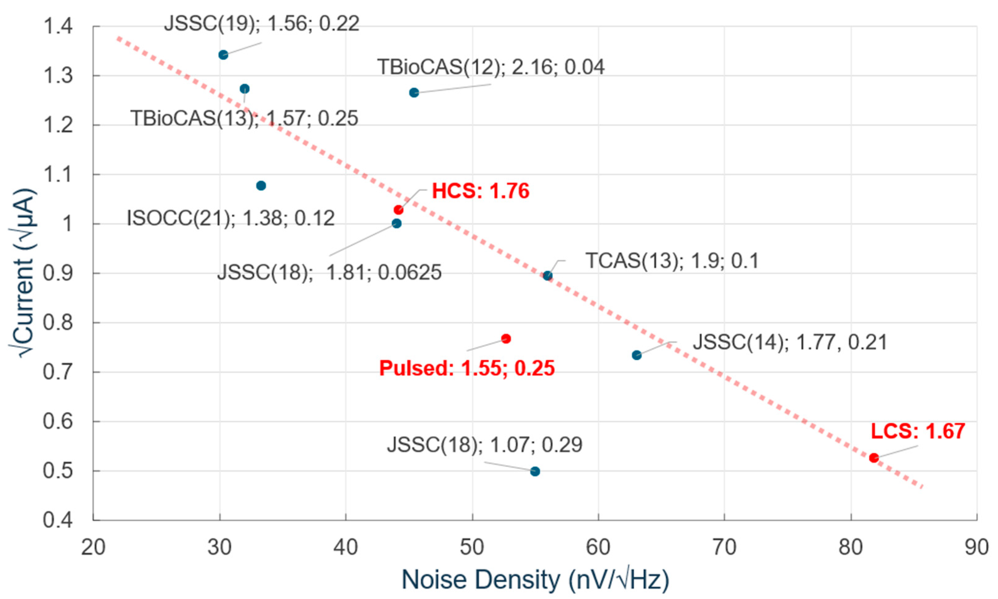
Figure 12 summarizes this research, along with state-of-the-art neural recording amplifiers [16,17,19,20,32,33,34]. When filtering to a 3 dB bandwidth of 10 kHz with a digital fourth order filter and down-sampling to 50 ksps, the pure HCS and LCS in this work achieve a NEF of 1.76 and 1.67 respectfully. By employing the current pulsing technique with optimized filtering, the NEF is improved to 1.55 while maintaining a 9.7 kHz 3 dB bandwidth and a 587.8 nW power consumption, with an input-referred voltage noise of 5.18 µVrms. The noise reported in this work also includes sampling and aliasing and is still among the lowest NEF amplifiers reported. Some works listed in Figure 12 do not include aliased noise, which would be present in any system where an ADC follows the neural recording amplifier. In addition, the trend line in the figure can describe the tradeoff between the noise and the power consumption. Only this work with the dynamic pulsing technique and the papers by Shen et al. [20] and Choi et al. [33] in Figure 12 break away from this trend line. Based on this trend line, the theoretical calculation of the noise with the same power as the 60% LCS pulsing condition but with a constant tail current is shown with the purple line in Figure 11. This illustrates that the proposed dynamic pulsing technique exceeds the limits imposed by Equation (1). In the future, the filter could be realized on the chip and faster pulsing may enable a further reduction in aliased noise. Furthermore, the dynamic current pulsing technique can be applied to other neural recording amplifiers or in other applications to improve the tradeoff between power consumption and noise.

Author Contributions

Conceptualization, R.H.O.III; methodology, R.H.O.III and Y.H.; software, Y.H.; validation, Y.H.; formal analysis, R.H.O.III and Y.H.; investigation, Y.H.; resources, R.H.O.III and Y.H.; data curation, Y.H.; writing—original draft preparation, Y.H.; writing—review and editing, R.H.O.III and Y.H.; visualization, Y.H.; supervision, R.H.O.III; project administration, R.H.O.III; funding acquisition, R.H.O.III. All authors have read and agreed to the published version of the manuscript.

Funding

This research received no external funding.

Institutional Review Board Statement

Not applicable.

Informed Consent Statement

Not applicable.

Data Availability Statement

The original contributions presented in this study are included in the article. Further inquiries can be directed to the corresponding author.

Conflicts of Interest

The authors declare no conflicts of interest.

References

  1. Dey, N.; Ashour, A.S.; Mohamed, W.S.; Nguyen, N.G. Biomedical Signals. In Acoustic Sensors for Biomedical Applications; Springer International Publishing: Cham, Switzerland, 2019; pp. 7–20. [Google Scholar]
  2. Qian, C.; Parramon, J.; Sanchez-Sinencio, E. A Micropower Low-Noise Neural Recording Front-End Circuit for Epileptic Seizure Detection. IEEE J. Solid-State Circuits 2011, 46, 1392–1405. [Google Scholar] [CrossRef]
  3. Thakor, N.V. Translating the Brain-Machine Interface. Sci. Transl. Med. 2013, 5, 210ps17. [Google Scholar] [CrossRef]
  4. Das, R.; Moradi, F.; Heidari, H. Biointegrated and Wirelessly Powered Implantable Brain Devices: A Review. IEEE Trans. Biomed. Circuits Syst. 2020, 14, 343–358. [Google Scholar] [CrossRef] [PubMed]
  5. Chen, K.-H.S.; Chen, R. Principles of Electrophysiological Assessments for Movement Disorders. J. Mov. Disord. 2020, 13, 27–38. [Google Scholar] [CrossRef] [PubMed]
  6. Dvey-Aharon, Z.; Fogelson, N.; Peled, A.; Intrator, N. Schizophrenia detection and classification by advanced analysis of EEG recordings using a single electrode approach. PLoS ONE 2015, 10, e0123033. [Google Scholar] [CrossRef]
  7. Ieracitano, C.; Mammone, N.; Hussain, A.; Morabito, F.C. A Convolutional Neural Network based self-learning approach for classifying neurodegenerative states from EEG signals in dementia. In Proceedings of the 2020 International Joint Conference on Neural Networks (IJCNN), Glasgow, UK, 19–24 July 2020; pp. 1–8. [Google Scholar]
  8. Curot, J.; Busigny, T.; Valton, L.; Denuelle, M.; Vignal, J.-P.; Maillard, L.; Chauvel, P.; Pariente, J.; Trebuchon, A.; Bartolomei, F.; et al. Memory scrutinized through electrical brain stimulation: A review of 80 years of experiential phenomena. Neurosci. Biobehav. Rev. 2017, 78, 161–177. [Google Scholar] [CrossRef]
  9. Bârzan, H.; Ichim, A.-M.; Mureşan, R.C. Machine Learning-Assisted Detection of Action Potentials in Extracellular Multi-Unit Recordings. In Proceedings of the 2020 IEEE International Conference on Automation, Quality and Testing, Robotics (AQTR), Cluj-Napoca, Romania, 21–23 May 2020; pp. 1–5. [Google Scholar]
  10. Xu, H.; Han, Y.; Han, X.; Xu, J.; Lin, S.; Cheung, R.C.C. Unsupervised and real-time spike sorting chip for neural signal processing in hippocampal prosthesis. J. Neurosci. Methods 2019, 311, 111–121. [Google Scholar] [CrossRef]
  11. Chen, Y.; Yang, X.; Gielen, G.; Mora Lopez, C. Optimizing Neural Recording Front-Ends Toward Enhanced Spike Sorting Accuracy in High-Channel-Count Systems. IEEE Trans. Neural Syst. Rehabil. Eng. 2025, 33, 2180–2191. [Google Scholar] [CrossRef]
  12. Saeed, M.; Khan, A.A.; Kamboh, A.M. Comparison of Classifier Architectures for Online Neural Spike Sorting. IEEE Trans. Neural Syst. Rehabil. Eng. 2017, 25, 334–344. [Google Scholar] [CrossRef]
  13. Hao, H.; Chen, J.; Richardson, A.; Van der Spiegel, J.; Aflatouni, F. A 10.8 µW Neural Signal Recorder and Processor With Unsupervised Analog Classifier for Spike Sorting. IEEE Trans. Biomed. Circuits Syst. 2021, 15, 351–364. [Google Scholar] [CrossRef]
  14. Marblestone, A.H.; Zamft, B.M.; Maguire, Y.G.; Shapiro, M.G.; Cybulski, T.R.; Glaser, J.I.; Amodei, D.; Benjamin Stranges, P.; Kalhor, R.; Dalrymple, D.A.; et al. Physical principles for scalable neural recording. Front. Comput. Neurosci. 2013, 7, 137. [Google Scholar] [CrossRef] [PubMed]
  15. Olsson, R.H.; Buhl, D.L.; Sirota, A.M.; Buzsaki, G.; Wise, K.D. Band-tunable and multiplexed integrated circuits for simultaneous recording and stimulation with microelectrode arrays. IEEE Trans. Biomed. Eng. 2005, 52, 1303–1311. [Google Scholar] [CrossRef] [PubMed]
  16. Zou, X.; Liu, L.; Cheong, J.H.; Yao, L.; Li, P.; Cheng, M.-Y.; Goh, W.L.; Rajkumar, R.; Dawe, G.S.; Cheng, K.-W.; et al. A 100-Channel 1-mW Implantable Neural Recording IC. IEEE Trans. Circuits Syst. I Regul. Pap. 2013, 60, 2584–2596. [Google Scholar] [CrossRef]
  17. Han, D.; Zheng, Y.; Rajkumar, R.; Dawe, G.S.; Je, M. A 0.45 V 100-Channel Neural-Recording IC With Sub-μW/Channel Consumption in 0.18 μm CMOS. IEEE Trans. Biomed. Circuits Syst. 2013, 7, 735–746. [Google Scholar] [CrossRef]
  18. Steyaert, M.S.J.; Sansen, W.M.C. A micropower low-noise monolithic instrumentation amplifier for medical purposes. IEEE J. Solid-State Circuits 1987, 22, 1163–1168. [Google Scholar] [CrossRef]
  19. Luo, D.; Zhang, M.; Wang, Z. A Low-Noise Chopper Amplifier Designed for Multi-Channel Neural Signal Acquisition. IEEE J. Solid-State Circuits 2019, 54, 2255–2265. [Google Scholar] [CrossRef]
  20. Shen, L.; Lu, N.; Sun, N. A 1-V 0.25-μW Inverter Stacking Amplifier With 1.07 Noise Efficiency Factor. IEEE J. Solid-State Circuits 2018, 53, 896–905. [Google Scholar] [CrossRef]
  21. Mondal, S.; Hall, D.A. An ECG chopper amplifier achieving 0.92 NEF and 0.85 PEF with AC-coupled inverter-stacking for noise efficiency enhancement. In Proceedings of the 2017 IEEE International Symposium on Circuits and Systems (ISCAS), Baltimore, MD, USA, 28–31 May 2017; pp. 1–4. [Google Scholar]
  22. Harrison, R.R.; Charles, C. A low-power low-noise cmos for amplifier neural recording applications. IEEE J. Solid-State Circuits 2003, 38, 958–965. [Google Scholar] [CrossRef]
  23. Olsson, R.H.; Gulari, N.; Wise, K.D. Silicon neural recording arrays with on-chip electronics for in-vivo data acquisition. In Proceedings of the 2nd Annual International IEEE-EMBS Special Topic Conference on Microtechnologies in Medicine and Biology, Madison, WI, USA, 2–4 May 2002; pp. 237–240. [Google Scholar]
  24. Bai, Q.; Wise, K.D. Single-unit neural recording with active microelectrode arrays. IEEE Trans. Biomed. Eng. 2001, 48, 911–920. [Google Scholar] [CrossRef]
  25. Mondal, S.; Hsu, C.-L.; Jafari, R.; Hall, D.A. A Dynamically Reconfigurable ECG Analog Front-End With a 2.5× Data-Dependent Power Reduction. IEEE Trans. Biomed. Circuits Syst. 2021, 15, 1066–1078. [Google Scholar] [CrossRef]
  26. Xiao, Z.; Tang, C.-M.; Dougherty, C.M.; Bashirullah, R. A 20µW neural recording tag with supply-current-modulated AFE in 0.13 µm CMOS. In Proceedings of the 2010 IEEE International Solid-State Circuits Conference—(ISSCC), San Francisco, CA, USA, 7–11 February 2010; pp. 122–123. [Google Scholar]
  27. Olsson, R.H.; Wise, K.D. A three-dimensional neural recording microsystem with implantable data compression circuitry. IEEE J. Solid-State Circuits 2005, 40, 2796–2804. [Google Scholar] [CrossRef]
  28. Kim, S.-J.; Han, S.-H.; Cha, J.-H.; Liu, L.; Yao, L.; Gao, Y.; Je, M. A Sub-μW/Ch Analog Front-End for Δ-Neural Recording With Spike-Driven Data Compression. IEEE Trans. Biomed. Circuits Syst. 2019, 13, 1–14. [Google Scholar] [CrossRef]
  29. Pérez-Bailón, J.; Márquez, A.; Calvo, B.; Medrano, N.; Sanz-Pascual, M.T. A 1 V–1.75 μW Gm-C low pass filter for bio-sensing applications. In Proceedings of the 2018 IEEE 9th Latin American Symposium on Circuits & Systems (LASCAS), Puerto Vallarta, Mexico, 25–28 February 2018; pp. 1–4. [Google Scholar]
  30. Câmpeanu, A.; Gal, J. Design of active filters simulating mesh current equation of LC ladder filters. In Proceedings of the International Symposium on Signals, Circuits and Systems, ISSCS 2005, Iasi, Romania, 14–15 July 2005. [Google Scholar]
  31. Iizuka, T.; Abidi, A.A. FET-R-C Circuits: A Unified Treatment—Part I: Signal Transfer Characteristics of a Single-Path. IEEE Trans. Circuits Syst. I Regul. Pap. 2016, 63, 1325–1336. [Google Scholar] [CrossRef]
  32. Rodriguez-Perez, A.; Ruiz-Amaya, J.; Delgado-Restituto, M.; Rodriguez-Vazquez, Á. A Low-Power Programmable Neural Spike Detection Channel With Embedded Calibration and Data Compression. IEEE Trans. Biomed. Circuits Syst. 2012, 6, 87–100. [Google Scholar] [CrossRef]
  33. Choi, D.; Cha, H.-K. A Low-Power Low-Noise Neural Signal Acquisition Amplifier with Tolerance to Large Stimulation Artifacts. In Proceedings of the 2021 18th International SoC Design Conference (ISOCC), Jeju Island, Republic of Korea, 6–9 October 2021; pp. 325–326. [Google Scholar]
  34. Kim, C.; Joshi, S.; Courellis, H.; Wang, J.; Miller, C.; Cauwenberghs, G. Sub-μVrms-Noise Sub-μW/Channel ADC-Direct Neural Recording With 200-mV/ms Transient Recovery Through Predictive Digital Autoranging. IEEE J. Solid-State Circuits 2018, 53, 3101–3110. [Google Scholar] [CrossRef]
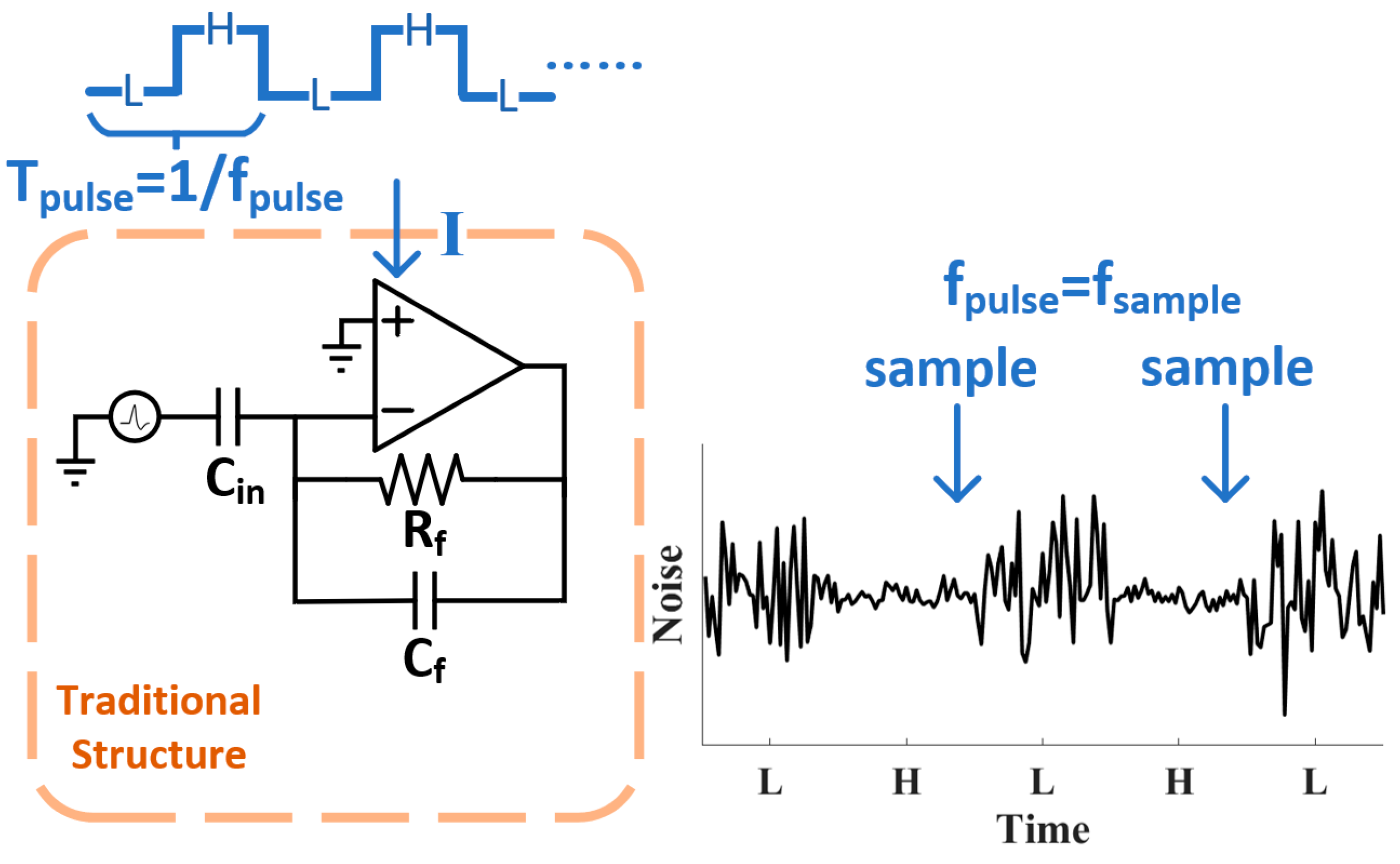
Figure 1. Neural recording amplifier and dynamic current pulsing technique. “H” represents the high current state and “L” represents the low current state.
Jlpea 15 00067 g001
Figure 2. Schematics of the neural recording amplifier. The dimensions of critical transistors are shown in the table. (a) Structure of the neural recording amplifier, incorporating the dynamic current pulsing technique. (b) The implementation of the 2-stage operational amplifier with fast settling.
Jlpea 15 00067 g002
Figure 3. Die micrograph of the fabricated three-channel neural-recording chip. Each channel has the schematic, as shown in Figure 2a.
Jlpea 15 00067 g003
Figure 4. Noise performance referred to the input of the neural recording amplifier in the LCS and HCS when using a NI DAQ 6221 to acquire the data with a sampling rate of 250 ksps.
Jlpea 15 00067 g004
Figure 5. Time domain output data when using a NI DAQ 6221 to acquire the data with a sampling rate of 250 ksps in the dynamic pulsing condition. The input voltage is 2 mVPP at 2.1 kHz. The pulsing frequency is 50 kHz with 60% time spent in the LCS. The output is shifting between the LCS and HCS with fast settling.
Jlpea 15 00067 g005
Figure 6. The input–output transfer function in the pulsing condition, LCS and HCS.
Jlpea 15 00067 g006
Figure 7. Noise performance when applying a 1st-order LPF and different pulsing duty cycles. (a,b) The pulsing frequency and the sampling frequency is at 25 kHz. (c,d) The pulsing frequency and the sampling frequency is at 50 kHz.
Jlpea 15 00067 g007
Figure 8. (a) The sample-and-hold structure. (b) Two-stage LPF: 2nd order LC filter + SH filter. (c) The timing requirements of the sampling clock and tail current controlling clock for the amplifier in Figure 2a.
Jlpea 15 00067 g008
Figure 9. (a) The transfer function of the SH structure. (b) The transfer function of the two-stage LPF.
Jlpea 15 00067 g009
Figure 10. Noise performance when applying the two-stage LPF. (a) Fourth-order digital + SH. (b) Second-order LC + SH.
Jlpea 15 00067 g010
Figure 11. Input-referred noise performance when applying a fourth-order digital filter + SH in the case of the lowest NEF of 1.55, compared to HCS and LCS. The low-frequency noise in the pulsing condition is very close to the HCS noise but the high-frequency noise is slightly larger, because of the limited settling rate. The estimated noise with the same power as the 60% LCS pulsing condition but with a constant tail current is shown with the purple line.
Jlpea 15 00067 g011
Figure 12. NEF performance comparison to state-of-the-art (publication/published year, NEF, estimated analog front-end area in mm2), with the trend line in dash. Red dots represent this work.
Jlpea 15 00067 g012
Disclaimer/Publisher’s Note: The statements, opinions and data contained in all publications are solely those of the individual author(s) and contributor(s) and not of MDPI and/or the editor(s). MDPI and/or the editor(s) disclaim responsibility for any injury to people or property resulting from any ideas, methods, instructions or products referred to in the content.