1. Introduction
With the rapid development of information technology and micro–nano photonics, low-power and high-efficiency photonic devices have become essential for modern optical communication, integrated photonic circuits, and quantum information processing [
1,
2]. Particularly in on-chip photonic systems, achieving effective power reduction while maintaining device miniaturization is a key technical challenge for realizing high-speed, low-loss information processing.
Photonic crystals (PCs), as artificially periodic dielectric structures, can control the propagation of light through the formation of photonic bandgaps, enabling light localization, waveguide transmission, and slow-light effects at subwavelength scales [
3]. These features make PCs promising candidates for constructing compact, low-power photonic devices. However, traditional photonic crystals still face challenges in achieving strong local field enhancement and efficient energy coupling, especially in further reducing threshold power and improving light utilization efficiency [
4].
To address these limitations, epsilon-near-zero (ENZ) materials—characterized by a dielectric permittivity approaching zero at specific frequencies—have attracted growing attention due to their unique electromagnetic properties [
5,
6,
7]. In the ENZ regime, electromagnetic waves exhibit extremely long wavelengths and nearly uniform phase distribution, enabling optical tunneling, field concentration, and enhanced nonlinear effects [
8,
9]. These phenomena make ENZ materials promising for pushing beyond the design constraints of traditional PCs, especially in achieving subwavelength energy transport and extreme light–matter interaction.
While ENZ materials have been previously integrated into photonic devices to leverage their extraordinary properties [
10], this study presents a distinct and previously underexplored hybrid structure: a two-dimensional photonic crystal composed of metallic cylinders embedded within an ENZ background medium. Using a rigorous electromagnetic analysis based on Fourier series expansion and modal decomposition, we reveal that the cutoff frequency of this ENZ-metal photonic crystal is invariant with respect to the volume fraction of the metal cylinders—a behavior not reported in conventional dielectric or metal–dielectric photonic crystals.
Although this study models an idealized two-dimensional structure composed of infinitely long metal cylinders embedded in an ENZ background, recent research has demonstrated the experimental viability of fabricating similar ENZ-based photonic crystal systems. ENZ behavior has been realized using metal–dielectric multilayers, such as Ag/SiO
2 and ITO/SiO
2, achieving near-zero permittivity in the optical to mid-infrared range. Techniques such as electron-beam evaporation, sputtering, and atomic layer deposition allow for precise tuning of the effective permittivity and have been widely used to fabricate hyperbolic and ENZ metamaterials [
11,
12,
13,
14]. Nonetheless, practical limitations remain. ENZ media often suffer from non-negligible optical losses near the plasma frequency, which can affect device performance. Additionally, finite-size effects, material imperfections, and fabrication-induced disorder may deviate from the idealized behavior predicted in this work. Furthermore, the transition from a 2D model to realistic 3D structures introduces edge effects and vertical confinement challenges. Despite these, progress in loss-compensated ENZ systems [
15] and non-Hermitian photonics design offers promising routes to mitigate such limitations.
This finding marks a notable departure from previous ENZ research, which has primarily emphasized field enhancement, narrowband resonances, or nonlinearities in uniform or layered media. In contrast, our results demonstrate a volume-insensitive cutoff behavior, tied to the ENZ environment’s effective permittivity and its influence on the photonic band structure. Furthermore, we uncover backward leaky mode characteristics—manifested as attenuation constant sign reversals under periodic boundary conditions—which relate to non-Hermitian photonics in ENZ regimes, an area that remains insufficiently explored.
Taken together, these insights establish a new paradigm for ENZ-integrated photonic crystal design, enabling the development of broadband, low-loss, and geometry-robust waveguide structures. Our results not only expand the theoretical understanding of ENZ-PC interactions but also provide a pathway for next-generation photonic integration platforms.
2. Theoretical Model and Derivation
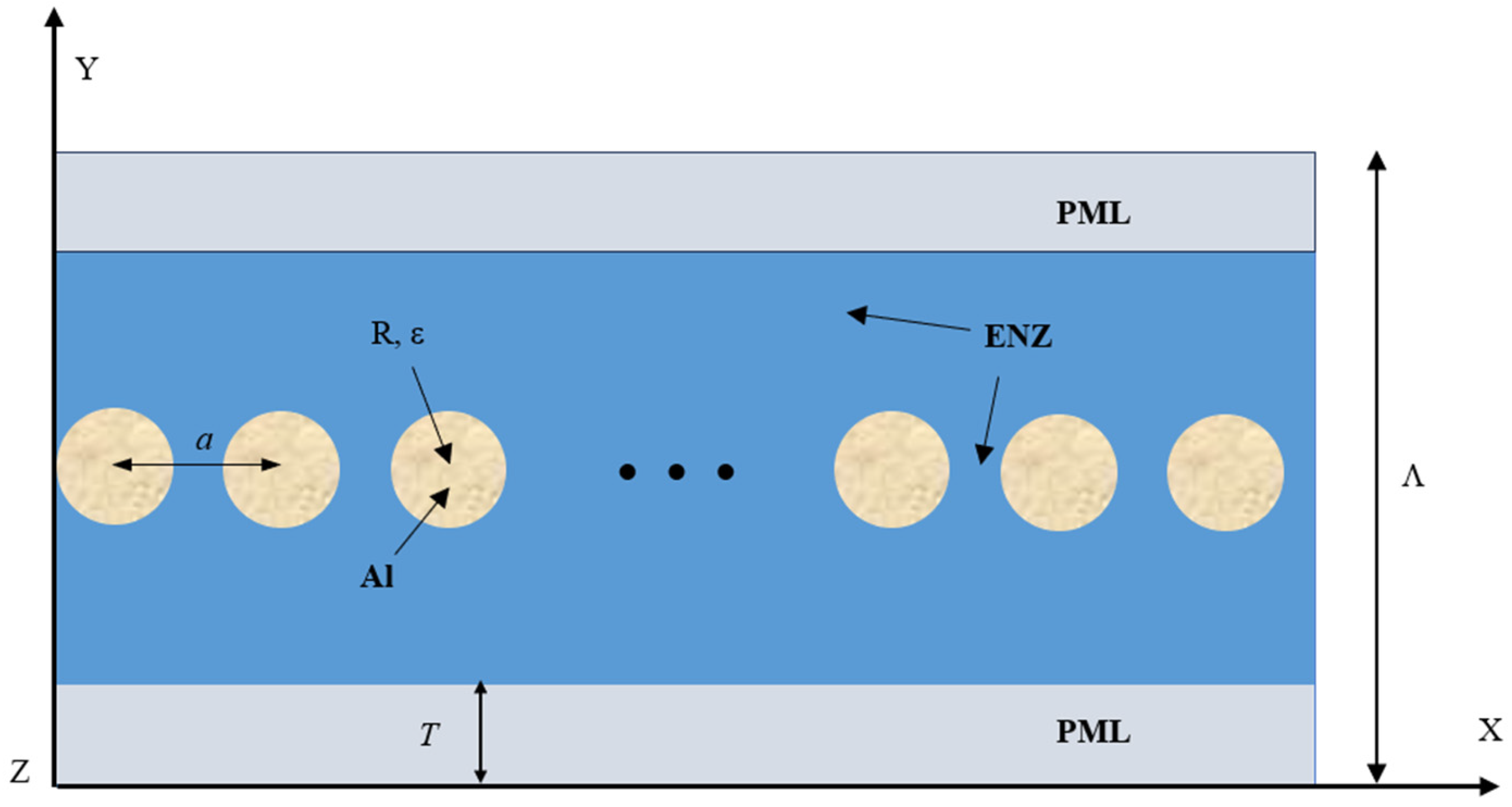
Figure 1 is a side view of the periodic structure of a two-dimensional photonic crystal, which is composed of many metal cylinders and the metal is aluminum (Al). Each scatterer is infinitely long in the Z direction and parallel to each other and the structure is periodic along the X-axis.
R is the radius of the metal cylinder,
a is the lattice constant of the photonic crystal, and
h = 550 nm is the periodicity along the X-axis, which equals
a in this model. The lattice is square. To reduce the propagation loss and better use the Fourier series expansion method, this study introduces a perfectly matched layer (PML) with a thickness of T. This layer’s wave impedance perfectly matches that of the medium next to it; the incident wave does not reflect when it touches the PML layer and enters the PML in a state of reflection loss.
The gaps between the cylinders are filled with ENZ material with
. As illustrated in
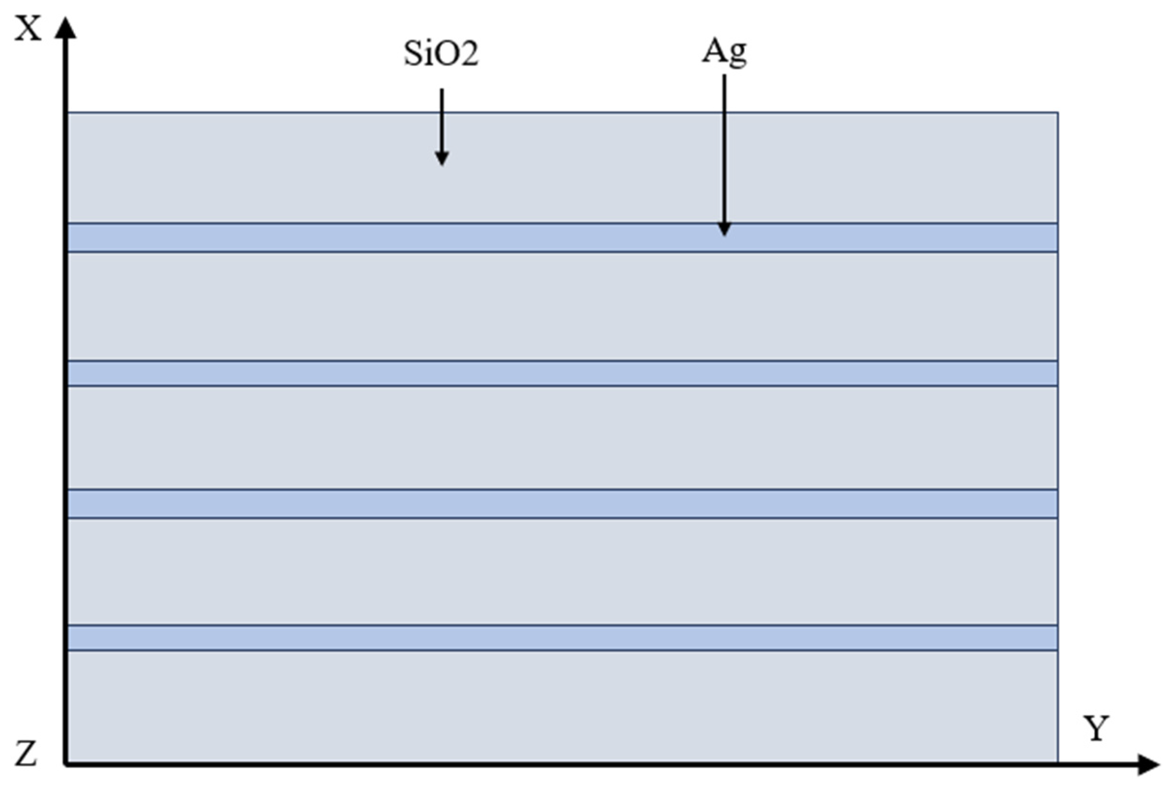
Figure 1, the ENZ medium layer is specifically composed of a silver (Ag)-silicon dioxide (SiO
2) composite (
Figure 2) [
16,
17,
18].
Dielectric materials have a positive permittivity at optical frequencies, whereas metals have a negative permittivity. Therefore, the combined value of these two types of materials may be close to zero on a weighted average basis [
19]. The resulting anisotropic effective permittivity is equal to:
where
and
represent the thickness and permittivity of the metal layer, respectively, and the components are parallel to and perpendicular to the plane. Additionally,
and
stand for the dielectric layer’s thickness and permittivity, respectively.
This study notes that the dielectric constant
and the refractive index
are all plural. Therefore, even if the real part of
disappears, the imaginary part usually remains non-zero. Both the real and imaginary components of
n do not vanish completely. The effect of the virtual dielectric constant’s effect on the refractive index may be large in many materials. Supposing no magnetic response, the subsequent formula for a zero dielectric constant wavelength decides the real part of the refractive index:
Metals, as dispersive media, require the use of dispersion models in numerical simulations to obtain their corresponding parameters. For instance, parameters such as the plasma frequency and the electron collision frequency directly affect the simulation results of dispersion-based numerical methods. In this work, both metals and degenerately doped semiconductors exhibit dielectric dispersion curves described by the Drude model [
20], which characterizes the behavior of free electrons:
where
is the dielectric constant at high frequencies,
is the electronic damping term, and
is the plasma frequency, given by:
where
represents the free electron volume density and
symbolizes the electron effective mass.
The Fourier series expansion method is employed [
20,
21,
22,
23,
24]. For the TE wave, Maxwell’s equations are as follows:
where
,
is the stretching coordinate variable [
25]; the conductivity function is
. The electric and magnetic fields are roughly represented as shortened Fourier series throughout the imaginary period of the propagating field, as follows:
where
. By substituting Equations (8)–(10) into the governing Equations (5)–(7), then multiplying the resulting expressions by
and integrating over the periodic interval 0 ≤ y ≤ Λ, we derive a system of coupled linear equations governing the Fourier expansion coefficients
and
as follows:
with
where
is Kronecker
; the superscript
denotes the vector’s transpose; and
is the permittivity along the y-axis in the interval
. The modal propagation characteristics of the waveguide structure are fully characterized by the eigensystem solution of matrix
, where the eigenvalues
and corresponding eigenvectors
determine both the complex propagation constants and the spatial field distributions for all supported guided and radiation modes. The general solution to Equations (11) and (12) can be expressed in terms of these eigenstates as:
In the formula, represents the n-order modal amplitude of forward wave and reverse wave.
When studying the transmission of optical waveguides, the eigenmode field analysis method based on Fourier series expansion is highly suitable. A side view along the two discontinuous surfaces of the waveguide is shown in
Figure 3:
Where waveguides
and
are connected at
, and
and
are connected at
. On a single waveguide interface, this study still assumes that the upper and lower layers are PML layers, and the entire period length is
. At each step discontinuity interface, the boundary conditions for
,
are enforced by equating their Fourier coefficients
and
across the interface. At the interface
, the scattering matrix
takes on the following relationship:
The definition of the scattering matrix
at
is the same as in Equation (27). Furthermore, the mode propagation at distance
must be considered in this study, as follows:
Equation (23) defines
. Equations (29)–(35) express the recurring relationship of the waveguide scattering matrix at each discontinuity point. If there exist
N step discontinuities along the waveguide at
, a recursive procedure generalizes
of the system as follows:
We investigate the calculation of the generalized scattering matrix in the
direction in each cycle
using the connection in Equation (36). The transition matrix
is obtained based on the calculation results:
As a result, Equation (38) determines the propagation constant
of the
mode:
where
is the
eigenvalue of the transfer matrix
. The propagation constant
of the
guided mode can be calculated using Floquet’s theorem via the following relation:
3. Calculation Results and Verification
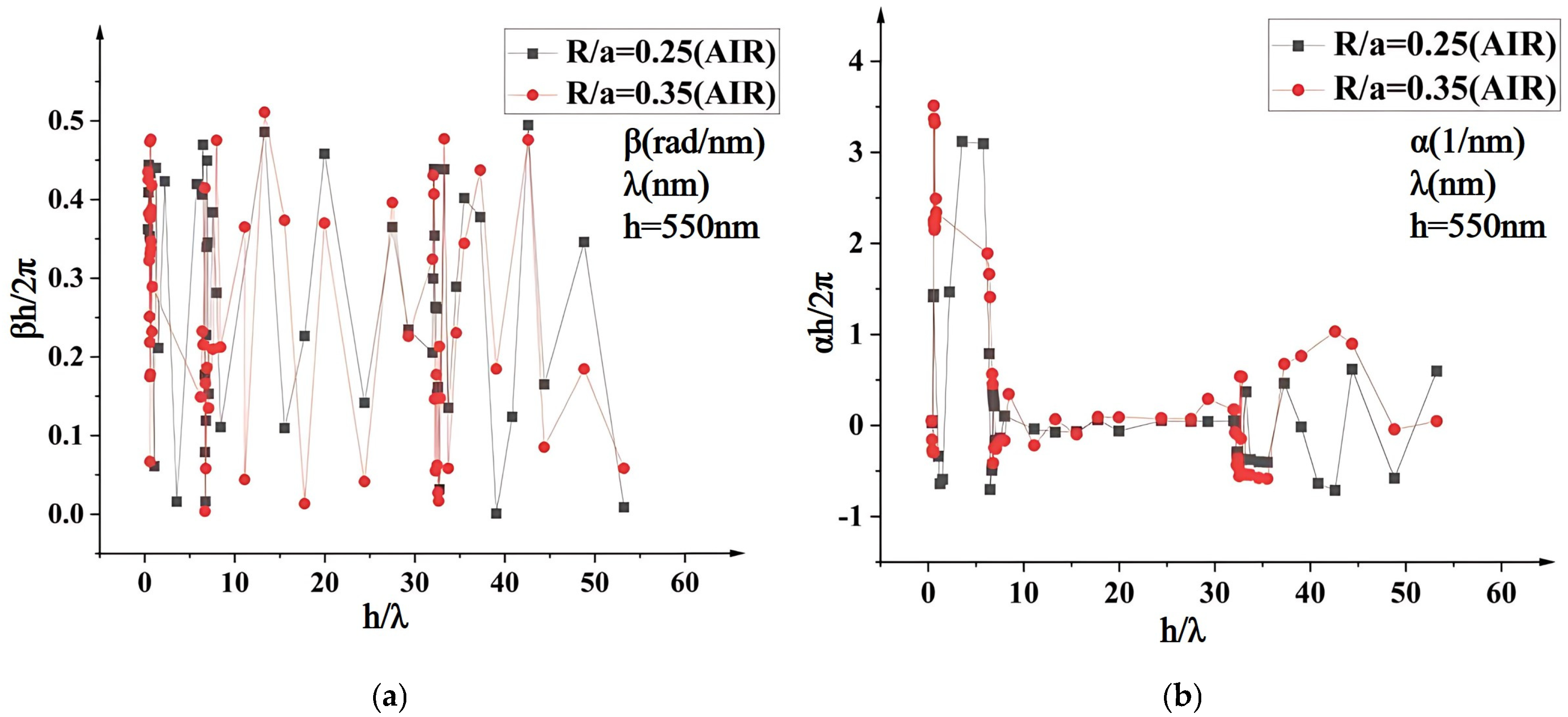
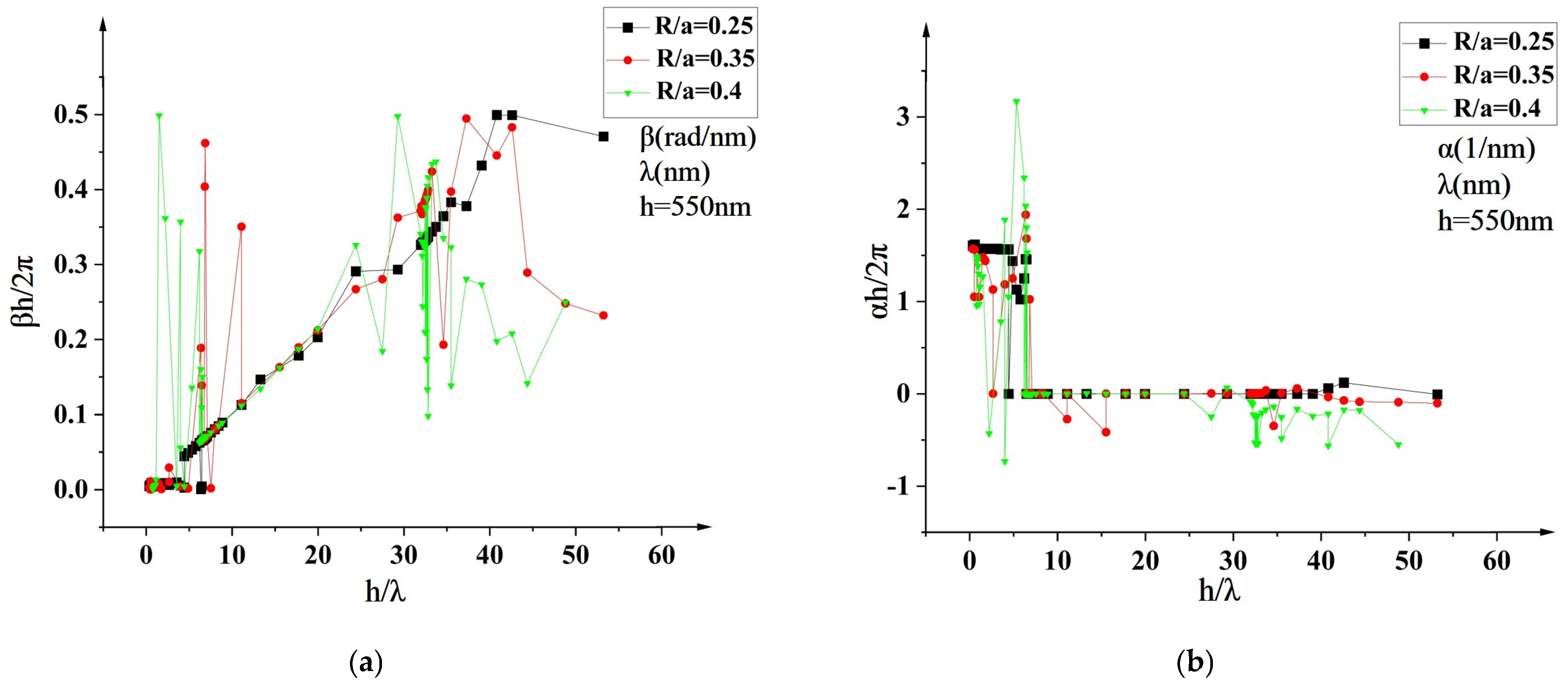
The transmission characteristics of a photonic crystal composed of air and aluminum (Al) cylinders were first investigated. In this study, all frequency values are expressed in normalized units, defined as
h/λ, and λ is the free-space wavelength. This normalization reflects the relative relationship between various length parameters and the wavelength within the model, and is used in this study to characterize the optical properties of materials. The phase constant β and attenuation constant α are written in the normalized form because this makes the values unitless and scalable and comparable across different structures, particularly those with different characteristic sizes
h or operating wavelengths λ. By writing β and α in the form βh/2π, we are comparing the propagation characteristics relative to the wavelength and to the characteristic size
h of the structure. βh/2π quantifies the number of effective wavelengths accommodated within the distance
h along the direction of propagation and the normalized form αh/2π indicates the fractional attenuation per unit of spatial period. The simulated wavelength range in
Figure 4 and
Figure 5 has been defined from 10 nm to infinity (corresponding to the condition where
h/λ = 0). It was found that as the volume fraction increases, the range of attenuation bands at both ends expands, as shown in
Figure 4.
Figure 4a,b show that when
R/
a = 0.25, the first attenuation normalized frequency range is 0.07 <
h/λ < 8.0, and the second attenuation range is 32.3 <
h/λ < 53.2. When
R/
a = 0.35, the first attenuation range is 0.07 <
h/λ < 11.1, and the second attenuation range is 26.3 <
h/λ < 53.2. As demonstrated in
Figure 4b, the condition αh/2π < 0 fundamentally characterizes the unique electromagnetic behavior of backward-propagating leaky modes under periodic boundary conditions. In such non-Hermitian periodic systems, when the structure satisfies the negative group velocity criterion (i.e., group velocity opposing phase velocity direction), the actual energy propagation direction becomes decoupled from the phase progression, inducing sign inversion of the phase constant (βh/2π → −βh/2π). By redefining the coordinate system with reference to energy flow direction (via transformation z→ −z), βh/2π regains positive values, while αh/π naturally exhibits negativity due to coordinate orientation adjustment. This sign convention discrepancy originates from reference frame optimization in eigenmode analysis, independent of wave energy dissipation/gain mechanisms. This theoretical framework has been rigorously demonstrated in [
26,
27], where analogous sign inversion of attenuation constants under periodic boundaries was experimentally observed.
Figure 5 depicts the research results of the phase constant and decay constant of metal photonic crystals consisting of near-zero materials and metal nano-cylinders.
The results of this work, however, reveal that the cutoff normalized frequency of photonic crystals consisting of metal cylinders and a near-material-free background is volume fraction independent. The phase constant (a) and attenuation constant (b) diagrams in
Figure 5 show that when
R/
a grows, the cutoff normalized frequency point remains constant at roughly
h/λ = 6.47. Light of extremely long wavelengths
, where
is a wavelength in free space, leads to this interesting phenomenon in epsilon-near-zero matter [
28,
29]. Because the light is entirely reflected from metals below the plasma frequency, the cutoff frequency of metal–dielectric photonic crystals is similar to that of the plasma frequency of metals. As a result, this cutoff frequency is known as the metal medium’s effective plasma frequency. The metal cylinder’s normalized plasma frequency is
—the effective plasma frequency does not change; even if
R grows, it remains constant at the normalized plasma frequency. The effective dielectric constant of the metal dielectric photonic crystal in the larger wavelength range (
), or in the TE mode with a very tiny volume fraction, is
, where
is the dielectric constant of the background medium and
is the volume fraction of the metal cylinder [
30]. When the medium background is air
,
. Because of
,
where
is the effective plasma frequency [
31]. When
, the effective plasma frequency corresponds to the metal dielectric photonic crystal’s cut-off frequency, because when
, the light dissemination is prohibited. When this study replaces the background medium with a near-zero material (ENZ), the effective permittivity of this study is
, where
and
. Consequently, the effective plasma frequency is independent of volume fraction size and equal to the plasma frequency of the metal cylinder.
In addition, this study also found that with the increase of the volume fraction, the area of the scattering unit increases, the phenomenon of light reflection and refraction intensifies, more collisions occur between the forward wave and the reverse wave, and the formed coupling wave can be an amplified wave. It may be a damped wave, which cannot propagate normally. Therefore, the range of the cutoff frequency band, at high frequencies, becomes wider. Utilizing this characteristic, this work filters out the electromagnetic waves of specific wavelength bands from the intermediate frequency band by increasing or decreasing the ratio of R/a. By reducing R/a, we find it is possible to manufacture waveguide devices with lower loss and a wider wavelength range for the resulting waveguide.
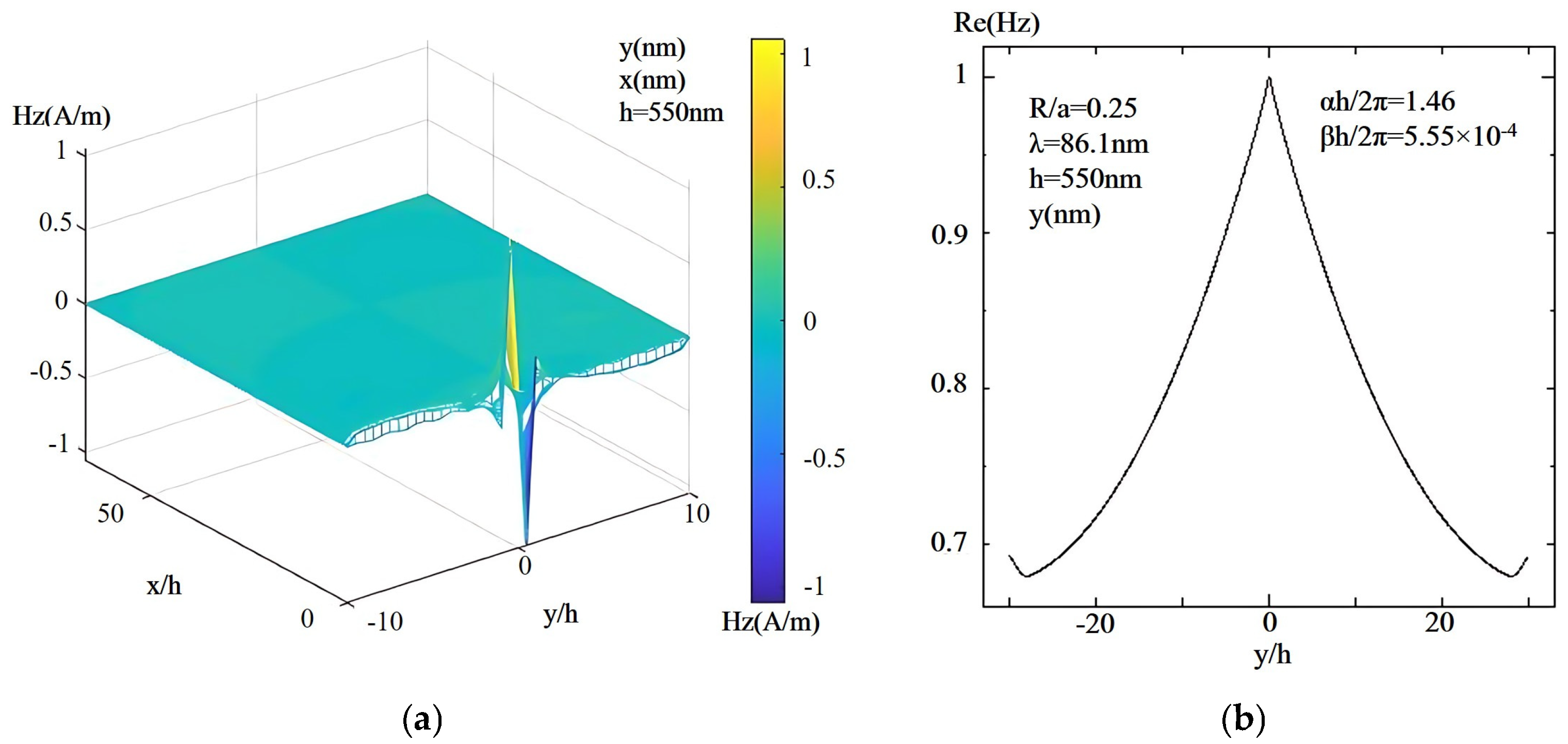
Next, we analyze the wave guiding ability and propagation distribution characteristics. This study uses a photonic crystal made of 40 metal cylinders and near-zero materials as the research object to validate the veracity of the preceding results. The capability of the resulting planar waveguide induced by the finite array at a specific wavelength is shown. To avoid repeated descriptions, the finite array propagation characteristics at
R/
a = 0.25 were studied and calculated to verify the above results. The following research indicates that in the range of 0.07 <
h/λ < 6.47, the state of light is in the cut-off state.
Figure 6 depicts the field mode distribution diagram and propagation distribution diagram with
h/λ = 6.39. The propagation distribution diagram shows the real part of the magnetic field component Hz which is normalized to the maximum value as a function of the normalized transverse coordinate y/
h, where
h is a characteristic length scale of the structure and the plot is for a specific wavelength λ = 86.1 nm. The near-field propagation distribution diagram illustrated in
Figure 6 in this study reveals that light propagation is cut off.
The propagation status is in the 6.47 <
h/λ < 39 range.
Figure 7 depicts the field mode distribution diagram and propagation distribution diagram when
h/λ = 24.44. The near-field propagation distribution diagram in
Figure 7 shows that light is in a propagating state.
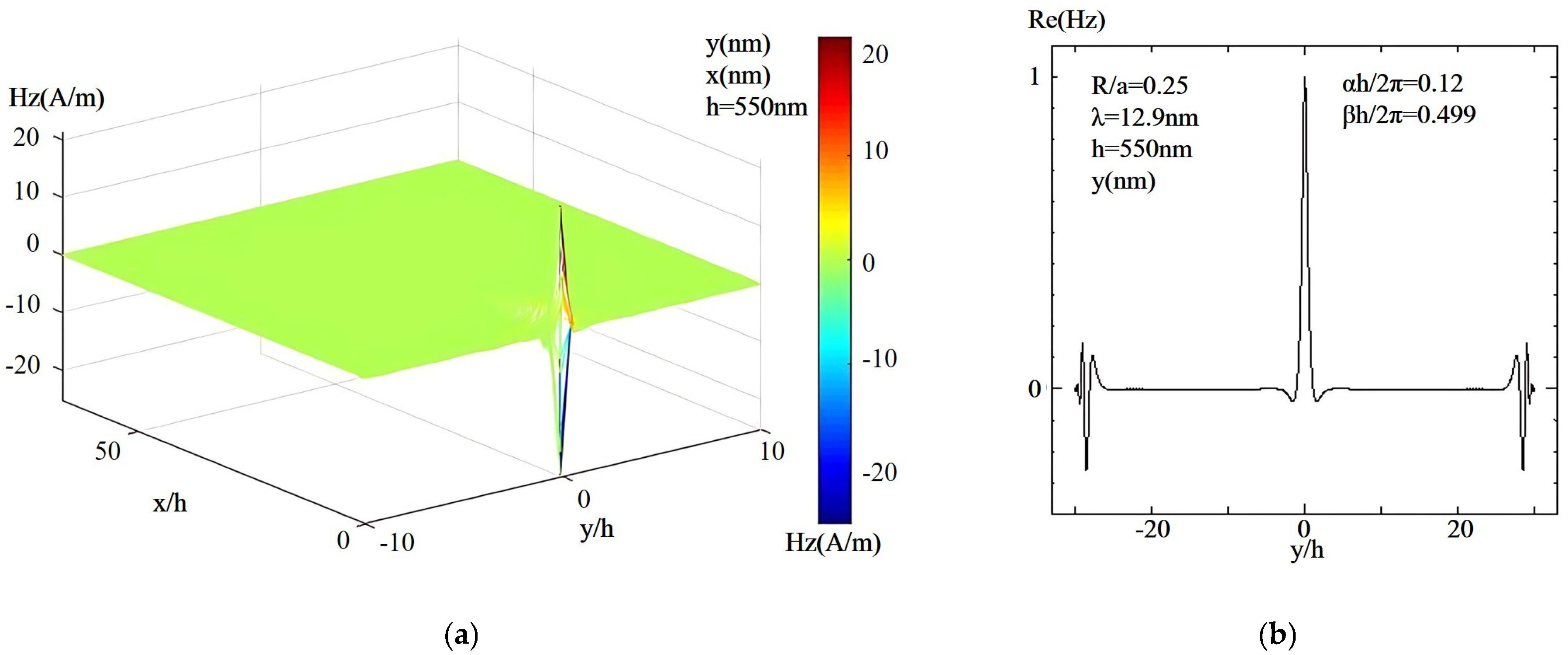
When
h/λ is greater than 39, the state of light appears (again) in the cutoff normalized frequency segment. The field mode distribution diagram and propagation distribution diagram at
h/λ = 42.59 are shown in
Figure 8. The near-field propagation distribution diagram in
Figure 8 shows the light is in a cut-off propagation state.
4. Conclusions
This study discusses the propagation characteristics and field distribution properties of photonic crystals composed of near-zero materials and metal cylinders. There is currently a lack of comprehensive research covering this aspect in the academic community.
Our findings reveal a key phenomenon: the cutoff frequency of photonic crystals composed of metal cylinders embedded in an ENZ background remains invariant with respect to the volume fraction. Within the measured frequency range, the photonic crystal exhibits three distinct frequency regions—cutoff, propagation, and cutoff again. By controlling the R/a parameter, we demonstrate the ability to tailor the range of the propagation region, enabling selective filtering of specific wavelength bands. Notably, reducing R/a allows the fabrication of waveguides with lower losses and a broader operational bandwidth, making this approach promising for photonic integration and on-chip applications.
In the context of recent work on ENZ-based photonic crystals and metamaterials, this study offers a novel contribution. While previous research has focused on ENZ materials for enhancing light–matter interactions, field localization, and nonlinear effects, our work extends these findings by showing that the cutoff frequency becomes insensitive to geometric parameters in ENZ-metal photonic crystal systems. This behavior stands in contrast to conventional metal–dielectric structures where geometry heavily dictates photonic band structures. Moreover, we observe attenuation constant sign inversions associated with backward leaky modes in the ENZ regime, linking this phenomenon to the broader field of non-Hermitian photonics—a connection that remains underexplored. Finally, this study proposes a robust design strategy for developing broadband, low-loss waveguide devices that do not require fine structural tuning, an advance over previously reported narrowband ENZ systems. While this simplification enables analytical clarity and focuses on in-plane propagation physics, it does not capture finite-size effects in the third dimension. Therefore, future work may include three-dimensional full-wave simulations or experimental validations to assess the impact of finite z-directional confinement and to further confirm the generalizability of our results.


