Abstract
Bipolar power supply can effectively reduce line losses and optimize power transmission. This paper proposes a low-power bipolar DC–DC converter with voltage self-balancing, which not only achieves bipolar output but also automatically balances the inter-pole voltage under load imbalance conditions without requiring additional voltage balancing control. This paper first elaborates on the derivation process of the proposed converter, then analyzes its working principles and performance characteristics. A 400 W experimental prototype is built to validate the correctness of the theoretical analysis and the voltage self-balancing capability. Finally, loss analysis and conclusions are presented.
1. Introduction
Under the intensifying pressures of both environmental protection and energy shortages, the development of clean renewable energy has become an inevitable necessity for the global energy transition [1,2,3,4,5,6,7,8]. In this context, bipolar DC microgrids demonstrate superior advantages due to their three-wire bipolar power supply configuration, which effectively reduces line losses, optimizes power transmission, and offers enhanced compatibility with renewable energy integration as well as improved power supply reliability. However, inter-polar voltage deviations tend to occur in such systems as a result of the unbalanced distribution of positive/negative pole sources and loads. Consequently, it is often necessary to add bipolar DC–DC converters as voltage balancers to maintain the balance between bipolar voltages [9,10,11,12,13,14].
In existing research, bipolar DC–DC converters are primarily categorized into isolated type and non-isolated type. A series of isolated bipolar DC–DC converters have been proposed in [15,16,17,18,19] to effectively achieve balanced bipolar output voltages. However, these converters have limitations such as large size, complex control mechanisms, and higher costs. Non-isolated converters offer advantages such as compact size, low cost, and simple control. They are often preferred for low-power applications like photovoltaic power generation. Various non-isolation bipolar DC–DC converters are developed in [20,21,22,23,24,25,26,27,28,29,30,31]. In [20,21,22,23], bidirectional Buck/Boost structures are utilized to construct bipolar converters functioning as voltage balancers. These converters regulate the inter-terminal power flow in bipolar DC microgrids, thus maintaining a balanced bipolar voltage. To reduce device stress, three-level converters are employed in [24,25,26,27] to construct bipolar DC–DC converters. However, the demands on the switching component increase, complicating the system control and driving methods. According to [28,29], traditional Boost converters are integrated with Buck/Boost or Zeta converters to form hybrid topologies. However, due to the inconsistent voltage gains among the basic converter branches, distinct control parameters are required to ensure equal output voltages. Coupled inductors and voltage multiplier (VM) circuits are integrated into bipolar DC–DC converters in [30,31] to enhance voltage gain, utilizing magnetic coupling effects to boost output voltages. Furthermore, the topologies lack scalability and exhibit insufficient voltage gain, failing to meet the significant voltage conversion demands required for interfacing new energy generation units with bus systems in modern renewable energy applications.
In this paper, a novel non-isolated bipolar self-voltage-balancing DC–DC converter is proposed, which can automatically balance the inter-polar voltages under unbalanced bipolar output loads without additional balance control mechanisms. The proposed converter features scalability in its structure, while the expansion units contain no active switches. By adjusting the number of expansion units, the voltage gain and device stress can be regulated, which further enhances topological flexibility. Furthermore, the circuit only incorporates a single active switch, and the control method is simple, which is consistent with that of the traditional Boost converter. The remaining sections are organized as follows: Section 2 derives the converter’s configuration and provides a detailed analysis of its operating modes. Section 3 analyzes the voltage gain characteristics and voltage/current stress properties of the proposed topology, which are further compared with several existing bipolar converters. In Section 4, a 400 W experimental prototype is constructed to validate the theoretical analysis and demonstrate the characteristics of the proposed converter. Finally, relevant conclusions are presented in Section 6.
2. Topology Derivation and Working Principles
The traditional Boost converter, as shown in Figure 1a, features a continuous input current and a simple structure that has been widely applied. However, its unipolar output is unsuitable for bipolar DC microgrids. To construct a bipolar configuration, this work incorporates a negative branch composed of capacitors and diodes into the traditional Boost circuit, as depicted in Figure 1b. In this bipolar topology, the positive output port is implemented by the Boost converter with a voltage of UP, and the negative output port is implemented by the negative branch with a voltage of UN. In the proposed topology, when diode D3 is turned on, the intermediate capacitor C1 is connected in parallel with the negative output port, and the voltage at the negative output port is the voltage of the intermediate capacitor C1, as shown in mode 1 of Figure 1c. When diodes D1 and D2 are turned on, the intermediate capacitor C1 is connected in parallel with the positive output port. At this time, the voltage at the positive output port is the voltage of the intermediate capacitor C1, as shown in mode 2 of Figure 1c. Therefore, through the alternating operation of the diodes, the intermediate capacitor is alternately connected in parallel with the output ports. By using the property that the capacitor voltage cannot change abruptly, the output port voltages are kept the same, so as to realize the self-balancing of the output voltage without additional control mechanisms, and the method that realizes the inter-pole voltage balance only by the topology without using the voltage balance control method is defined as voltage self-balancing. Considering that conventional Boost converters exhibit limited voltage gain and fail to meet the high gain demands in renewable energy applications, this work also extends the structure in Figure 1b by integrating expansion branches to both the positive and negative branches, as shown in Figure 1d. This enhancement effectively increases output voltage while maintaining the simple control and driving methods, since there are no active switches in the expansion modules. The expansion modules allow flexible configuration to meet specific voltage gain requirements and alleviate device stress according to engineering needs.
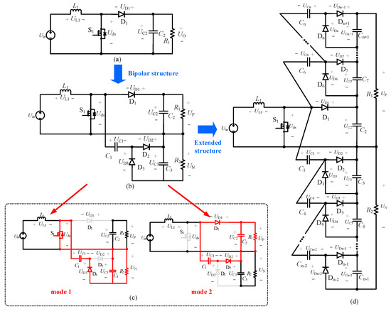
Figure 1.
Topology derivation. (a) Traditional Boost converter. (b) Proposed converter. (c) Equivalent circuits of the two working states. (d) Proposed converter with the extended unit.
The analysis of operating modes for the proposed converter is presented in this section using the bipolar converter shown in Figure 1b. The following assumptions are made:
- The converter operates under continuous conduction mode (CCM);
- All components are assumed to be ideal, and their parasitic parameters are neglected;
- Capacitors are sufficiently large to neglect voltage ripple effects.
The primary waveforms and equivalent circuit diagrams of the proposed converter within one switching cycle are illustrated in Figure 2, Figure 3 and Figure 4, respectively. The specific operating mode analysis is detailed as follows:
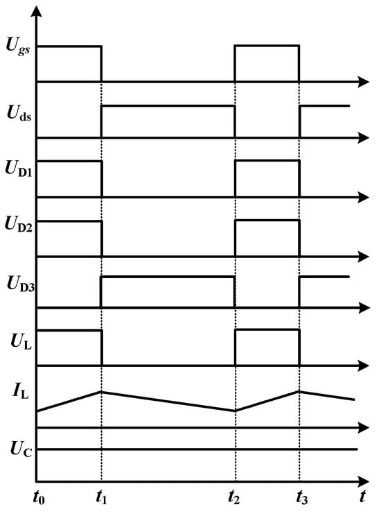
Figure 2.
The primary waveforms within one switching cycle.
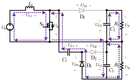
Figure 3.
Mode I: When switch S1 is conducting, diode D3 conducts, while diodes D1 and D2 are reverse-biased. The input voltage source Uin, inductor L1, and switch S1 form a closed loop. The inductor L1 is charged and its current rises linearly. Meanwhile, a path is formed by switch S1, capacitor C1, diode D3, and capacitor C3. The capacitor C1 is in parallel with the output capacitor C3 (assuming negligible voltage ripple). Under this configuration, UC1 equals UC3. Load R1 is provided by capacitor C2, while load R2 is supplied by capacitor C3.
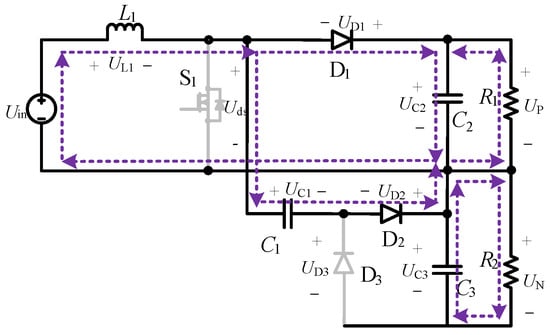
Figure 4.
Mode II: When switch S1 is turned off, diodes D1 and D2 become forward-conducting, while diode D3 is reverse-biased. The input voltage source Uin forms two discharge loops with inductor L1. The first discharge loop is formed via D1-C2 (constituted by Uin-L1-D1-C2) and the second discharge loop is formed via D2-C1 (constituted by Uin-L1-D2-C1), thereby enabling the discharging process of L1. When capacitor voltage ripples are neglected, a steady-state equilibrium is achieved where the voltages across capacitors C1 and C2 satisfy UC1 = UC2 due to the conductive path formed by D1, D2, C1, and C2.
Since the voltage across a capacitor cannot undergo abrupt changes, within one switching cycle, it holds that UC1 = UC2 = UC3. By utilizing capacitor C1 as an intermediate component, this configuration establishes a voltage-balancing loop for the output voltage, thereby maintaining the output voltage clamped to the voltage of capacitor C1 without requiring additional voltage balance control mechanisms.
3. Performance Analysis
3.1. Voltage Gain Analysis
According to the volt-second equilibrium of the inductor L1, it can be obtained that
where D is the duty cycle of switch S1, Uin is the input voltage, and UP is the positive output voltage.
According to the above equation, the positive voltage gain MP of the converter can be obtained as
In the same way, according to the volt-second equilibrium of the inductor L1 in the negative branch, we can obtain:
where D is the duty cycle of switch S1, Uin is the input voltage, and UN is the negative output voltage.
The negative voltage gain MN is as follows:
Therefore, the voltage gain of the converter is obtained:
Extending the equation to a topology with n expansion units, the expression for the voltage gain is as follows:
3.2. Voltage and Current Stress Analysis of the Device
When the switch is turned on, the diodes D1 and D2 are turned off, and the voltage stresses of the diodes D1 and D2 are determined according to
When the switch is turned off, the voltage stress of switch S1 and diode D3 is
Similarly, according to the loop in the second mode, the capacitor voltage stresses are as follows:
Extending the equation to the topology with n expansion units, the expression of the voltage stress of the device in the topology is as follows:
Ignoring the influence of the current ripple, the direct flow of current of each element is recorded as IS1, IL1, ID1, ID2, ID3, IP, and IN. According to the circuit mode analysis in the former section, the average values of the current on diodes D1, D2, and D3 are consistent with the output currents of bipolar branch as
Ignoring the loss of the converter, according to the relationship between the equality of the input and output power and the voltage gain, the input current Iin, the current stress of the inductor L1, and the switch S1 are obtained:
Extending the above current stress analysis to the topology with n expansion units, the expression of the current stress of the device in the topology is as follows:
3.3. Comparative Analysis
Compared with several non-isolated bipolar topologies listed in Table 1, the converter proposed in this paper exhibits higher flexibility and adjustable voltage gain than the converters in [12,17]. In comparison with the topologies in [17,20], the proposed converter has the advantages of fewer power devices and simpler control schemes, while device stress can be reduced through expansion unit additions. Unlike the structure proposed in [20], the proposed converter contains only one active switch with the same voltage gain characteristics for both positive and negative terminals, simplifying control and driving methods. Compared with the converter in [22], the proposed converter achieves high voltage gain, and the voltage gain can be adjusted while employing fewer magnetic components to effectively reduce size, weight, and electromagnetic interference. Most significantly, the proposed topology successfully realizes self-voltage balancing at bipolar output terminals without requiring complex voltage balancing control mechanisms, which distinguishes it from all aforementioned converters.

Table 1.
Comparison of data.
4. Experimental Validation
To validate the theoretical analysis presented above, an experimental prototype with a rated power of 400 W is constructed in this work. The parameters of the prototype are detailed in Table 2, and its configuration is illustrated in Figure 5.
Table 2.
Experimental prototype parameters.
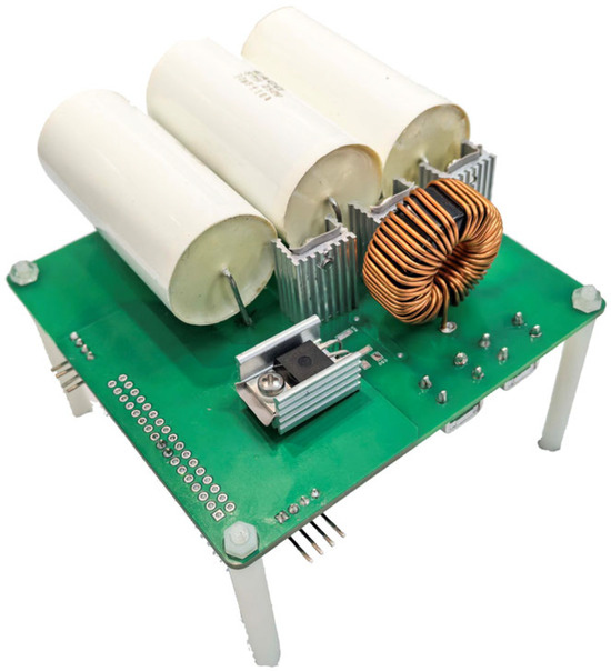
Figure 5.
Experimental prototype diagram.
4.1. The Experimental Results of the Steady-State
Under rated operating conditions, the steady-state experimental waveforms are shown in Figure 6. Figure 6a illustrates the switch voltage waveforms as well as the inductor voltage and current waveforms. Figure 6b shows the input and output voltage and current waveforms. Figure 6c presents the voltage and current waveforms of the positive and negative terminals. Figure 6d demonstrates the diode voltage waveform. Figure 6e depicts the capacitor voltage waveform. The experimental results indicate that under an input voltage of 72 V and a duty cycle of 0.35, the output voltages of both positive and negative terminals are approximately 110 V. When the output power reaches 400 W, the output currents for both terminals are approximately 3.64 A. The voltage stress across the diode during turn-off is approximately 153 V, while the capacitor voltages are around 110 V. These experimental results remain consistent with theoretical analysis.
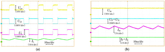
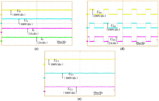
Figure 6.
Steady-state experimental waveforms. (a) Switch voltage and driver waveforms and the inductor voltage and current waveforms. (b) Input and output voltage and current waveforms. (c) Voltage and current waveforms of the positive and negative terminals outputs. (d) Diode voltage waveform. (e) Capacitor voltage waveform.
4.2. The Experimental Results of the Voltage Self-Balancing
The self-balancing of the voltage between positive and negative terminals can be quantitatively determined by calculating the Voltage Unbalance Factor (VUF%). The VUF% is defined as
The experimental waveforms are illustrated in Figure 7. As revealed by the experimental results, when the output power deviation is 200 W, the voltage deviation reaches 1.79 V with a VUF% of 0.8%. When the output power deviation reduces to 100 W, the corresponding values of voltage deviation (1.48 V) and the VUF% (0.67%) are observed. These findings effectively validate that the proposed converter exhibits outstanding self-balancing characteristics.
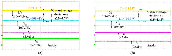
Figure 7.
Unbalanced experiment: (a) 200 W unbalanced experiment; (b) 100 W unbalanced experiment.
5. Loss and Efficiency
The losses of the converter are mainly composed of switching losses, diode losses, capacitor losses, inductor losses, and other losses. The theoretical loss analysis for each component is provided as follows:
- (1)
- Switching losses
The conduction loss of the main switching device (MOSFET) is expressed as PCON. PCON equals the product of the device’s conduction resistance (IPP200N25N, with a conduction resistance of 20 mΩ) and the square of the RMS current iS, resulting in
The switching loss of the switch device is expressed by PSW, which is
Therefore, the total loss of the main switching device is
- (2)
- Diode losses
The diode turn-on loss is expressed by PD-CON, which is equal to the forward voltage drop of the diode vF (vF = 0.55 V) multiplied by the average current through the diode. The average current of diodes D1, D2 and D3 is calculated as about 1.8 A, and the diode turn-on loss is as follows:
Since the reverse recovery current of the selected diode STTH8L06 is relatively small, its reverse recovery losses can be ignored.
- (3)
- Capacitor losses
The capacitor equivalent resistance is about 3.9 mΩ, so the capacitor loss can be calculated as
where IC1 represents the RMS value of capacitor current during operation
- (4)
- Inductor losses
- a.
- Core loss calculations:
The core model selected for the experiment is CS270125, and the core loss under experimental conditions is
- b.
- Copper loss calculation:
Checking the table, ,
- (5)
- Other losses: Approximately 0.4 W (0.1% of total power) including wire losses.
Therefore, the theoretical efficiency value of the converter is
The loss distribution of each part of the proposed converter is shown in Figure 8.
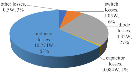
Figure 8.
Loss distribution.
The experimental and theoretical efficiency curves of the proposed converter under varying input voltages are depicted in Figure 9. The experimental prototype achieves a rated experimental efficiency and maximum experimental efficiency, both reaching 96.12% under the rated operating conditions.
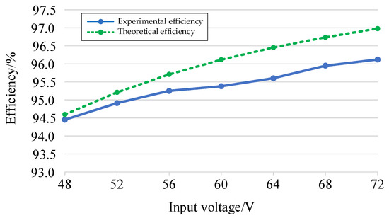
Figure 9.
Experimental and theoretical efficiency curves.
Thermal images of the converter during rated operation are presented in Figure 10. As indicated by thermal imaging analysis, the heat dissipation is mainly concentrated on the switching components. A peak temperature of 50.7 °C was recorded at the hottest location.
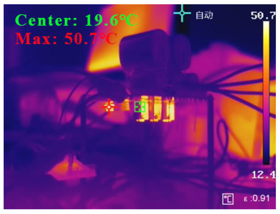
Figure 10.
Thermal imaging diagram.
6. Conclusions
This paper proposes a low-power bipolar DC–DC converter with voltage self-balancing, and through theoretical analysis and experimental verification draws the following conclusions:
- The proposed bipolar converter exhibits excellent self-balanced characteristics for the output voltages between bipolar terminals;
- The structure of the converter is simple, containing only a single active switch, and it maintains the control and driving methods of the Boost converter without any alterations;
- The proposed structure is scalable, and since there are no active components in the expansion units, it will not affect the control method of the converter.
Author Contributions
Conceptualization, Y.L. and Q.L.; methodology, Y.L.; software, Z.W.; validation, Y.L., Q.L. and Z.W.; formal analysis, Y.L.; investigation, Z.W.; resources, Y.L.; data curation, Q.L.; writing—original draft preparation, Y.L.; writing—review and editing, Y.L.; visualization, Q.L.; supervision, Z.W.; project administration, Y.L.; funding acquisition, Y.L. All authors have read and agreed to the published version of the manuscript.
Funding
This work was supported in part by the Guangxi Key Research and Development Plan Project (Grant No. AB23026037) and in part by the Key Research Plan Program of Education Department of Hubei Province (Grant No. D20231201).
Data Availability Statement
The original contributions presented in this study are included in the article. Further inquiries can be directed to the corresponding author.
Conflicts of Interest
The authors declare no conflict of interest.
References
- Hinov, N.; Grigorova, T. A Comprehensive Analysis of Losses and Efficiency in a Buck ZCS Quasi-Resonant DC/DC Converter. J. Low Power Electron. Appl. 2025, 15, 34. [Google Scholar] [CrossRef]
- Caselli, M.; Ronchi, M.; Boni, A. Power Management Circuits for Low-Power RF Energy Harvesters. J. Low Power Electron. Appl. 2020, 10, 29. [Google Scholar] [CrossRef]
- Zhu, B.; Wang, H.; Zhang, Y.; Chen, S. Buck-Based Active-Clamp Circuit for Current-Fed Isolated DC–DC Converters. IEEE Trans. Power Electron. 2022, 37, 4337–4345. [Google Scholar] [CrossRef]
- Zhu, B.; Yang, Y.; Wang, K.; Liu, J.; Vilathgamuwa, D.M. High Transformer Utilization Ratio and High Voltage Conversion Gain Flyback Converter for Photovoltaic Application. IEEE Trans. Ind. Appl. 2024, 60, 2840–2851. [Google Scholar] [CrossRef]
- Babu, V.V.; Roselyn, J.P.; Sundaravadivel, P. Coordination of SRF-PLL and Grid Forming Inverter Control in Microgrid with Solar PV and Energy Storage. J. Low Power Electron. Appl. 2024, 14, 29. [Google Scholar] [CrossRef]
- Shaukat, H.; Ali, A.; Ali, S.; Altabey, W.A.; Noori, M.; Kouritem, S.A. Applications of Sustainable Hybrid Energy Harvesting: A Review. J. Low Power Electron. Appl. 2023, 13, 62. [Google Scholar] [CrossRef]
- Ibude, F.; Otebolaku, A.; Ameh, J.E.; Ikpehai, A. Multi-Timescale Energy Consumption Management in Smart Buildings Using Hybrid Deep Artificial Neural Networks. J. Low Power Electron. Appl. 2024, 14, 54. [Google Scholar] [CrossRef]
- Udeji, U.L.; Margala, M. OptimalNN: A Neural Network Architecture to Monitor Chemical Contamination in Cancer Alley. J. Low Power Electron. Appl. 2024, 14, 33. [Google Scholar] [CrossRef]
- Yang, Y.; Zhu, B.; She, X.; Wang, K.; Liu, A. A Family of Bipolar DC–DC Converters with Interpolar Voltage Self-Balancing Based on FB-BVMs for BLVDC Microgrid. IEEE Trans. Ind. Electron. 2025, 1–10. [Google Scholar] [CrossRef]
- Yang, Y.; Zhu, B.; She, X.; Wang, K.; Liu, A. A Family of Voltage Balancers with Fault-Tolerance and Interpolar Voltage Self-Balancing Ability for Bipolar DC Power Systems. IEEE Trans. Transp. Electrif. 2025, 11, 9864–9876. [Google Scholar] [CrossRef]
- Ren, Q.; Han, Y.; Zhou, M.; Yan, C.; Yang, P.; Wang, C. Overview of Voltage Balancing Schemes in Bipolar DC Microgrids. IEEE Trans. Power Electron. 2025, 40, 3469–3489. [Google Scholar] [CrossRef]
- Pires, V.F.; Cordeiro, A.; Roncero-Clemente, C.; Rivera, S.; Dragičević, T. DC-DC Converters for Bipolar Microgrid Voltage Balancing: A Comprehensive Review of Architectures and Topologies. IEEE J. Emerg. Sel. Top. Power Electron. 2022, 11, 981–998. [Google Scholar] [CrossRef]
- Rivera, S.; Lizana, R.; Kouro, S.; Dragičević, T.; Wu, B. Bipolar DC Power Conversion: State-of-the-Art and Emerging Technologies. IEEE J. Emerg. Sel. Top. Power Electron. 2021, 9, 1192–1204. [Google Scholar] [CrossRef]
- Wang, F.; Lei, Z.; Xu, X.; Shu, X. Topology Deduction and Analysis of Voltage Balancers for DC Microgrid. IEEE J. Emerg. Sel. Top. Power Electron. 2017, 5, 672–680. [Google Scholar] [CrossRef]
- Liu, X.; Wu, X.; Chen, X.; Zhao, X. A bidirectional resonant CLLC converter combining three-level characteristic and bipolar DC structure. Int. J. Circuit Theory Appl. 2024, 52, 6151–6181. [Google Scholar] [CrossRef]
- Tian, Q.; Zhang, X.; Zhou, G.; Li, H.; Ma, H. Improved Dual Active Bridge DC–DC Converter with Symmetric Bipolar Output by Utilizing a Switched-Capacitor Circuit for Bipolar DC Distribution System. IEEE Trans. Ind. Electron. 2024, 71, 524–536. [Google Scholar] [CrossRef]
- Xiong, W.; Wang, M.; Ning, G.; Sun, Y.; Su, M. A ZVS Branch-Sharing Partial Power Converter with Bipolar Voltage Regulation Capability. IEEE Trans. Ind. Electron. 2024, 71, 1572–1582. [Google Scholar] [CrossRef]
- Ai, J.; Yang, X.; Shen, Y.; Ni, H.; Bi, K.; Fan, Q. A family of interleaved isolated three-level DC/DC converters. IET Power Electron. 2024, 17, 2861–2877. [Google Scholar] [CrossRef]
- Lin, Y.; Zhou, F.; Xu, G.; Xiong, W.; Ning, G. Bipolar Current-Fed DC–DC Converter with Automatic Voltage Balance and Full Range ZVS for Bipolar DC System. IEEE Trans. Power Electron. 2024, 39, 4248–4259. [Google Scholar] [CrossRef]
- Kakigano, H.; Miura, Y.; Ise, T. Low-Voltage Bipolar-Type DC Microgrid for Super High Quality Distribution. IEEE Trans. Power Electron. 2010, 25, 3066–3075. [Google Scholar] [CrossRef]
- Kim, H.-J.; Han, B.-M. Operation analysis of bipolar DC distribution system with new half-bridge voltage balancer. In Proceedings of the 2015 IEEE International Conference on Building Efficiency and Sustainable Technologies, Singapore, 31 August–1 September 2015; pp. 62–67. [Google Scholar]
- Ma, J.; Li, Y.; Zhu, M.; Cai, X. Parallel operation of distributed voltage balancers for bipolar DC system with improved reliability and efficiency. In Proceedings of the IECON 2017-43rd Annual Conference of the IEEE Industrial Electronics Society, Beijing, China, 29 October–1 November 2017; pp. 1387–1392. [Google Scholar]
- Liu, C.; Zhu, D.; Zhang, J.; Liu, H.; Cai, G. A Bidirectional Dual Buck-Boost Voltage Balancer with Direct Coupling Based on a Burst-Mode Control Scheme for Low-Voltage Bipolar-Type DC Microgrids. J. Power Electron. 2015, 15, 1609–1618. [Google Scholar] [CrossRef]
- Rivera, S.; Wu, B.; Kouro, S.; Yaramasu, V.; Wang, J. Electric Vehicle Charging Station Using a Neutral Point Clamped Converter with Bipolar DC Bus. IEEE Trans. Ind. Electron. 2015, 62, 1999–2009. [Google Scholar] [CrossRef]
- Zhang, X.; Gong, C.; Yao, Z. Three-level DC converter for balancing DC 800 V voltage. IEEE Trans. Power Electron. 2015, 30, 3499–3507. [Google Scholar] [CrossRef]
- Nisha, K.S.; Gaonkar, D.N.; Jayalakshmi, N.S. Operation and control of multiple electric vehicle load profiles in bipolar microgrid with photovoltaic and battery energy systems. J. Energy Storage 2023, 57, 106261. [Google Scholar]
- Fukuda, K.; Koizumi, H. Three-level buck-boost dc-dc converter with voltage-lift-type switched-inductor. In Proceedings of the IECON 2013-39th Annual Conference of the IEEE Industrial Electronics Society, Vienna, Austria, 10–13 November 2013; pp. 1368–1373. [Google Scholar]
- Chapparya, V.; Singh, S.P.; Dey, A. Novel Non-isolated Boost-Zeta Interleaved DC-DC Converter for Low Voltage Bipolar DC Micro-grid Application. In Proceedings of the 2022 IEEE International Conference on Power Electronics, Smart Grid, and Renewable Energy (PESGRE), Trivandrum, India, 2–5 January 2022; pp. 1–7. [Google Scholar]
- Guo, Y.; Sun, H. A Bipolar Output Active-Switched-Inductor Converter for Bipolar DC Microgrid. Int. J. Photoenergy 2022, 2022, 7252163. [Google Scholar] [CrossRef]
- Hasanpour, S.; Nouri, T. New Coupled-Inductor High-Gain DC/DC Converter with Bipolar Outputs. IEEE Trans. Ind. Electron. 2024, 71, 2601–2613. [Google Scholar] [CrossRef]
- Hasanpour, S.; Siwakoti, Y.P.; Blaabjerg, F. A new soft-switching high gain DC/DC converter with bipolar outputs. IET Power Electron. 2024, 17, 144–156. [Google Scholar] [CrossRef]
Disclaimer/Publisher’s Note: The statements, opinions and data contained in all publications are solely those of the individual author(s) and contributor(s) and not of MDPI and/or the editor(s). MDPI and/or the editor(s) disclaim responsibility for any injury to people or property resulting from any ideas, methods, instructions or products referred to in the content. |
© 2025 by the authors. Licensee MDPI, Basel, Switzerland. This article is an open access article distributed under the terms and conditions of the Creative Commons Attribution (CC BY) license (https://creativecommons.org/licenses/by/4.0/).