Abstract
This article introduces a novel digital-to-analog converter (DAC), which addresses a few weaknesses that a traditional capacitive DAC (CDAC) has, such as matching and parasitic capacitance-induced code dependency and a challenging bridge capacitor design. Our novel idea is a hybrid DAC of a CDAC and a current-steering DAC (CSDAC) and is named the CSCDAC. In this paper, a 12-bit CSCDAC is designed, and the post-layout simulation is provided. The Nyquist 12-bit CSCDAC exhibits a spurious free dynamic range (SFDR) of 67.62 dB under an operating frequency of 2 GS/s, with an expected average power of 54 mW. The 12-bit CSCDAC occupies a 0.154 mm2 die area, whereas the core area is 0.044 mm2.
1. Introduction
The capacitive digital-to-analog converter (CDAC) in Figure 1a is a standard digital-to-analog converter (DAC) topology well known for its low power consumption and low voltage compatibility. It is essential in a bigger system, such as a successive approximation register (SAR) analog-to-digital converter (ADC) and a radio transceiver. A binary-weighted CDAC contains capacitors and switches that double for every additional bit resolution. To reduce the die area’s cost, split-capacitor architecture was introduced [1]. Figure 1b shows a CDAC utilizing a split capacitor to reduce the die area by resetting the required unit capacitor () in each segmentation. Despite the die area’s advantage, the split capacitor is preferred less often than the conventional binary-weighted CSDAC due to the output code’s dependency induced by parasitic capacitance [2].
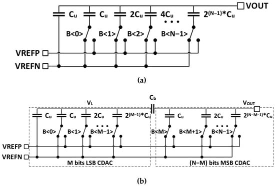
Figure 1.
Conventional DAC schematics: (a) binary-weighted CDAC; (b) split CDAC.
The work in [2] reports that the linearity of a split CDAC is limited by capacitor matching and the parasitic capacitance appearing at the least significant bit (LSB) section of the split CDAC. A split CDAC requires a bridge capacitor, where the value is challenging to realize in a regular layout [3].
This paper introduces a novel approach that addresses the above-mentioned challenges of a conventional CDAC. The proposed DAC can operate under 2 GS/s sampling frequency and support 12-bit resolution. The proposed DAC architecture has the potential to operate at a higher sampling and signal frequency while offering a higher bit resolution. Those properties are suitable for applications like envelope-tracking DACs (ETDACs) and RFDACs in cellular transmitter systems [4,5].
The organization of this paper is given as follows. Section 2 illustrates the architecture and the working principle of the proposed DAC. Section 2 also analyses its specification and compares it with the conventional CDAC. Section 3 shows the implementation of the DAC with 12-bit resolution, while Section 4 shows the simulated results and discussion. Section 5 concludes this article.
2. Design and Analysis of a CSCDAC
2.1. CSCDAC Architecture
The proposed CSCDAC combines the merits of the low-area CSDAC and the low-power CDAC to form a hybrid structure. In this CSCDAC structure, the CDAC acts as the most significant bits (MSB) sub-DAC, while the CSDAC, separated by a bridge capacitor (), forms the LSB sub-DAC. The structure is similar to a split CDAC but with the LSB CDAC replaced by a CSDAC. Due to the fully differential nature of the CSDAC, only one CSDAC is required to construct a differential CSDAC. Figure 2 illustrates a 12-bit CSCDAC with an 8-4-bit CDAC to CSDAC segmentation. The justification for using this segmentation ratio is provided in the following section.
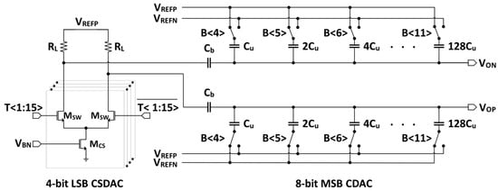
Figure 2.
A 12-bit CSCDAC with 8-4 segmentation.
2.2. CSCDAC Operating Principle
In this section, a single-ended CSCDAC shown in Figure 3 is analyzed instead of the fully differential version. One plate of the bridge capacitor, is connected to the CDAC charge summing node, which is also the CSCDAC output, whereas another plate of the bridge capacitor is connected to the CSDAC output.
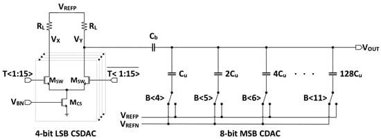
Figure 3.
A 12-bit single-ended CSCDAC.
When the digital word is sent to the CSDAC, the CSDAC steers the current from the current source to the corresponding output terminal. An output voltage is then built up by the current proportional-to-digital input and the termination resistance, . The voltage at the CDAC output due to the LSB sub-DAC, , is, therefore, a capacitive divided CSDAC output.
where is the total capacitance of the MSB CDAC, and is the output voltage of the CSDAC.
Each CDAC element consists of a capacitor and a pair of switches, and each connects to the positive reference voltage (VREFP) and the negative reference voltage (VREFN), respectively. The MSB digital word, B<M: N1> controls the switches and determines if the unit capacitors, are connected to the VREFP or VREFN. The output voltage contributed by the MSB CDAC, is the capacitively divided reference voltages.
where is the binary code of the i-th bit; is the value of the unit capacitor. Since the output of the CSDAC is a low-impedance node, the denominator of the capacitive divider is, therefore, the sum of the bridge capacitance , and the CDAC total capacitance, .
By principle of superposition, summing (1) and (2) gives the CSCDAC output voltage from the LSB and MSB sub-DACs. By designing to and to , the summation of (1) and (2) can be expressed as follows:
If is designed to be the following:
then CSCDAC output can be described as follows:
Equation (4) can be achieved by setting the positive supply voltage of the CSDAC to VREFP and the CSDAC full-scale output voltage as VREFP-VREFN. With the design constraints, the design equation of the CSDAC unit current can be expressed as follows:
where is the termination resistance at the CSDAC outputs.
With (6), the output of the LSB CSDAC can then be expressed as follows.
It appears that there is an additional term in (7) when compared to (4). The additional term is just a DC shift and is independent of the digital inputs. In other words, the additional term does not affect the CSCDAC’s output linearity and can be easily removed either by post-processing or using the fully differential architecture of the CSCDAC.
To achieve high output impedance, CSDAC switches, and current sources must operate in the saturation region. However, the headroom of the current source in this CSCDAC architecture is limited by the CSDAC output voltage range. The lowest voltage at the drain of the switches must allow adequate headroom for the switches and the current sources. The design constraint is stated below:
where is the supply voltage of the CSDAC switch drivers; and are the gate-to-source voltage and the overdrive voltage of the CSDAC switches, respectively.
2.3. CSCDAC Trade-Offs
The CSCDAC addressed the limitations of the standard split CDAC. First, unlike a split CDAC, the proposed CSCDAC is insensitive to the parasitic capacitors at the left plate of the bridge capacitor since that node in the CSCDAC is a low-impedance node. The parasitic capacitance at that node affects only the settling time of the CSDAC output. However, for a split CDAC, the presence of parasitic capacitance at the LSB array of the CDAC causes the output voltage to be parasitic capacitance-dependent [2,6,7]. Figure 4 visualizes the parasitic capacitances on a split CDAC. The research in [2] worked out the output voltage equation of a split CDAC with parasitic capacitance. The equation suggests that the split CDAC output has a code-dependent error, which leads to harmonic distortion.
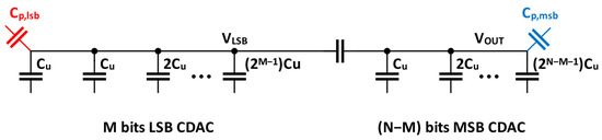
Figure 4.
Parasitic capacitances on a split CDAC.
Second, based on the analysis in Section 2.2, CSCDAC architecture can be designed as , thus simplifying the design process. Instead of , standard split CDAC requires a of to prevent gain error and harmonic distortions. Some studies have modified the LSB CDAC array such that could be used as , but that did not remove the gain error [8].
As a trade-off, the total power consumption of the CSCDAC is higher than the CDAC due to the static power consumption of the CSDAC. Despite that, static power consumption can be optimized. The CSDAC’s static power depends on the full-scale current, while the full-scale current is set by both the full-scale voltage and the termination resistor. The full-scale voltage is fixed for a certain application, and hence, the only variable is the termination resistor. However, the termination resistors and the effective capacitance at the CSDAC output affect the settling time of the CSDAC output voltage. For instance, to have the CSDAC output settled to half the LSB of N-bit resolution, the required RC can be described as follows.
where T is the inverse of the clocking frequency.
To reduce the CSDAC’s static power with a fixed full-scale voltage, the resistance should be maximized. Despite increasing the termination resistance, which reduces the power consumption, it also means that to maintain a certain SFDR, a higher current source output impedance is required. The SFDR is the ratio between the signal power and the highest harmonic distortion. The relationship between the harmonic distortion, termination resistance, and the current source output impedance is described as follows [9].
where is the unit current source output impedance, is the termination impedance, is the number of bits of the CSDAC, and is the order of harmonic distortion.
Figure 5 illustrates the schematic and the equivalent model of a unit CSDAC cell. A high-resolution CSDAC requires the current sources to be well matched. The matching of the MOSFET current sources can be improved by increasing the current source’s overdrive voltage or by increasing the gate area [10]. The gate area of the current source should be optimized to reduce the die area overhead. According to [9], for an N-bit CSDAC, the mismatch of the current sources, which requires the integral-non-linearity (INL) to be lower than 0.5 LSB for a certain yield rate, is expressed below.
where is the current source mismatch and .
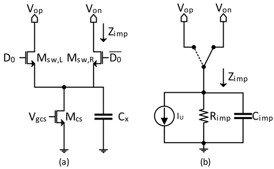
Figure 5.
A unit CSDAC cell: (a) schematic; (b) equivalent model.
To obtain a 99% yield in 12-bit CSDACs, the required current source mismatch should be less or equal to 0.3%. However, for a 6-bit CSDAC integrated into a 12-bit CSCDAC, the required current source mismatch is 2.42%.
3. 12-Bit CSCDAC Design Considerations
First, the settling time of the CSDAC output to half the LSB must be smaller than one conversion period. According to (9), to have the CSDAC output settled to half the LSB within the 0.5 ns, the product of RC must be at most . To fulfill the design constraint, the termination resistance is designed to be 500 Ω when Cu is designed to be 52 fF.
Under low-sampling frequency, the CSCDAC power consumption is mainly contributed by static power consumption from the CSDAC. As mentioned in the previous section, the full-scale current, , is determined by the termination resistor. Therefore, the power consumption from the CSDAC is set by the termination resistance and the full-scale voltage of the LSB CSDAC. In this example, based on (7), the full-scale output voltage of the LSB CSDAC is . The current across the termination resistance is shown below.
Then, the total power consumed by the LSB CSDAC can be described as follows.
Equation (13) supports the statement made in the previous paragraph that increasing the termination resistance reduces the static power consumption in a CSDAC.
According to (10), to obtain an SFDR of 70 dB, the output resistance of a unit CSDAC element must be at least 112.5 kΩ. In this work, the output resistance of the unit CSDAC was designed to be 211 kΩ. Next, by referring to (11), for a 4-bit CSDAC to have a 99% yield, the current source mismatch should be at most 4.84%. The size of the current source MOSFET was designed as W = 5.8 μm, L = 0.4 μm, such that the current mismatch was 3.38%. The current-steering switches were designed to be W = 0.66 μm, L = 0.09 μm. The thermometer switching scheme was applied to ensure the monotonicity of the CSDAC.
Next, the requirement for the capacitor mismatch needs to be considered. To characterize the capacitor mismatch, 3000 Monte Carlo points were run, and the obtained was 0.1%. According to (11), to obtain a 99% yield on an 8-bit CDAC, is required to be less than 1%. The unit capacitance can be designed to be lower than 52 fF to improve the settling time while cutting down the DAC area.
Different CDAC to CSDAC segmentations were also investigated. A 12-bit CSCDAC with various CDAC to CSDAC segmentations was modeled. The parameters of the unit capacitance and the unit current source used in this study follow those mentioned in the previous paragraphs. The 12-bit CSCDAC was simulated at a 2 GS/s sampling frequency to obtain the total power. To understand the power and area trade-off, Figure 6 plots the product of total power and the DAC core area against the CSDAC bit resolution. Although it seems that 6-6 segmentation should be chosen to optimize the total power and area, the model did not keep SFDR to at least 70 dB.
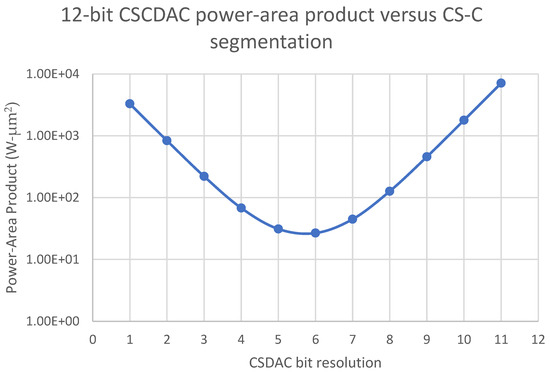
Figure 6.
The 12-bit CSCDAC power-area-product versus CS-C segmentation.
As described in (10), increasing the number of bits taken by the CSDAC requires higher current source output impedance so that the targeted SFDR is not compromised. To achieve the SFDR of 70 dBc while fixing the full-scale voltage and the static power consumption, the required current source output resistance, , versus the estimated CSCDAC can be tabulated in Table 1.

Table 1.
Study of CSCDAC with various segmentation.
Since the 6-6 and 4-8 CDAC to CSDAC segmentation requires the output resistance, , to be near 1 MΩ, it requires the current sources to be cascoded, thus reducing the bandwidth of the output impedance. This work aimed to set the output impedance bandwidth to be as high as possible, and hence, a 12-bit CSCDAC with an 8-4 CDAC-to-CSDAC segmentation was implemented.
Lastly, the layout of the CSCDAC was carefully drawn. The best efforts were paid to equalize the interconnections between the drivers and the pass transistors. For a compact layout, the pass transistors were placed underneath the unit capacitor that they were connected to. The layout diagram of this work is shown in Figure 7. The total area occupied by the CSDAC core and the switch drivers was 0.154 mm2 (440 μm × 350 μm). The total area would have been 0.227 mm2 if the area of the test circuits was included.
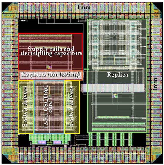
Figure 7.
Layout view of the 12-bit CSCDAC with in-built test circuits.
4. Simulation Results and Discussion
The 12-bit CSCDAC was tested using the test bench shown in Figure 8. The parasitic capacitances of 1 pF were modeled in the test bench. To shorten the simulation time, the test circuits, which comprised a register array, were excluded from this simulation. An ideal 12-bit ADC was used to convert an ideal sine wave with signal frequency to 12-bit words to the CSCDAC. An ideal clock signal was used to set the frequency of the digital words being sampled by the CSCDAC, . and were set to 1 V and 0.5 V, respectively. There were two VDD domains in the CSCDAC block, AVDD, and DVDD, which were both set to 1 V.
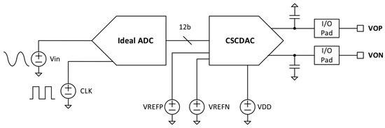
Figure 8.
The simplified schematic of the CSCDAC test bench.
The typical pre-layout simulation showed that at and , the 12-bit CSCDAC exhibited 84 dBc SFDR, 73.66 SNDR, and 11.94 ENOB. The Monte Carlo simulation was executed to factor in the DAC element mismatches. Under 2 GS/s clocking frequency, two signal frequencies were used in the Monte Carlo simulations, and they were 109.375 MHz and 953.125 MHz, which represents the signal-to-sampling ratio, , of 7/128 and 61/128, respectively. In total, 200 sample points in the Monte Carlo simulation were run. The worst-case results are tabulated in Table 2.
Table 2.
Worst case Monte Carlo pre-layout performance at fsig = 109.375 MHz and 953.125 MHz.
The post-layout simulation on the parasitic RC-extracted CSCDAC core was carried out to obtain a more realistic performance. The post-layout simulation results are tabulated in Table 3 below.
Table 3.
The 12-bit CSCDAC post-layout performance at fsig = 109.375 MHz and 953.125 MHz.
The post-layout simulation shows that the CSCDAC linearity degraded by about 1 ENOB compared to the pre-layout simulation. The main degradation was found to be contributed by the layout of the MSB CDAC. The possible cause of this phenomenon is the mismatch among the interconnects that lead to each of the CDAC elements. This includes the interconnects from the digital inputs, references, and the power supply. When there is a mismatch among the interconnects, the error contributed by each bit is different, and thus the error will be code-dependent. The post-layout performance should be improved if the parasitic resistance and capacitance of the interconnect are equalized.
The average power consumption of the 12-bit CSCDAC is about 54 mW at 2 GS/s, with 1 mW contributed by the LSB CSDAC and 53 mW from the 8-bit MSB CDAC. The power consumption from the 8-bit MSB CDAC can be calculated using the equation of dynamic power consumption shown below.
The bit resolution of the capacitive sub-DAC is 8 bits, and the unit capacitance was designed to be 52 fF, with the total capacitance in the differential 8-bit CDAC at 26.52 pF. Therefore, at 2 GS/s sampling frequency, the average dynamic power consumption from the CDAC was 53 mW.
Lastly, the post-simulated results were tabulated and compared with other work in Table 4 as shown below. The work in [11] can achieve a higher SFDR with a lower DAC area as the stochastic switching scheme named dynamic element matching and digital-return-to-zero (DEMDRZ) was adopted to remove the output code dependency that causes non-linearity. The total power consumption in [12] was higher than the one reported in this work, not only because the DAC was operating at a higher sampling frequency but also because the DAC provides a higher full-scale current. The full-scale current was 50 mA to allow the output to swing at . The work in [13] had a higher power consumption compared to the other work shown in the table, as the sampling frequency was about five times higher than the other work. The SFDR also decreases with the increase in sampling and signal frequency due to the finite output impedance of the current sources.
Table 4.
Comparison with other work.
5. Conclusions
A novel 12-bit current-steering–capacitive digital-to-analog converter (CSCDAC) is presented in this paper. The post-layout simulation results show that the CSCDAC operates at 2 GS/s with a 67.62 dBc worse SFDR while consuming 54 mW of total power at the Nyquist data rate. The stochastic switching scheme and optimal combination algorithms (OCAs) can be integrated into this CSCDAC architecture to improve DAC linearity. Switching schemes such as dynamic element matching (DEM) randomize the error from each of the DAC elements, preventing the same error from appearing periodically and, thus, reducing the harmonic distortion, which degrades the dynamic linearity. The static linearity of the DAC can be improved by applying OCAs. OCAs identify the mismatch of DAC elements and compute the optimal switching sequence to minimize INL [14,15].
Author Contributions
Conceptualization, X.Y.L. and B.C.T.T.; methodology, X.Y.L., B.C.T.T., V.N. and W.C.L.; software, X.Y.L., B.C.T.T. and W.C.L.; validation, X.Y.L.; formal analysis, X.Y.L.; investigation, X.Y.L.; resources, X.Y.L.; data curation, X.Y.L.; writing—original draft preparation, X.Y.L.; writing—review and editing, B.C.T.T., V.N., W.C.L. and L.S.; visualization, X.Y.L.; supervision, L.S.; project administration, X.Y.L.; funding acquisition, L.S. All authors have read and agreed to the published version of the manuscript.
Funding
MediaTek Singapore Pte. Ltd. funded the fabrication of the design.
Data Availability Statement
The original contributions presented in this study are included in the article. Further inquiries can be directed to the corresponding author(s).
Acknowledgments
The authors would like to thank MediaTek Singapore Pte. Ltd. for supporting the design.
Conflicts of Interest
The author B. C. T. Teo was employed by the company Silicon Labs Singapore. The author W. C. Lim was employed by the company STMicroelectronics Asia Pacific Pte. Ltd. The author N. Venkadasamy was employed by the company CM Engineering Labs Singapore Ptd. Ltd. The remaining authors declare that the research was conducted in the absence of any commercial or financial relationships that could be construed as potential conflicts of interest. The funder did not participate in the design of the study.
References
- Baker, R. CMOS: Circuit Design, Layout, and Simulation, 3rd ed.; Wiley: Hoboken, NJ, USA, 2010; Volume 18. [Google Scholar] [CrossRef]
- Ahuja, A.; Badami, K.; Barbelenet, C.; Emery, S. Comparison of Capacitive DAC Architectures for Power and Area Efficient SAR ADC Designs. In Proceedings of the 2021 IEEE International Symposium on Circuits and Systems (ISCAS), Daegu, Republic of Korea, 22–28 May 2021; pp. 1–5. [Google Scholar] [CrossRef]
- Maloberti, F. (Ed.) Nyquist-Rate Digital to Analog Converters. In Data Converters; Springer: Boston, MA, USA, 2007; pp. 77–140. [Google Scholar] [CrossRef]
- Kim, J.; Jang, W.; Lee, Y.; Kim, W.; Oh, S.; Lee, J.; Choi, J.; Chun, J.-H.; Cho, T.B. Design and Analysis of a 12-b Current-Steering DAC in a 14-nm FinFET Technology for 2G/3G/4G Cellular Applications. IEEE Trans. Circuits Syst. I Regul. Pap. 2019, 66, 3723–3732. [Google Scholar] [CrossRef]
- Gruber, D.; Clara, M.; Sanchez, R.; Wang, Y.-S.; Duller, C.; Rauter, G.; Torta, P.; Azadet, K. 10.6 A 12b 16GS/s RF-Sampling Capacitive DAC for Multi-Band Soft-Radio Base-Station Applications with On-Chip Transmission-Line Matching Network in 16 nm FinFET. In Proceedings of the 2021 IEEE International Solid-State Circuits Conference (ISSCC), San Francisco, CA, USA, 13–22 February 2021; pp. 174–176. [Google Scholar] [CrossRef]
- Li, Y. Improved binary-weighted split-capacitive-array DAC for high-resolution SAR ADCs. Electron. Lett. 2014, 50, 1194–1195. [Google Scholar] [CrossRef]
- Zhang, Q.; Li, J.; Zhang, Z.; Wu, K.; Ning, N.; Yu, Q. A Low-Power and Area-Efficient 14-bit SAR ADC with Hybrid CDAC for Array Sensors. In Proceedings of the 2019 IEEE International Symposium on Circuits and Systems (ISCAS), Sapporo, Japan, 26–29 May 2019; pp. 1–5. [Google Scholar] [CrossRef]
- Zhang, Y.; Bonizzoni, E.; Maloberti, F. Mismatch and parasitics limits in capacitors-based SAR ADCs. In Proceedings of the 2016 IEEE International Conference on Electronics, Circuits and Systems (ICECS), Monte Carlo, Monaco, 11–14 December 2016; pp. 33–36. [Google Scholar] [CrossRef]
- van den Bosch, A.; Steyaert, M.; Sansen, W.M.C. Static and Dynamic Performance Limitations for High Speed D/A Converters. In Kluwer International Series in Engineering and Computer Science: Analog Circuits and Signal Processing; Springer: Boston, MA, USA, 2015. [Google Scholar]
- Pelgrom, M.; Duinmaijer, A.; Welbers, A. Matching properties of MOS transistors. IEEE J. Solid-State Circuits 1989, 24, 1433–1439. [Google Scholar] [CrossRef]
- Lin, W.-T.; Huang, H.-Y.; Kuo, T.-H. A 12-bit 40 nm DAC Achieving SFDR > 70 dB at 1.6 GS/s and IMD < –61dB at 2.8 GS/s With DEMDRZ Technique. IEEE J. Solid-State Circuits 2014, 49, 708–717. [Google Scholar] [CrossRef]
- Lin, C.-H.; van der Goes, F.M.L.; Westra, J.R.; Mulder, J.; Lin, Y.; Arslan, E.; Ayranci, E.; Liu, X.; Bult, K. A 12 bit 2.9 GS/s DAC With IM3 ≪ -60 dBc Beyond 1 GHz in 65 nm CMOS. IEEE J. Solid-State Circuits 2009, 44, 3285–3293. [Google Scholar] [CrossRef]
- Huang, H.-Y.; Kuo, T.-H. A 0.07-mm2 162-mW DAC Achieving >65 dBc SFDR and < −70 dBc IM3 at 10 GS/s with Output Impedance Compensation and Concentric Parallelogram Routing. IEEE J. Solid-State Circuits 2020, 55, 2478–2488. [Google Scholar] [CrossRef]
- Gagliardi, F.; Scintu, D.; Piotto, M.; Bruschi, P.; Dei, M. Static-Linearity Enhancement Techniques for Digital-to-Analog Converters Exploiting Optimal Arrangements of Unit Elements. IEEE Trans. Very Large Scale Integr. Syst. 2024, 32, 2243–2256. [Google Scholar] [CrossRef]
- Fan, H.; Li, J.; Maloberti, F. Order Statistics and Optimal Selection of Unit Elements in DACs to Enhance the Static Linearity. IEEE Trans. Circuits Syst. I Regul. Pap. 2020, 67, 2193–2203. [Google Scholar] [CrossRef]
Disclaimer/Publisher’s Note: The statements, opinions and data contained in all publications are solely those of the individual author(s) and contributor(s) and not of MDPI and/or the editor(s). MDPI and/or the editor(s) disclaim responsibility for any injury to people or property resulting from any ideas, methods, instructions or products referred to in the content. |
© 2025 by the authors. Licensee MDPI, Basel, Switzerland. This article is an open access article distributed under the terms and conditions of the Creative Commons Attribution (CC BY) license (https://creativecommons.org/licenses/by/4.0/).