Abstract
The paper describes the design and implementation of power management circuits for RF energy harvesters suitable for integration in wireless sensor nodes. In particular, we report the power management circuits used to provide the voltage supply of an integrated temperature sensor with analog-to-digital converter. A DC-DC boost converter is used to transfer efficiently the energy harvested from a generic radio-frequency rectifier into a charge reservoir, whereas a linear regulator scales the voltage supply to a suitable value for a sensing and conversion circuit. Implemented in a 65 nm CMOS technology, the power management system achieves a measured overall efficiency of 20%, with an available power of 4.5 W at the DC-DC converter input. The system can sustain a temperature measurement rate of one sample/s with an RF input power of −28 dBm, making it compatible with the power levels available in generic outdoor environments.
1. Introduction
Energy Harvesting from the Electro-Magnetic (EM) field in the Ultra-High frequency (UHF) range is one of the most promising techniques that will further push the penetration of wireless sensor nodes (WSN) in several environments [1,2,3,4]. One the one hand, harvesting from RF sources requires neither movements, like in piezoelectric and mechanical harvesters, nor thermal gradients, like in thermo-electric harvesters that can limit the system lifetime and the harvesting efficiency. On the other hand, the large variability in space and time of the available EM power represents a significant challenge for the complete enabling of this source in the WSN scenario [5,6,7,8]. The front-end block of any RF harvester is the RF rectifier connected to the antenna terminals and used to perform the AC-to-DC power conversion [9]. Considering the large variability of the RF source, an energy reservoir is also usually included in the system to accumulate the collected energy. In the RF harvesting for WSN contest, a Power Management Unit (PMU) is mandatory to stock the energy harvested from the environment in the reservoir and also to supply the circuits of the sensor node. The main purposes of the PMU are the contemporary maximization of the amount of energy transferred from the antenna to the reservoir, and the proper and efficient regulation of the supply voltage of the sensor node from the harvested energy.
A PMU acting as interface between a generic RF rectifier and an integrated temperature sensor is presented in this paper. The system is composed by a DC-DC converter, for the optimization of the energy transfer from the output of the RF rectifier to the accumulator, and a low drop-out linear voltage regulator (LDO), for the generation of the voltage supply of the sensor. The former circuit is an input-driven boost converter specifically designed for intermittent energy sources and is thus well matched with the RF energy harvesting contest. The LDO, based on an integrated bandgap reference and an operational amplifier, scales the voltage of the accumulator to a suitable value for the WSN circuits [10]. The control strategy sets the DC-DC input voltage, which corresponds to the output voltage of the rectifier. This feature, together with the extreme low power consumption of the whole PMU, allows the positive energy transfer to the reservoir for very low value of RF incoming power. Moreover, the adoption of this control strategy permits including in the system a Maximum Power Point Tracking circuit acting on the input voltage of the DC-DC converter, which is fundamental for the maximization of the collected energy from discontinuous energy sources [11]. The PMU and the temperature sensor were implemented in a test chip in 65 nm CMOS technology.
Measurement results demonstrate that the proposed PMU achieves a temperature measurement rate of 1 Sample/s, with an RF input power of dBm, if interfaced to an RF rectifier featuring 30% of power efficiency [12,13], corresponding to 395 nW delivered to the DC-DC converter. Therefore, this PMU can be effectively used in the context of RF harvesting thanks to its inherent low power consumption and the suitable power efficiency.
This paper is organized as follows. In the next section, the generation of the voltage supply for an integrated sensor from the EM power is discussed, focusing both on the circuits composing the architecture of the PMU and on the fundamental equations. Measurement results on silicon samples in 65-nm CMOS technology are reported in Section 3.
2. System Description
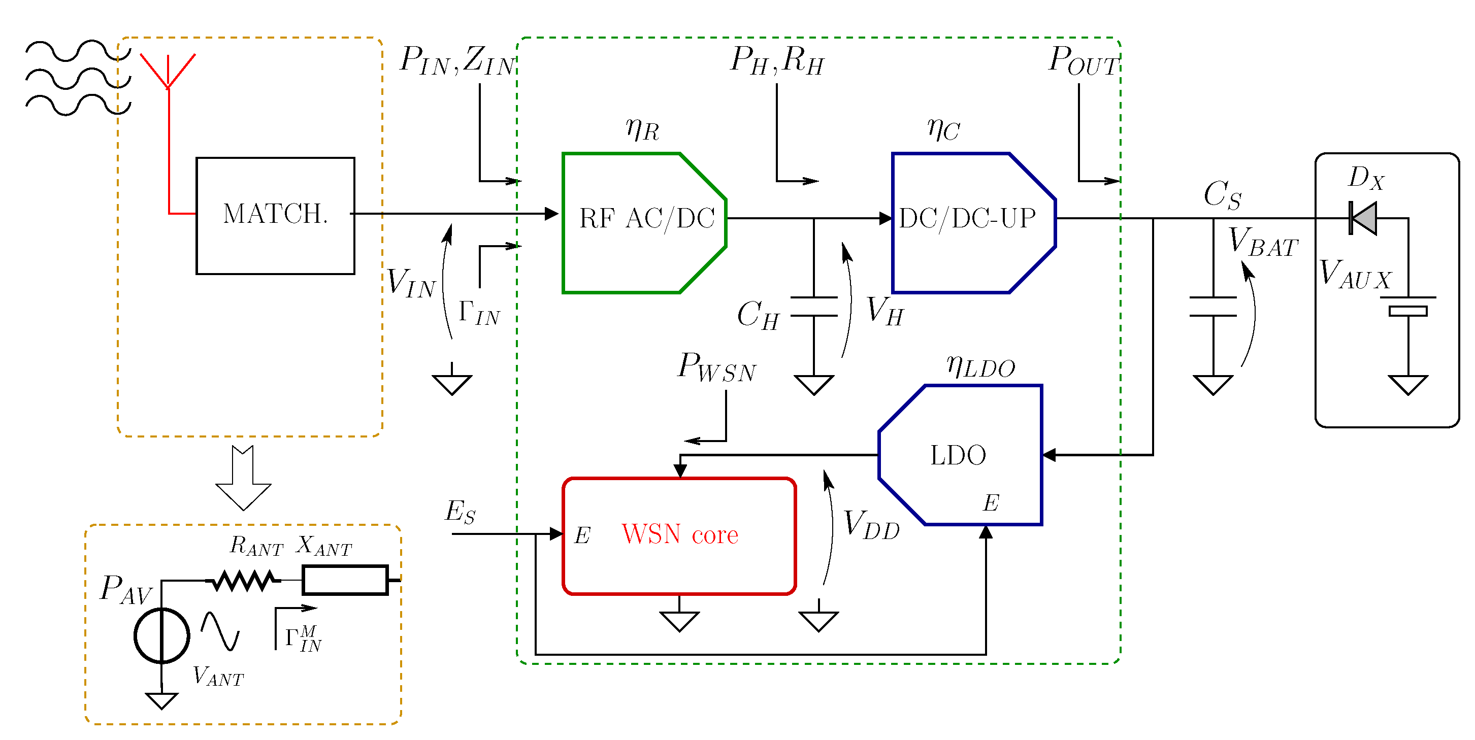
The black-box schematic of a typical WSN with RF energy harvesting is shown in Figure 1. At the resonance frequency, the antenna is modeled with a lumped-elements circuit including a voltage source and a series resistance . A matching network between the antenna and the input terminals of the harvester is mandatory to match the impedance of the two circuits and achieve the power matching condition. In the model of Figure 1, the matching reactance is introduced in series with the input impedance of the harvester, . The full and reactive power matching conditions at the center-band signal frequency are:
where is the reflection coefficient at the left terminal of the matching reactance :
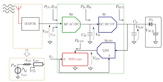
Figure 1.
Black-box schematic of a WSN with RF energy harvesting and power management circuits.
The condition in (2) corresponds to the power matching limited to only the reactive part of the input impedance.
The front-end block of the harvester is an RF-rectifier, which performs the AC-to-DC power conversion [9,12,14,15]. Thus, considering a single-tone with frequency at the antenna terminal, the DC voltage at the rectifier output is:
where is the amplitude of the sine wave at the rectifier input, and is the rectifier threshold. Across a typical RF power range, exhibits a negative reactance [9], which may be matched with an equivalent series inductance . It is worth noticing that such tuning equivalent inductance can be synthesized by slightly shifting the center frequency of the antenna from the signal frequency. Assuming reactive matching, the following analytic expressions are obtained from circuit analysis [8]:
where is the rectifier input resistance, and is the quality factor of the R-L-C series network involving the antenna and rectifier resistance, and , respectively, the rectifier input capacitance , and the matching inductance :
where . The equivalent input capacitance at the frequency is:
In RF energy harvesters, the center-band frequency must be tuned to compensate for the variability of the Electro-Magnetic spectrum with the location and the time. The reactive matching condition can be obtained by means of a programmable bank of integrated capacitors connected to the rectifier input terminals [16,17].
In the calculation of the power delivered by the rectifier , and of the DC output voltage , it has to be considered that the rectifier input power depends on the rectifier input resistance , assuming that the reactive matching condition in (2) is satisfied. Furthermore, the power delivered by the rectifier to the DC/DC converter is set by and by the rectifier efficiency . The influence of on is due to the internal power consumption effects into the rectifier. At low values of input power, the efficiency is mainly set by the nonlinearity of the series resistance of the rectifying device [18] and by the internal consumption of the threshold compensation circuits, when present [19]. On the contrary, at high power levels, is mainly limited by the voltage drop across the rectifying device and its series resistance [11]. Moreover, the average output voltage at the steady-state has a significant impact on both and values [8,11]. Therefore, with the lumped-elements model in [11] , , and are obtained from , , and as independent variables, where is the equivalent load resistance of the rectifier.
In the design of the RF scavenging system, the large variability of the EM power in the considered frequency band must be taken into account. Indeed, the largest amount of EM power in the UHF bands is provided by the discontinuous transmissions from base stations of the cellular phone services, which also exhibits the higher density in the urban environment [6,7,8]. Therefore, the harvester must properly handle the case of intermittent available RF power that may fall below the minimum value required to supply the WSN circuits. These events can occur several times per day and for long-lasting periods of time. Thus, in the system of Figure 1, the harvested RF energy is transferred to an energy reservoir, corresponding to an off-chip large capacitor . In a fully-autonomous scavenging system, the WSN circuits (analog, digital, and RF) are supplied with the energy accumulated in the reservoir, provided that is higher than the minimum operative supply voltage of those circuits. If an auxiliary battery is added to the system, as in the box on the right side of Figure 1, the RF harvester will extend the battery lifetime, provided sufficient RF power is available. In the latter scenario, when drops below , being the forward voltage of diode , the auxiliary battery supplies the WSN circuits and inhibits the further discharge of the reservoir. A more power-efficient solution could be implemented with a series switch and a low-power comparator.
In the system of Figure 1, the harvested energy is maximized with the simultaneous maximization of the output voltage . Due to this constraint and to the large variability of the available RF power, the RF rectifier should not be directly connected to the main reservoir. Indeed, with a low input power, the rectifier is not able to transfer energy to the reservoir, whereas the maximization of the rectifier efficiency requires to set the rectifier output voltage at the optimum value, which depends on the input power [11]. Therefore, a DC-DC converter with an intermediate energy reservoir is introduced between the rectifier and the main reservoir .
2.1. DC-DC Converter with Input-Control
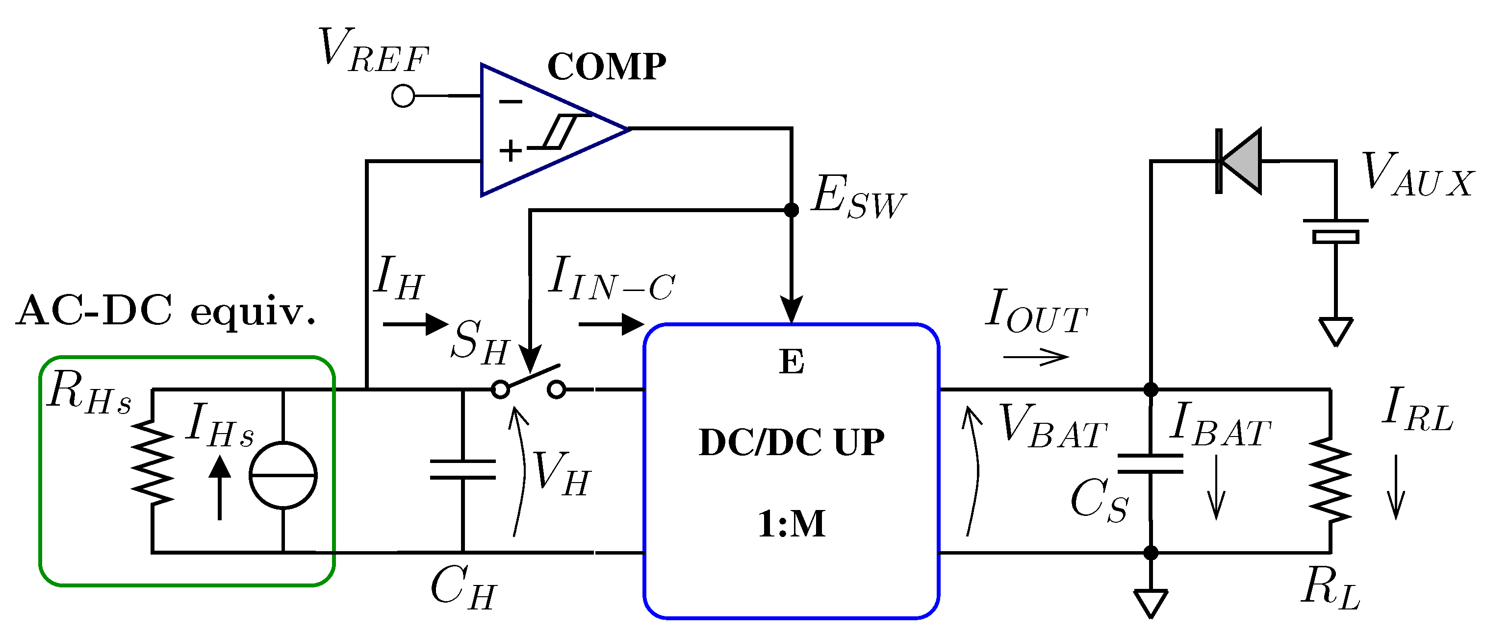
The proposed RF energy harvesting system is shown in Figure 2. The RF rectifier is modeled with the Norton equivalent, based on the short-circuit current source and the small-signal output resistance . It has to be noticed that this model is valid at constant input power and output voltage . As it is explained below, the latter condition can be achieved with good approximation in the system of Figure 2, with no dependency on the RF input power value. The on-chip capacitor at the input of the DC-DC converter is the intermediate energy reservoir. The step-up converter is controlled by means of the hysteretic comparator COMP that monitors the voltage at the rectifier output and drives the switch . In the proposed system, as long as the rectifier output voltage is lower than the set-point value , the DC-DC converter is disabled and disconnected from the rectifier. Therefore, if is higher than the internal power consumption of the rectifier, the charge flux from the rectifier to the intermediate reservoir pushes up the output voltage . When the threshold voltage is crossed, the DC-DC converter is enabled and connected to the intermediate charge reservoir . Thus, a packet of energy is transferred to the main reservoir and the voltage at the rectifier output drops suddenly, unless the incoming power can fully sustain the average input current . The activation of the converter requires that the asymptotic value of in the open-load condition is higher than the comparator threshold, introducing a lower bound for the RF input power to enable a net energy transfer from the antenna to the DC-DC converter.
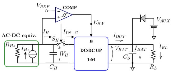
Figure 2.
RF Energy harvester system based on a RF rectifier and an input-controlled DC-DC converter.
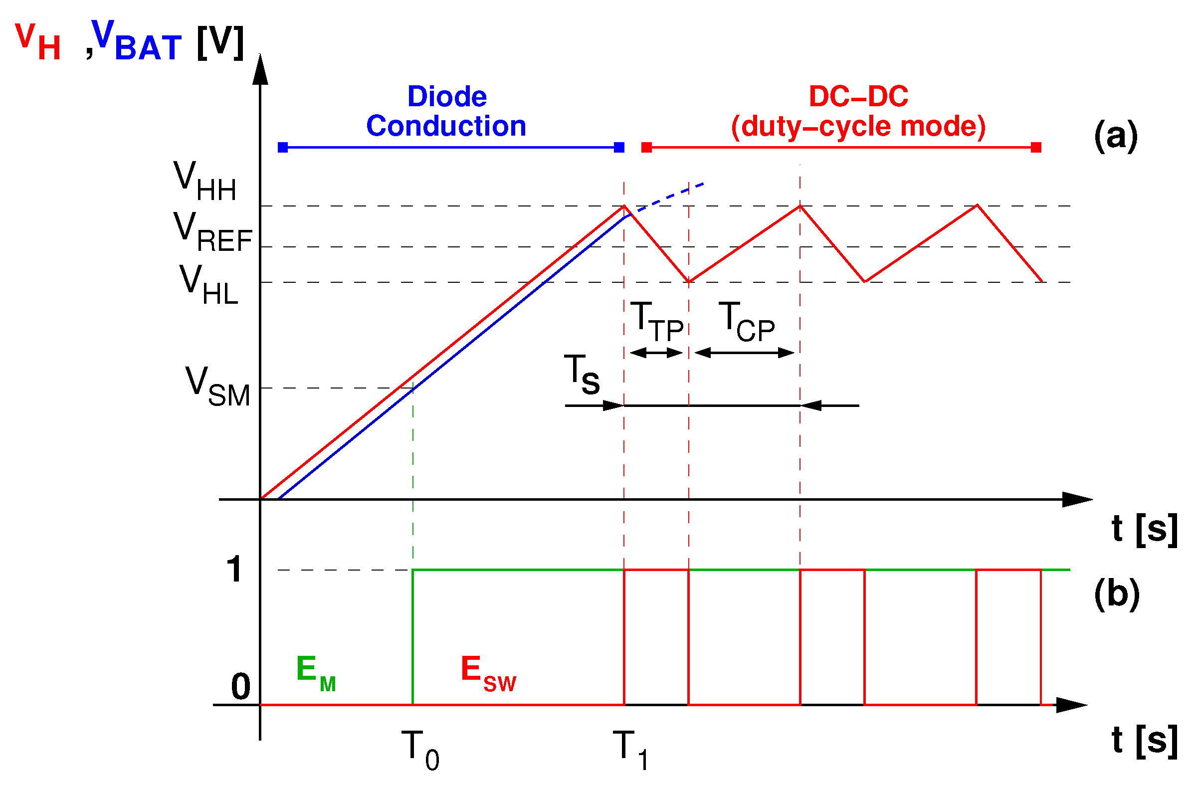
The waveforms of and of the control signal for an autonomous energy harvesting system, without an auxiliary battery, are shown in Figure 3. Here, is the time period of a complete cycle that is divided into the energy transfer phase (converter on), with length , and the recharging phase (converter off), with length . The input–output voltage ratio of the DC-DC converter in open-load condition (M) must be optimized on the basis of the following design constraints:
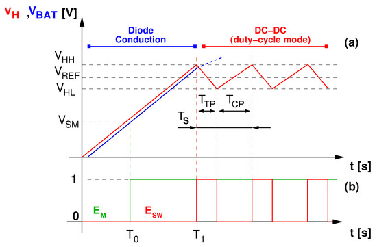
Figure 3.
(a) time graph of the output voltage of the rectifier output (red trace) and of (blue trace) for moderate-to-low input power; (b) control signal of switch in Figure 2 (green trace) and enables the signal of the DC-DC converter (red trace).
- Maximization of the DC-DC converter efficiency
- Maximization of the energy that can be stored in the reservoir .
The second constraint requires the maximization of the output voltage at the steady-state. However, the maximum voltage that can be tolerated at the converter output depends on the breakdown voltage of the MOS devices connected to the output port. In a sub-100 nm technology, the available thick-oxide devices usually exhibit a breakdown voltage within 3.3 V. Furthermore, it is worth noticing that the converter efficiency usually decreases at increasing values of the voltage ratio, thus setting a further constraint on the maximum output voltage.
In the schematic view of the harvester in Figure 2, the output voltage can be considered approximately constant and not dependent on the power delivered by the DC-DC converter. This assumption holds in a time window that includes several recharge-and-transfer periods of the converter, provided that the rate-of-change of is sufficiently low. The low derivative of the battery voltage is due to the high value of the reservoir capacitance, which can be either a multilayer surface-mounting (SMD) ceramic capacitor or a super-capacitor, and it holds considering the ultra-low value of RF available power in generic environments. Cost and size are fundamental parameters for the choice of the energy reservoir, as well as the value of the insulation resistance, setting the self-discharge current. Low-leakage super capacitors exhibit a leakage current in the microampere range [20], whereas the insulation resistance of an SMD ceramic capacitor, with X7R dielectric, is higher than 100 F, leading to a discharge current lower than 100 nA at 2.5 V output [21]. It is worth noticing that SMD ceramic capacitors in the 1-to-10 F range are available in the 0603 size. Considering the low average value of the available RF power, the recharge output current may be lower than the self-discharge current of a super capacitor for a large fraction of the time, thus nullifying the benefits of the RF energy scavenging. Therefore, a ceramic capacitor is the preferred choice, given that the energy required by the WSN, when it is enabled, can be provided by a microfarad capacitor with an acceptable voltage drop.
Since the DC-DC converter is loaded by a large capacitor and thus operates with an almost constant output voltage, a reverse energy flow from to the rectifier output occurs if the converter is activated with lower than . Therefore, the following condition must be fulfilled for the lower threshold of the hysteretic comparator:
An approximate analytic expression of the input resistance of a converter with controlled input voltage is obtained from the assumption of a negligible voltage ripple affecting , shown in Figure 3:
where has been approximated with its average value. Therefore, with the input control, the equivalent input resistance of the DC-DC converter is dynamically adapted to the RF input power. It is worth noticing that the equivalent load resistance , at a given RF input power level, depends on the set-point control voltage . Thus, the rectifier efficiency can be maximized at each input power condition by setting the optimum value of and by changing the converter voltage ratio M accordingly. This optimization must be implemented in real-time mode and requires a maximum power point tracking (MPPT) system [11].
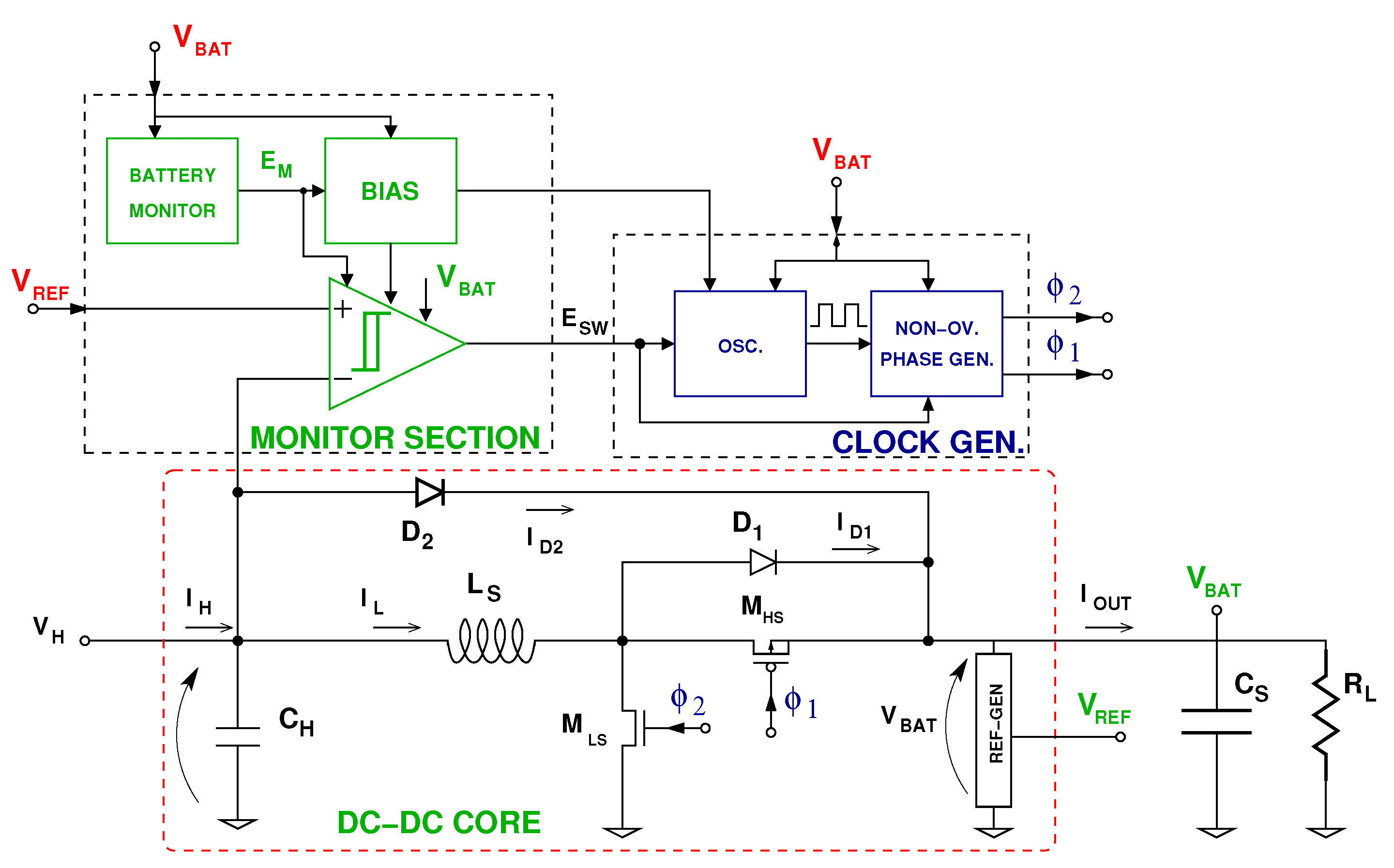
The circuit schematic of the DC-DC converter in the proposed harvester implementation is shown in Figure 4, where the only off-chip component is the inductor . A boost converter with external high-Q inductance and working in the Continuous Conduction Mode (CCM) was preferred for the higher efficiency and the smaller silicon area than switched-capacitors’ converters. It is worth noticing that, in spite of the higher switching frequency compared to boost converters working in the Discontinuous Conduction Mode (DCM) or Boundary Mode [22], the control circuit of CCM converters exhibits lower complexity and power consumption.
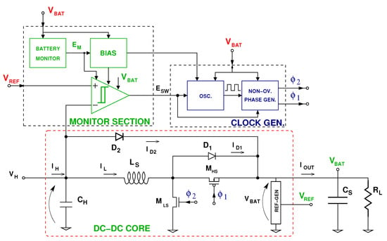
Figure 4.
Circuit schematic of the DC-DC converter with input control.
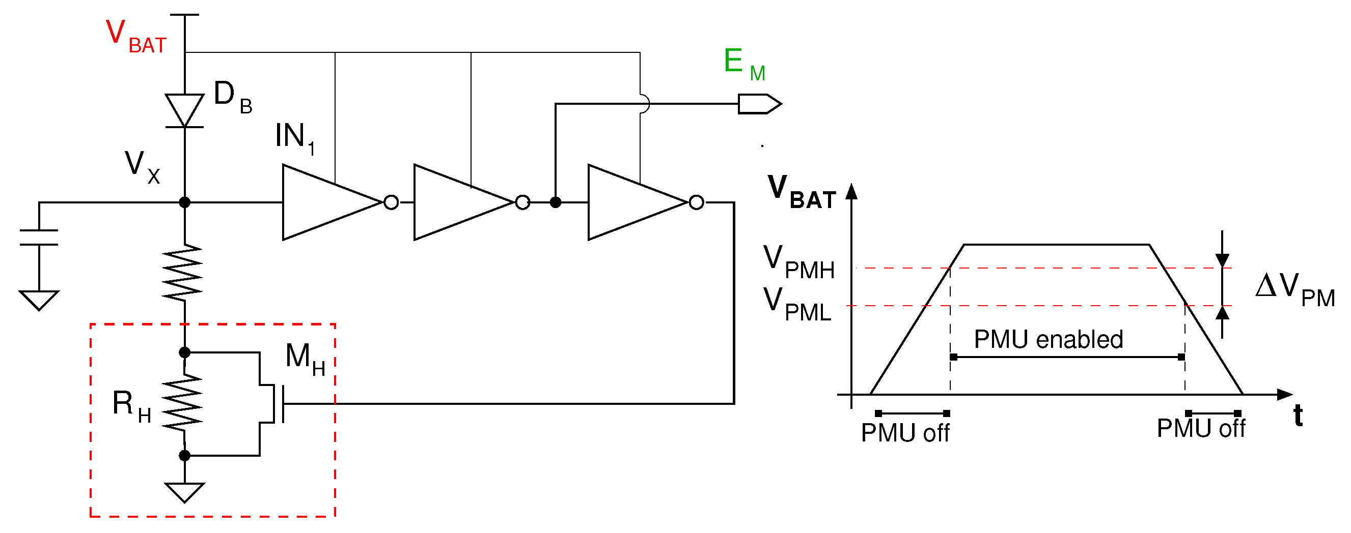
The converter is based on the sections shown in Figure 4: the monitor, the clock generator, and the core converter. In the first block, at the top-left of the circuit schematic, a battery monitor circuit enables the comparator and the bias current generator only if the battery voltage is higher than the minimum value that is required by the control circuits (i.e., comparator, bias generator, and oscillator), in Figure 3.
The battery monitor is the only circuit, with the REF-GEN in the converter core, is always supplied by the charge reservoir , and it must be designed for the minimum current consumption. In the circuit schematic of Figure 5, is shifted down by the forward voltage of , i.e., , and compared to the threshold voltage of the CMOS inverter , . Thus, an approximate analytic expression for is obtained:
where in (12) depends on the aspect ratios of the PMOS and NMOS device in . The hysteresis is introduced with transistor . By shorting , increases the diode bias current. Consequently, the voltage drop also increases when the voltage is higher than the threshold of the CMOS inverter.
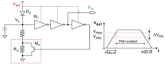
Figure 5.
Circuit schematic of the supply monitor.
The comparator is based on a differential CMOS amplifier with cross-coupled load and a class-AB complementary output stage. If the battery-monitor returns a low output signal, , the comparator is driven in power-off mode and its output is set low, as shown in the time graph at the bottom of Figure 3. On the contrary, with the voltage of the main reservoir higher than the threshold set by the voltage monitor, the comparator is activated. If is lower than the set-point voltage , the clock generation circuits are driven in power-down mode with the outputs and set high and low respectively, in order to switch off both and in the converter core. Thus, in this configuration, the converter is disconnected from both reservoirs and .
The clock generation section includes a ring oscillator, based on current starved CMOS inverters, and a generator of clock signals with non-overlapped phases, driving the MOS switches in the converter section, i.e., and , respectively. The non-overlapping condition is mandatory to ensure that the main reservoir is never shorted to the ground potential through and . The voltage ratio of the converter is set by the duty-cycle of the clock signal, whereas the efficiency is limited by the series resistance of the off-chip inductor , by the on-resistance of the MOS switches, and by the power consumption of the monitor and clock-generation circuits.
Two diodes are added to the circuit: is the free-wheeling diode for the inductor , whereas connects the RF rectifier to the external charge reservoir, and it is activated when is higher than the voltage of the reservoir . This occurs in the case of an excessive available power at the rectifier input or with a battery voltage lower than the threshold of the battery monitor. In the former case, implements the function of voltage limiter at the rectifier output and protects the RF circuit against the over-voltage condition by steering the RF power directly to the main charge reservoir. In the latter case, the power delivered by the rectifier is steered to the main reservoir, bypassing and the series switch. This situation corresponds to the “Diode Conduction” condition in Figure 3.
The REF-GEN block is a voltage divider based on a stack of diode-connected MOS transistors biased in the deep weak-inversion region. Thus, the set-point voltage of the input-control tracks the voltage of the main reservoir. This is mandatory to always comply condition (9) in order to inhibit the reverse energy flow.
The component values of the integrated DC-DC converter are reported in Table 1. The SMD inductor exhibits a series resistance of 40 and a minimum self resonance frequency (SRF) of 2 MHz [23]. The frequency of the DC-DC oscillator, , is set to 750 kHz with a 50% duty-cycle. This leads to an open-load input–output voltage ratio M equal to 2. The value of the integrated capacitor is sized to have at least one converter switching period, , over the process and temperature corner space. Finally, the comparator is designed for 250 mV of hysteresis width , whereas the circuit generating the set-point reference is sized for a typical -over- ratio of 0.65 V/V.

Table 1.
DC-DC converter: design specifications and values of components.
2.2. Linear Regulator
A voltage regulator is usually required to supply the WSN circuits with the available energy of the main reservoir. Indeed, in the system of Figure 1, may decrease down to the threshold voltage for the activation of the auxiliary supply, i.e., . Furthermore, if the WSN circuits are implemented with core MOS devices, their breakdown voltage is approximately 1.2 V or even lower in sub-100 nm technology nodes. Therefore, the WSN circuits cannot be directly supplied by means of the main reservoir and a step-down DC-DC down converter is required.
A DC-DC buck converter would lead to the maximum power efficiency, but it requires an additional off-chip inductor, leading to higher costs and increased area of the printed circuit board (PCB). For this reason, in this prototype, a low-dropout linear regulator (LDO) was preferred.
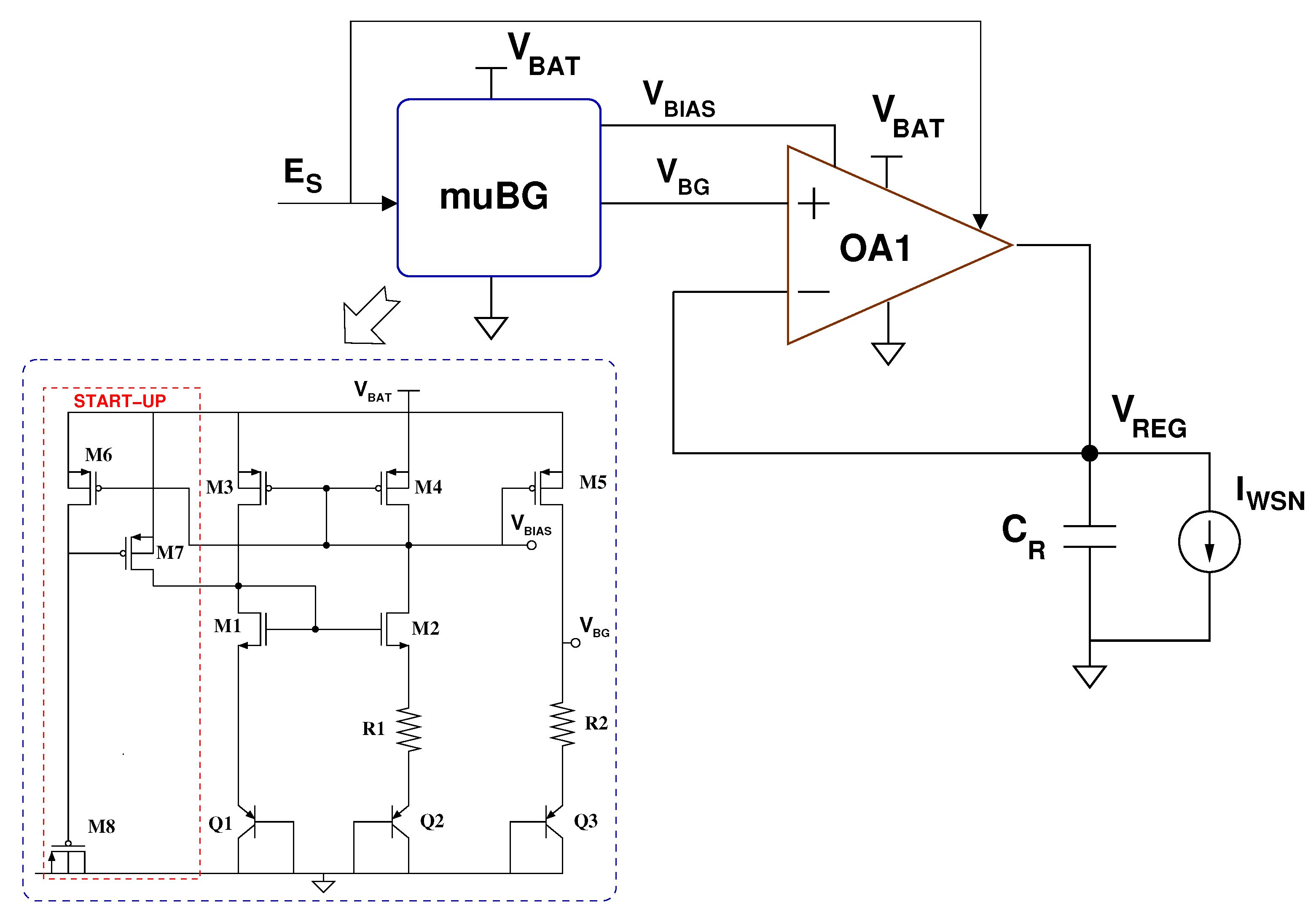
As shown in the circuit schematic of Figure 6, the LDO is based on a bandgap reference, a two-stage operational amplifier without Miller compensation, and the on-chip capacitor . The schematic of the bandgap reference is shown in the dashed box of Figure 6. The voltages at the emitter of and at the upper terminal of are held approximately equal by and , which exhibit the same aspect ratio and equal currents, considering the 1:1 current ratio of the - mirror. Since the emitter area of pnp bipolar junction transistor (BJT) is N times, the emitter area of , the voltage across , and thus the drain current of are proportional to the absolute temperature (PTAT). This PTAT current is mirrored in the left branch of the circuit where a PTAT voltage is generated across resistor and summed up to the emitter-base forward voltage of to generate a reference voltage with zero temperature coefficient at the room temperature (RT). The circuit highlighted in the red box in Figure 6 is the start-up circuit. At the power-on, the MOS capacitor is fully discharged and, consequently, provides a supplementary bias current to . Thus, the circuit bias is moved far from the undesired condition, i.e., and with negligible drain currents. Furthermore, the gate voltage of , , is used to locally generate the opamp bias current. The large on-chip capacitor is mandatory to achieve the required stability margin for the LDO and to limit the ripple affecting the regulated voltage, if the LDO drives circuits with a significant switching activity, like logic gates and switched-capacitors’ circuits.
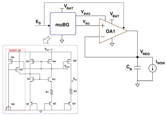
Figure 6.
Circuit schematic of the 1.2 V low-dropout regulator with bandgap reference (dashed blue box).
3. Silicon Implementation and Measurements’ Results
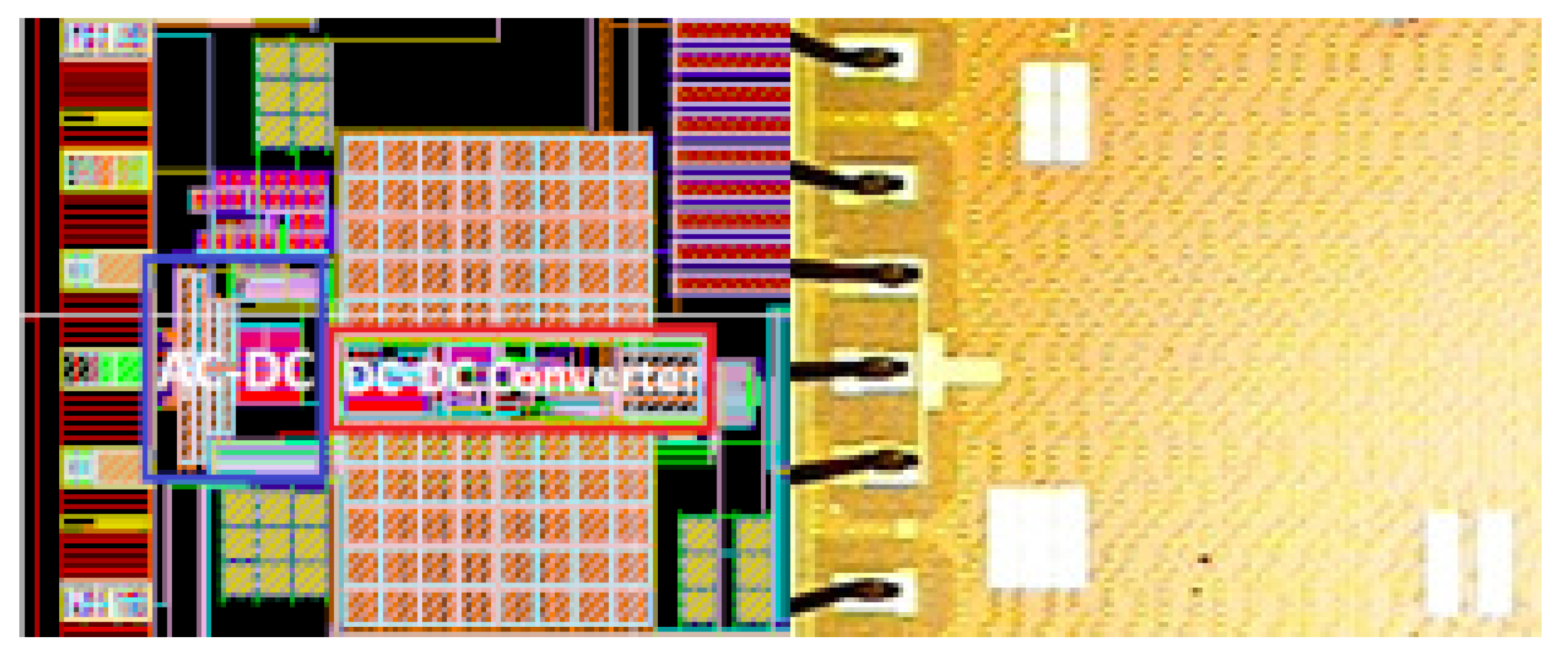
The proposed power-management modules were implemented in 65 nm CMOS technology. The photograph of the test chip is shown in Figure 7 together with the layout.
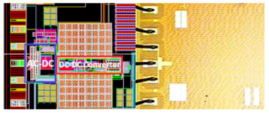
Figure 7.
(Left) layout of the test chip; (Right) photograph of the test chip. The AC-DC and the DC-DC converters are highlighted with the blue and red boxes, respectively.
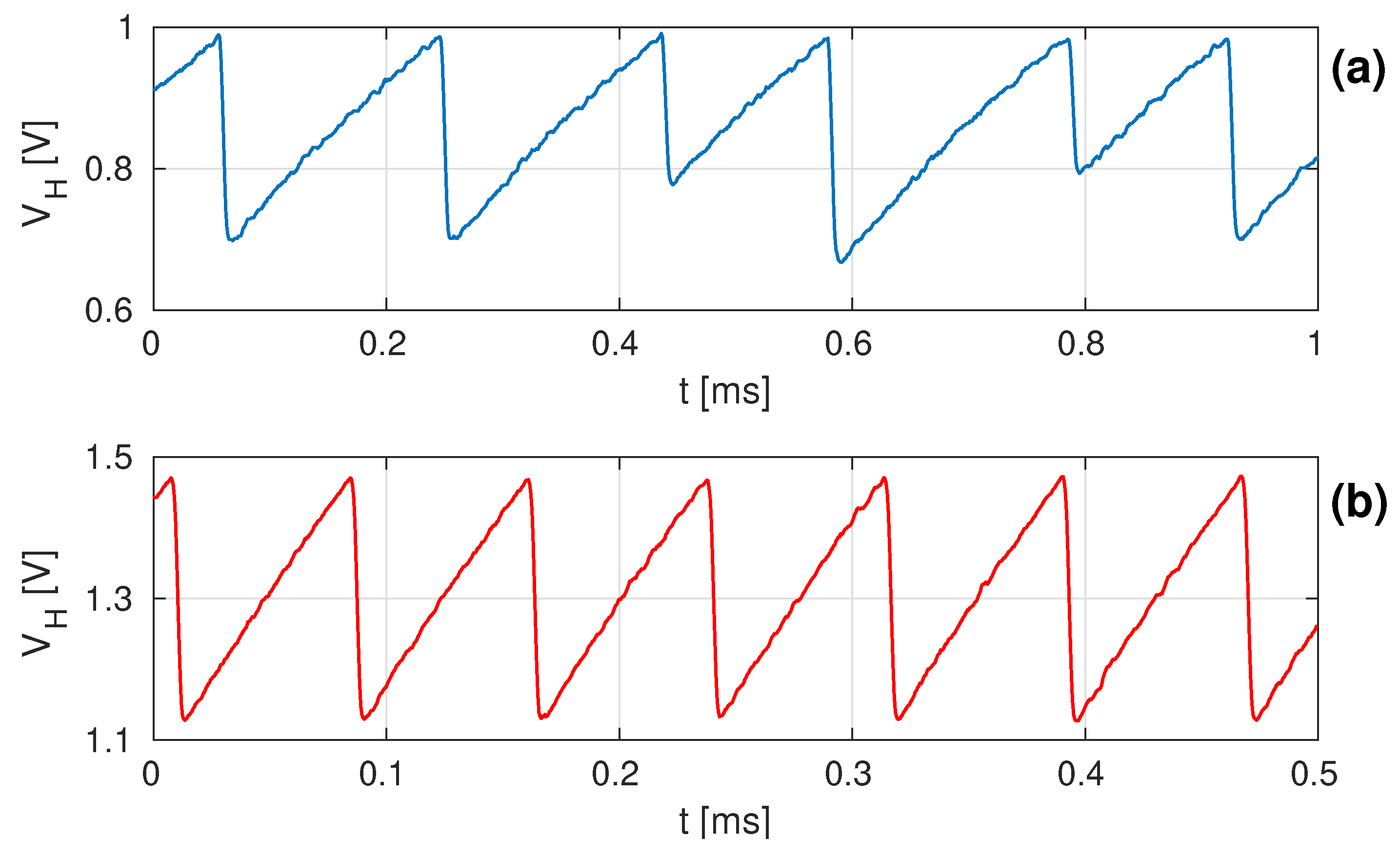
In order to characterize the DC-DC converter, the output voltage and current were, respectively, forced and measured by a Keithley Source and Measurement Unit (SMU) [24]. A linear power supply generator combined with a 500 k series resistor replaced the RF rectifier and was used to supply the converter. The value of the resistor was upper limited by the maximum output voltage of the supply generator, and it is close to the typical values of output resistance of RF rectifiers available in literature. The measured voltage waveforms at the DC-DC converter input in the case of = 1.3 V and = 2.0 V are shown in Figure 8a,b, respectively. The trace in Figure 8a was obtained with a low available input power, with an average output power equal to 310 nW, whereas the measurement of Figure 8b was carried out with a higher input power, corresponding to 2.9 W delivered power. It is worth noticing that, in the former case, the recharging phase of the intermediate reservoir is longer, due to the lower available input power, thus leading to a lower frequency of the signal in Figure 2. The average value of tracks the value of the main reservoir voltage, as required to fulfill condition (9).
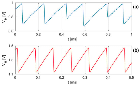
Figure 8.
Measured voltage waveforms at the DC-DC converter input. (a) = 1.3 V, = 310 nW; (b) = 2 V, = 2.9 W.
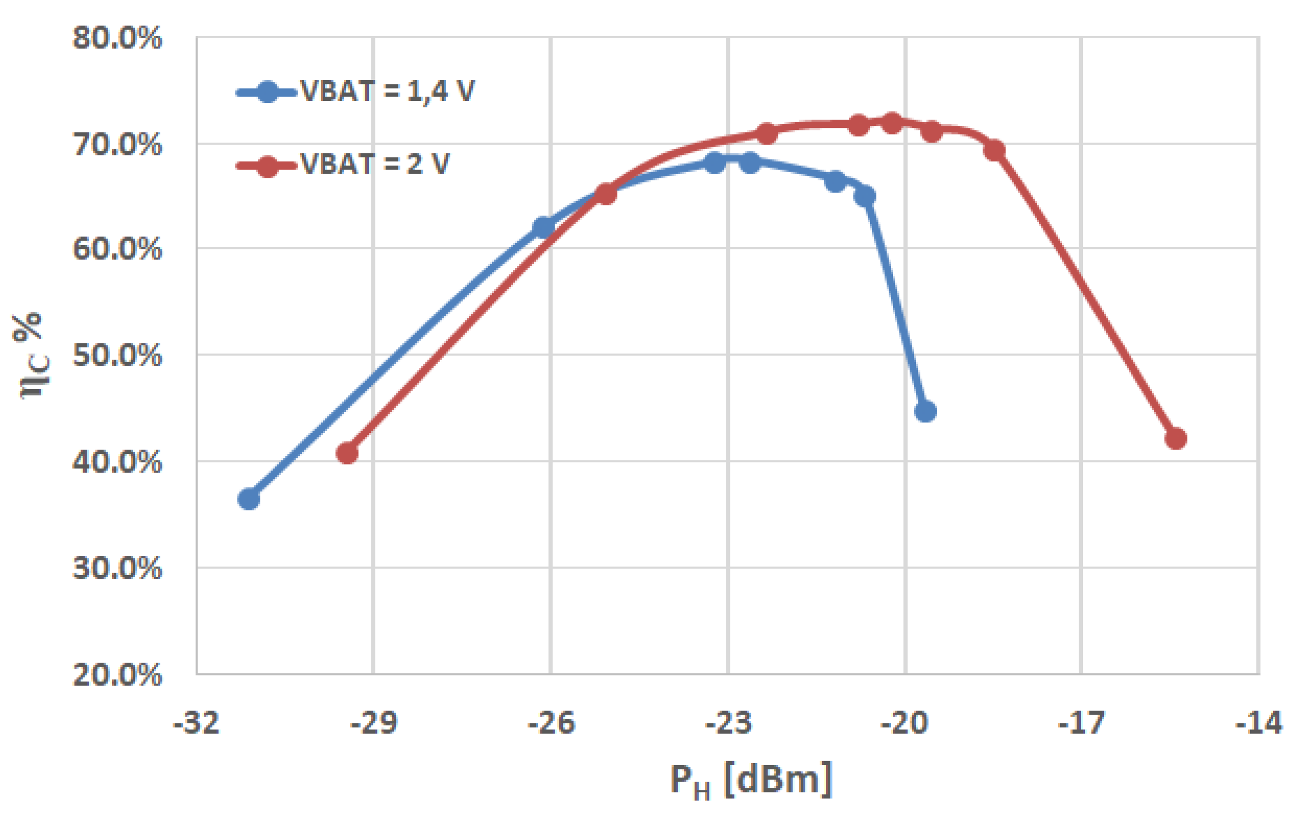
The measured efficiency of the DC-DC converter, is shown in the plot of Figure 9, in the cases of a main reservoir voltage of 1.4 V and 2 V. In both cases, vs. the input power exhibits an absolute maximum. Indeed, at low input power, the internal power consumption is dominated by the static contribution of the control circuit and by the circuit driving the MOS switches, and , whereas, at higher input power levels, the most relevant contributions are the series resistance of the switches in on-state and the series resistance of .

Figure 9.
Measured DC-DC converter efficiency vs. input power at = 1.2 V (blue line) and = 2 V (red line).
The simulated current consumption at 1.4 V of the monitor section , and of the clock-generator section are reported in Table 2 for the recharging and the energy-transfer phases.

Table 2.
Current consumption of the DC-DC converter blocks.
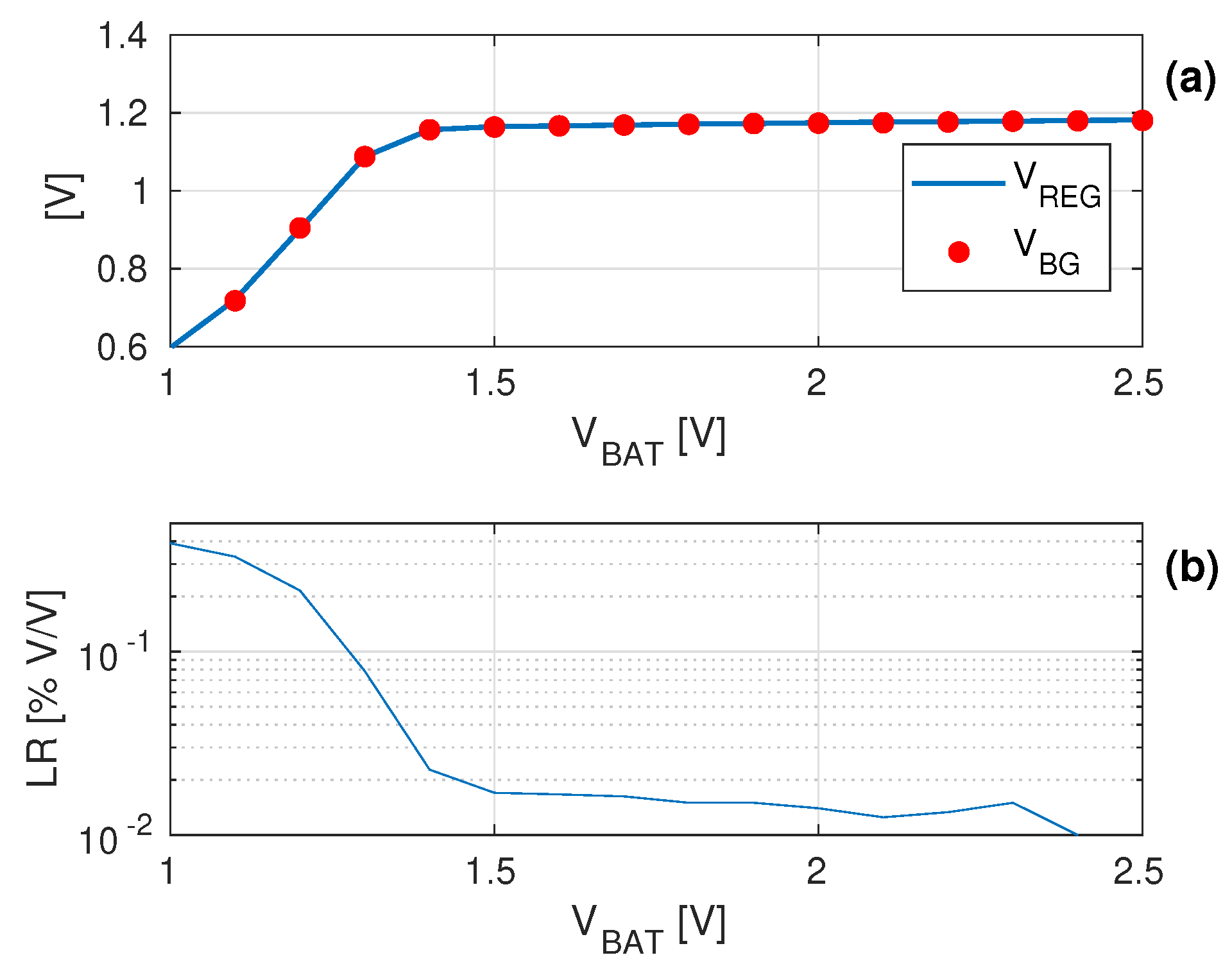
The LDO and the bandgap reference exhibit an overall current consumption of 4.7 A at the room temperature, with 1.9 A required by the LDO. The silicon area without capacitor is 25.5 m × 27.75 m. is implemented with a thin-oxide MOS device and exhibits a typical value of 1 nF. In order to characterize the bandgap reference and the LDO, both circuits were disconnected from the main reservoir and supplied by a programmable power supply generator. In Figure 10a, the LDO output and the reference voltage are measured over a large range of the unregulated supply . The test was carried out with a DC load current equal to 10 A. The measured load regulation LR is shown in Figure 10b, where and is the shift of the LDO output with respect to the case of = 2.5 V.
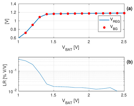
Figure 10.
(a) measured bandgap reference voltage (red circles), and regulated voltage (solid blue line) vs. . (b) LDO line regulation at = 2.5 V.
A low-power temperature sensor with a dedicated Analog-to-Digital converter (ADC) was integrated in the test chip [25]. Thus, the sensor with the power-management circuit and an RF rectifier compose the structure of an autonomous sensor node, as in Figure 1. The temperature sensor is based on a pair of p-n junctions with the same size and different bias currents. The sensor output, which is the difference of the bias voltage of the two p-n diodes, exhibits PTAT behavior. The conversion of the sensor output to the digital domain is performed by a Sigma-Delta ADC [25,26]. The digital filter is not integrated in the test chip. Thus, the decimation and filtering of the ADC serial output are performed off-chip. With an optimized digital filter, a nominal resolution higher than 10-b is obtained with an acquisition time of about 15 ms, corresponding to a temperature resolution lower than 0.1 °C over 100 °C of temperature range. The measured current consumption of the whole temperature sensing circuit composed by the sensor, the ADC, and the clock chain, is 4.5 A at room temperature.
The energy harvesting system in Figure 1, except the RF rectifier, was characterized together with the temperature sensor working in duty-cycle mode. Taking into account that the performance of the proposed power management does not depend on the RF rectifier topology used for the energy harvesting from the tuned antenna, the rectifier was replaced with an SMU [24] configured as a constant current generator and voltage meter. This test-setup allows for measuring the power efficiency of the power management block, including the DC-DC converter with input control, the off-chip charge reservoir, and the LDO. It is worth noticing that the DC-DC converter is always active if the reservoir voltage is higher than 1.1 V, whereas the LDO with the bandgap reference is enabled only during each temperature measurement phase. In order to limit the time span of the oscilloscope acquisition, the activation frequency of the sensor was set to 6.6 sample/s corresponding to a time lapse between two successive temperature measurements of 150 ms. This activation frequency is significantly higher than the typical values used in WSN applications, where is usually on the order of several seconds. The acquisition time of the ADC bit stream was set to 25 ms, thus higher than the minimum achievable value with an optimized digital filter. Therefore, this set-up corresponds to a worse case in terms of energy consumption, but to a simpler implementation of the digital filter, with a smaller silicon area. In the test, the data were acquired by an FPGA and processed by MATLAB scripts running on a laptop to obtain 12-b data for each temperature measurement.
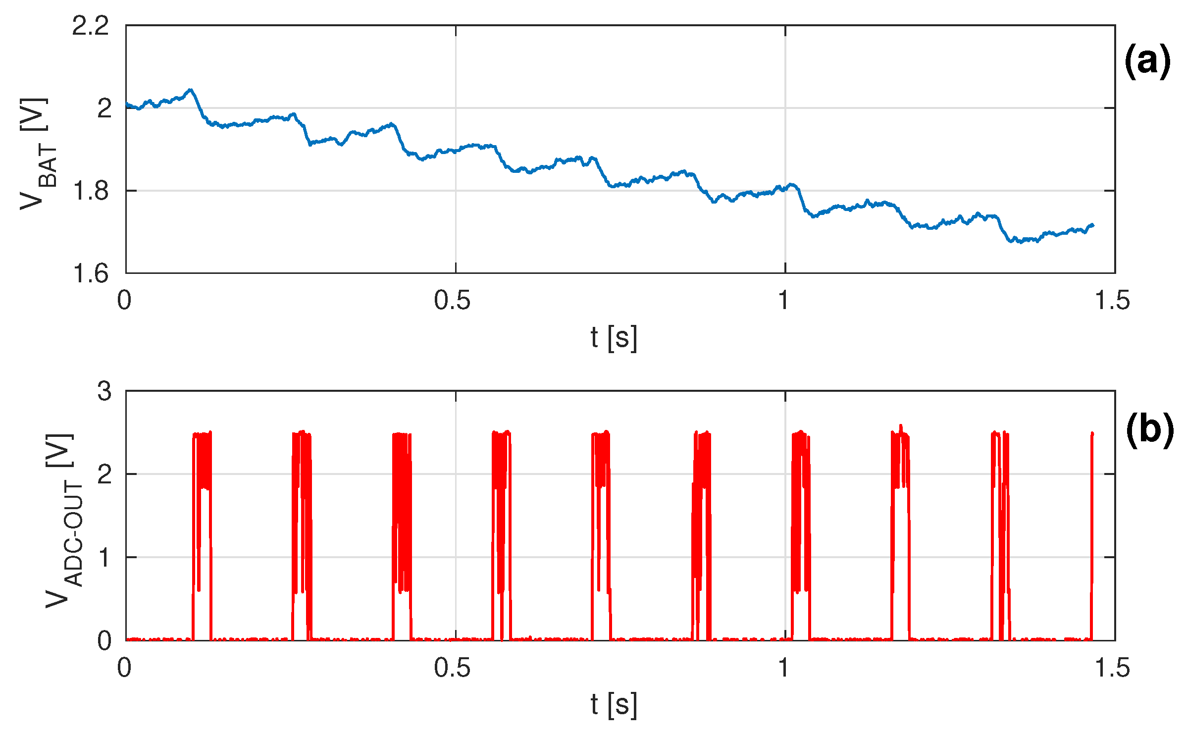
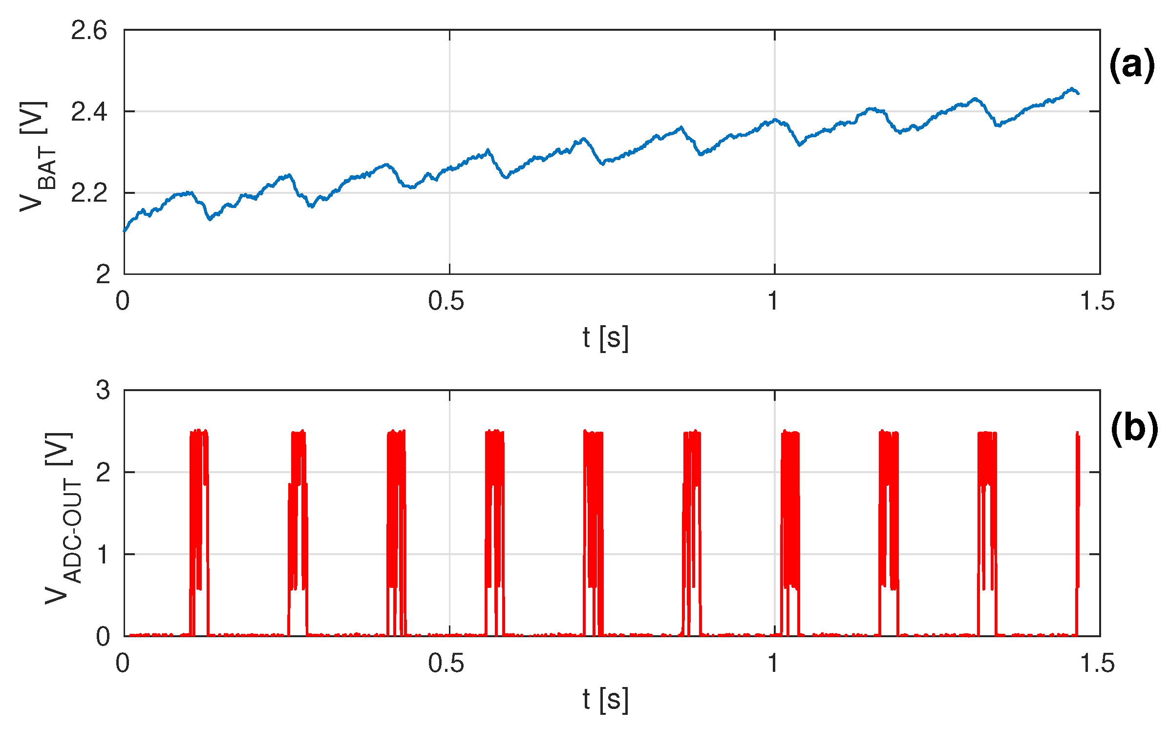
The oscilloscope traces in Figure 11 correspond to the voltage of the main reservoir (top graph, blue trace), and to the ADC serial output (bottom graph, red trace), with 6.9 A current supplied by the SMU to the DC-DC converter, with an average input voltage equal to 1.44 V. In the test, the charge reservoir was pre-charged to 2.1 V and the diode in Figure 1 replaced by a switch disconnecting the auxiliary battery before the oscilloscope acquisition. The ripple of the reservoir voltage is due to the activation of the sensing circuits and of the LDO, which require 135 nJ and 246 nJ, respectively, for each measurement. In this test, the energy supplied to the DC-DC converter leads to an average balanced condition on the amount of charge stored into the main reservoir. Therefore, this is the minimum energy required to supply the sensor with the LDO without draining a supplementary energy from an auxiliary battery. The measurement results in Figure 12 and Figure 13 are obtained with an average input power respectively lower and higher than the minimum value. In the former case, the reservoir voltage progressively decreases until the threshold voltage of 1.1 V is reached and the DC-DC converter is disabled, since the energy supplied to the converter is not enough to sustain the sensor with the LDO at the measurement rate of 6.6 Sample/s. On the contrary, in the measurement of Figure 13, the excess energy is stored in the reservoir.
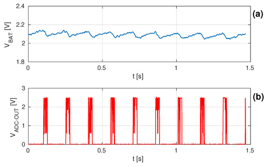
Figure 11.
Oscilloscope measurements of the system in Figure 1 with the rectifier replaced by a constant current generator = 6.9 A, the charge reservoir pre-charged at = 2.1 V, and the auxiliary battery disconnected. (a) trace; (b) ADC serial output.
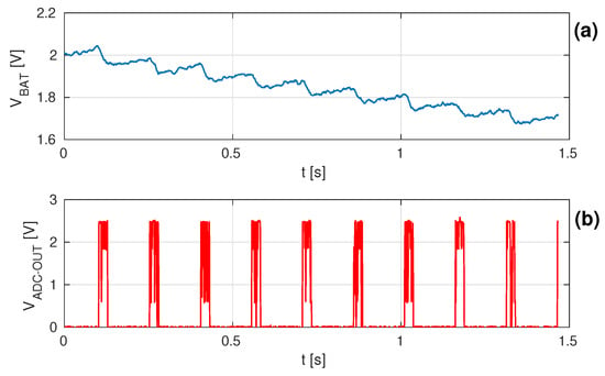
Figure 12.
Oscilloscope measurements with the same set-up of Figure 11. Input power lower than the minimum value to sustain the sensing circuits. (a) trace; (b) ADC serial output.
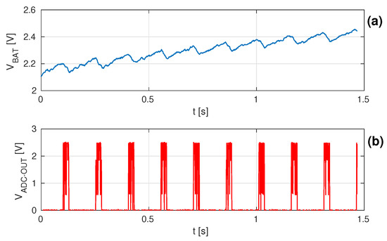
Figure 13.
Oscilloscope measurements with the same set-up of Figure 11. Input power higher than the minimum value to sustain the sensing circuits. (a) trace; (b) ADC serial output.
The efficiency of the whole power management system is calculated for the balanced condition in Figure 11, which requires 4.46 W at the DC-DC converter input. Considering the measured current consumption of the sensing circuit and of the LDO are 4.5 A at 1.2 V and 4.7 A at 2.1 V , respectively, with the sampling rate of 6.6 Sample/s an overall PMU efficiency of 20% is obtained.
Starting from the energy consumption of the internal blocks composing the power management, the minimum RF available power required to supply the sensor at lower measurement rates can be estimated. In the following analysis, a measurement rate of 1 Sample/s is assumed with an optimized ADC digital filter that allows for limiting the measurement time to 15 ms, thus leading to 80 nW of average power required by the sensing circuits. The efficiency of the LDO depends on the reservoir voltage and on the current consumption of the bandgap and the amplifier in Figure 6:
where is the internal current consumption of the LDO with the bandgap reference, and is the supply current of the temperature sensor with the ADC. It is worth noticing that, in the system of Figure 1, the sensor with the ADC and the LDO with the bandgap are activated by means of the enable signal with a programmed acquisition rate of 1 Sample/s. At the end of the measurement, all the blocks are driven in power down mode. Thus, the current consumption of the LDO and the bandgap must be averaged over the time interval between two successive measurements. Given a measurement rate of 1 Sample/s, = 4.7 A, = 4.5 A, and = 2 V, an LDO efficiency of approximately 30% is obtained, with 138 nA of average current supplied by the reservoir.
The measured efficiency of the DC-DC converter allows for computing the minimum power that must be delivered by the rectifier, i.e., = 395 nW. Finally, the RF power required to supply the sensor is affected by the efficiency of the RF rectifier. A typical range of 20–40% is found for the power efficiency of CMOS UHF rectifiers reported in literature [9,12]. Considering = 30%, a minimum RF power level of dBm is obtained. Given the matching of the antenna with the input impedance of the rectifier, this power value corresponds to the available RF power required at the antenna terminal to supply the sensor without draining energy from the auxiliary battery . The analytic expression of the minimum available power required to supply the sensor is obtained considering the power efficiency of the involved blocks and the reflected power at the RF input due to the residual impedance mismatch:
Thus, in case of impedance mismatch at the antenna–rectifier interface, the value of dBm must be increased accordingly to obtain the minimum available RF power. It is worth noticing that the RF power levels obtained in this analysis are available in both urban and semi-urban environment in the 900 MHz frequency bands actually allocated for the 4G and the 3G mobile phone services [8]. The results of the power budget calculation are summarized in Table 3.

Table 3.
Power budget of the power harvesting and management system.
Table 4 shows the maximum and average values in different urban environments and frequency bands [6,7,8,13].

Table 4.
RF available power in urban environments.
4. Conclusions
A power management system for the generation of the power supply of WSNs from RF energy harvesting has been presented. A DC-DC boost converter is used to recharge an energy reservoir, while a linear regulator scales down the output voltage for an integrated temperature sensor. The input driven DC-DC converter makes the power management inherently independent of the rectifier design, and it achieves in measurement a peak efficiency of 70%, with an input power of 395 nW. The measurement results of the fundamental blocks make the system suitable for the generation of the power supply of WSNs. Particularly, with an input RF power of dBm, the power management sustains a measurement rate of 1 Sample/s with a temperature sensor and an analog-to-digital converter.
Author Contributions
Conceptualization, formal analysis, validation, methodology, writing—original draft: M.C. and A.B.; resources, writing—review and editing: M.C., A.B., and M.R.; supervision: A.B. All authors have read and agreed to the published version of the manuscript.
Funding
This research received no external funding.
Acknowledgments
The authors are grateful to Elio Guidetti of STMicroelectronics for supporting this project. The support of STMicroelectronics for the silicon prototyping is acknowledged.
Conflicts of Interest
The authors declare no conflict of interest.
References
- Vullers, R.J.M.; Schaijk, R.V.; Visser, H.J.; Penders, J.; Hoof, C.V. Energy Harvesting for Autonomous Wireless Sensor Networks. IEEE Solid State Circuits Mag. 2010, 2, 29–38. [Google Scholar] [CrossRef]
- Bi, S.; Ho, C.K.; Zhang, R. Wireless powered communication: Opportunities and challenges. IEEE Commun. Mag. 2015, 53, 117–125. [Google Scholar] [CrossRef]
- Bi, S.; Zeng, Y.; Zhang, R. Wireless powered communication networks: An overview. IEEE Wirel. Commun. 2016, 23, 10–18. [Google Scholar] [CrossRef]
- Darsena, D.; Gelli, G.; Verde, F. Cloud-Aided Cognitive Ambient Backscatter Wireless Sensor Networks. IEEE Access 2019, 7, 57399–57414. [Google Scholar] [CrossRef]
- Lu, X.; Wang, P.; Niyato, D.; Kim, D.I.; Han, Z. Wireless Networks With RF Energy Harvesting: A Contemporary Survey. IEEE Commun. Surv. Tutor. 2015, 17, 757–789. [Google Scholar] [CrossRef]
- Rangel, M.P.; Mitcheson, P.D.; Lucyszyn, S. Ambient RF Energy Harvesting in Urban and Semi-Urban Environments. IEEE Trans. Microw. Theory Tech. 2013, 61, 2715–2726. [Google Scholar] [CrossRef]
- Muncuk, U.; Alemdar, K.; Sarode, J.D.; Chowdhury, K.R. Multi-band Ambient RF Energy Harvesting Circuit Design for Enabling Battery-less Sensors and IoTs. IEEE Internet Things J. 2018. [Google Scholar] [CrossRef]
- Caselli, M.; Tonelli, M.; Boni, A. Analysis and design of an integrated RF energy harvester for ultra low-power environments. Int. J. Circuit Theory Appl. 2019, 47, 1086–1104. [Google Scholar] [CrossRef]
- Nakamoto, H.; Yamazaki, D.; Yamamoto, T.; Kurata, H.; Yamada, S.; Mukaida, K.; Ninomiya, T.; Ohkawa, T.; Masui, S.; Gotoh, K. A Passive UHF RF Identification CMOS Tag IC Using Ferroelectric RAM in 0.35-μm Technology. IEEE J. Solid State Circuits 2007, 42, 101–110. [Google Scholar] [CrossRef]
- Rincon-Mora, G.A.; Allen, P.E. A low-voltage, low quiescent current, low drop-out regulator. IEEE J. Solid State Circuits 1998, 33, 36–44. [Google Scholar] [CrossRef]
- Caselli, M.; Boni, A. Modeling and design of 3D MPPT for ultra low power RF energy harvesters. Integration 2020, 72, 21–28. [Google Scholar] [CrossRef]
- Stoopman, M.; Keyrouz, S.; Visser, H.J.; Philips, K.; Serdijn, W.A. Co-Design of a CMOS Rectifier and Small Loop Antenna for Highly Sensitive RF Energy Harvesters. IEEE J. Solid State Circuits 2014, 49, 622–634. [Google Scholar] [CrossRef]
- Khemar, A.; Kacha, A.; Takhedmit, H.; Abib, G. Design and experiments of a dual-band rectenna for ambient RF energy harvesting in urban environments. IET Microw. Antennas Propag. 2018, 12, 49–55. [Google Scholar] [CrossRef]
- Facen, A.; Boni, A. CMOS power retriever for UHF RFID tags. Electron. Lett. 2007, 43, 1424–1425. [Google Scholar] [CrossRef]
- Papotto, G.; Carrara, F.; Palmisano, G. A 90-nm CMOS Threshold-Compensated RF Energy Harvester. IEEE J. Solid State Circuits 2011, 46, 1985–1997. [Google Scholar] [CrossRef]
- Seigneuret, G.; Bergeret, E.; Pannier, P. Auto-tuning in passive UHF RFID tags. In Proceedings of the 8th IEEE International NEWCAS Conference, Montreal, QC, Canada, 20–23 June 2010; pp. 181–184. [Google Scholar] [CrossRef]
- Liu, Z.; Hsu, Y.; Hella, M.M. An RF powering system with adaptive impedance matching for individual health monitoring applications. In Proceedings of the 2016 38th Annual International Conference of the IEEE Engineering in Medicine and Biology Society (EMBC), Orlando, FL, USA, 16–20 August 2016; pp. 4983–4986. [Google Scholar] [CrossRef]
- Bergeret, E.; Gaubert, J.; Pannier, P.; Gaultier, J.M. Modeling and Design of CMOS UHF Voltage Multiplier for RFID in an EEPROM Compatible Process. IEEE Trans. Circuits Syst. II Express Briefs 2007, 54, 833–837. [Google Scholar] [CrossRef]
- Umeda, T.; Yoshida, H.; Sekine, S.; Fujita, Y.; Suzuki, T.; Otaka, S. A 950-MHz rectifier circuit for sensor network tags with 10-m distance. IEEE J. Solid State Circuits 2006, 41, 35–41. [Google Scholar] [CrossRef]
- C2M1CXS-053 Murata Supercapacitor Technical Note. Murata Manufactoring Co. Available online: https://www.murata.com/~/media/webrenewal/products/capacitor/edlc/techguide/electrical/c2m1cxs-053.ashx (accessed on 18 September 2020).
- Application Notes for Multilayer Ceramic Capacitors. Kemet Co. Available online: https://content.kemet.com/datasheets/F3101_CerMoldAxRad.pdf (accessed on 18 September 2020).
- Schillinger, D.; Hu, Y.; Amayreh, M.; Moranz, C.; Manoli, Y. A 96.7% efficient boost converter with a stand-by current of 420 nA for energy harvesting applications. In Proceedings of the 2016 IEEE International Symposium on Circuits and Systems (ISCAS), Montreal, QC, Canada, 22–25 May 2016; pp. 654–657. [Google Scholar] [CrossRef]
- SDR0503 Series-SMD Power Inductors. Bourns. Available online: https://www.bourns.com/docs/product-datasheets/sdr0503.pdf?sfvrsn=12b87159_15 (accessed on 18 September 2020).
- Model 2400 Series SourceMeter User’s Manual; 2400s-900-01 Rev. K; Keithley Instruments, Inc.: Cleveland, OH, USA, 2011.
- Garulli, N.; Boni, A.; Caselli, M.; Magnanini, A.; Tonelli, M. A low power temperature sensor for IOT applications in CMOS 65nm technology. In Proceedings of the 2017 IEEE 7th International Conference on Consumer Electronics-Berlin (ICCE-Berlin), Berlin, Germany, 3–6 September 2017; pp. 92–96. [Google Scholar] [CrossRef]
- Pertijs, M.A.P.; Makinwa, K.A.A.; Huijsing, J.H. A CMOS smart temperature sensor with a 3σ inaccuracy of 0.1 °C from −55 °C to 125 °C. IEEE J. Solid State Circuits 2005, 40, 2805–2815. [Google Scholar] [CrossRef]
© 2020 by the authors. Licensee MDPI, Basel, Switzerland. This article is an open access article distributed under the terms and conditions of the Creative Commons Attribution (CC BY) license (http://creativecommons.org/licenses/by/4.0/).

