Abstract
The suppression of residual reflectivity in optical elements has become a hot research topic as it addresses the degradation of optical system imaging quality caused by stray light. Antireflective coatings on the outer surface of window glasses require low reflectivity, high hardness, and resistance to mechanical wear. This study investigates the role of reactive gas stoichiometry in tailoring the structure and performance of antireflection (AR) coatings deposited on GG7i glass via capacitively coupled radio-frequency magnetron sputtering. First, the influence of three / flow ratios on the optical and mechanical properties of films discussed under identical process parameters. Results show that the refractive index, hardness, and surface roughness of the films increase with increasing / ratio and that the stress of the films increases according to the Stoney formula. The wear resistance of the films combined with an antifingerprint (AF) coating is tested using steel wool. Experimental results show that the water contact angle of the AF decreases with increasing surface roughness of the film. Finally, on the basis of a comprehensive evaluation of optical and mechanical properties, the antireflection coating on the outer surface of the window glass was prepared by optimizing the process parameters. At incidence, the average reflectivity from 420 to 680 nm is <1%, the maximum value is <1.2%, the surface hardness is 17.2 GPa, and the water contact angle is after the steel wool wear test, showing its suitability for durable antifingerprint applications. This work provides a strategic pathway for designing high-performance optical coatings with tailored mechanical robustness.
1. Introduction
With the continuous evolution of photoelectric imaging systems, better antireflection performance is required from optical elements [1,2,3,4]. Thus, reducing reflectivity to eliminate ghost effects has become a key issue and research hotspot in this field. Hard antireflection (AR) coatings are generally applied to the outer surface of protective glass in optical systems. Deposition of such coatings effectively reduces residual reflection and enhances the surface hardness of the protective glasses. Materials used for preparing hard AR coatings are , , boron nitride, and silicon oxynitride. Of these, silicon oxynitride () is an optical thin-film material known for its tunable refractive index, ultra-low absorption, high hardness, and excellent adhesion to glass substrates. The primary mainstream methods for preparing silicon oxynitride thin films are magnetron sputtering deposition, plasma-enhanced chemical vapor deposition (PECVD), and atomic layer deposition (ALD). PECVD-prepared silicon oxynitride films are primarily used in the semiconductor field. Precursor gases are typically generally a mixture of silane (), nitrogen (), and , with a deposition temperature generally ranging from 300 °C to 500 °C. This process inevitably introduces hydrogen (from and ) into the film in the form of Si–H and N–H bonds. A high hydrogen content interrupts the dense Si–O–N network, resulting in a loose film structure and marked reduction in hardness and corrosion resistance [5,6]. For the ALD of silicon oxynitride films, chlorosilane () is used as the silicon precursor, as the oxygen source, and as the nitrogen source (thermal nitridation and temperature of >400 °C). The primary advantage of is its ability to grow on substrates with complex shapes while maintaining excellent thickness uniformity. However, the growth rate is slow and high-temperature film formation is required, making it less advantageous for mass production of large-sized substrates [7].
The preparation of silicon oxynitride films via magnetron sputtering primarily utilizes inductively coupled (ICP) or capacitively coupled (CCP) to ionize nitrogen and oxygen ions [8]. These ions combine with Si atoms ejected from the target via argon-ion bombardment to form films. This method features a low film formation temperature and is conducive to mass production. Several studies have been conducted on the preparation of hard AR coatings via magnetron sputtering. For instance, Price et al. prepared antireflection coatings via reactive magnetron sputtering of silicon dioxide and silicon oxynitride and they reported that increasing the thickness of silicon oxynitride in the intermediate layer helps improve film wear resistance [9]; Özhan, A.E.S. et al. prepared hard antireflection coatings via radio-frequency (RF) magnetron sputtering of boron nitride and boron carbide and achieved a single-sided transmittance of 94% over 3600–4900 nm and a hardness of 9.13 GPa [10]; Fu, X. et al. employed magnetron sputtering to deposit aluminum oxynitride and silicon nitride and reported an average hardness of 1773.9 Hv and an average visible-band reflectivity of 0.489% [11]; Law, A.M. et al. prepared antireflection films on glass substrates via RF magnetron sputtering of zirconium oxide and silicon dioxide and achieved an average reflectivity of 1.71% over 350–1150 nm [12].
From the aforementioned references, the refractive index of films can be tuned by adjusting the ratio of / [13]. However, several problems persist regarding magnetron -sputtered silicon oxynitride, such as low absorption of , the influence mechanism of process parameters on the surface morphology of the film, crystal structure, and chemical bonds required to be studied to obtain high hardness. Several reports exist on the optical constants, hardness, roughness of , and the wear resistance of the combination of antifingerprint (AF) coatings with hard AR coatings.
This study employs CCP magnetron sputtering to prepare silicon oxynitride films. Under the same process parameters, the growth mechanism of composite films exhibiting different / ratios was studied. The optical constants within the visible light band were calculated, and the optical properties, structure, and mechanical properties were examined. Steel wool testing was conducted to evaluate the wear resistance of the combination of hard AR coatings exhibiting AF coatings. Finally, based on a comprehensive assessment of optical and mechanical properties, the preparation of AR coatings for the outer surface of window glass was completed.
2. Materials and Methods
2.1. Sample Preparation
films were prepared using a Bühler Leybold 2050 magnetron sputtering machine (Bullerwinkel Optoelectronics Equipment (Beijing) Co., Ltd., Beijing, China) (Figure 1a). The target was placed 5 cm away from the substrate, deposition temperature < 120 °C.
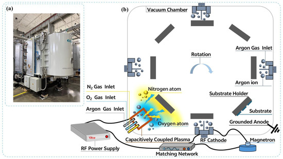
Figure 1.
Principle of capacitively coupled magnetron sputtering equipment and fabrication of silicon oxynitride films. (a) Capacitively coupled magnetron sputtering equipment. (b) Principle of silicon oxynitride film fabrication.
The purity of the silicon target was 99.99%, the relative density was >99%, and the grain size was <100 μm. CCP argon-ion cleaning was performed for 30 min before each coating to ensure complete removal of the oxide layer and impurities on the surface of the silicon target, which is referred to as “target cleaning”. TA glass with good plasticity was used as a substrate; it exhibited a diameter of 10 mm and a thickness of 0.5 mm. Figure 1b illustrates the fabrication of silicon oxynitride () films via CCP magnetron sputtering: First, nitrogen, oxygen, and argon gases were introduced into a CCP plasma device at a specific ratio to generate a plasma state, thereby generating nitrogen and oxygen atoms. Subsequently, argon gas was introduced at the target position and ionized using a RF source to generate argon ions. Mutually perpendicular electric and magnetic fields were distributed within the silicon target. Under the influence of Lorentz force, the argon ions bombard the target, ejecting silicon atoms. Finally, the sputtered silicon atoms combined with the oxygen and nitrogen atoms generated via capacitive coupling to form silicon oxynitride, which deposited onto the substrate and subsequently formed a silicon oxynitride thin film via diffusion and migration. First, a polishing solution with a particle size of 1.5 μm was used for rough polishing, followed by a polishing solution with a particle size of 0.8–1 μm for medium polishing, and finally a polishing solution with a particle size of 0.35 μm for fine polishing. The influence of surface roughness [14,15], surface type, and substrate scattering on film characterization was eliminated, and the root-mean-squared roughness of the substrate was ultimately reduced to 0.007 μm. GG7i glass (Corning Display Technologies (Hefei) Co., Ltd., Hefei, China)—polished on both sides—was used as the substrate. The initial vacuum level of the magnetron sputtering chamber was set to Pa, and the / flow ratios were 230:230, 430:200, and 430:120 sccm. The capacitively coupled power was 6 kW, and the target power and deposition time were set to 10 kW and 1500 s, respectively. The AF coating was deposited via resistance heating evaporation, and its main component was perfluoropolyether (PFPE) [16]. The conditions for the steel wool wear resistance test were as follows: temperature = 16–28 °C, humidity of ≤50%RH, stroke length = 20 mm, with 8000 operations (4000 cycles) and 500-g load.
2.2. Characterization of Films
The transmittance and reflectance of the thin films were measured using an Agilent Cary 7000 spectrophotometer (Agilent Technologies (China) Co., Ltd., Shanghai, China) with a wavelength step of 1 nm and a resolution of 2 nm. The optical constants were fitted using the Macleod software. The chemical composition ratio and chemical bond characteristics of the films films were measured via X-ray photoelectron spectroscopy (XPS). The X-ray electron energy was 1486.6 eV, and the energy step size was 0.2 eV. The structure of the films was investigated using a Shimadzu XRD-6000 (X-ray diffractometer) (Shimadzu Corporation (China) Co., Ltd., Shanghai, China) with copper target radiation of wavelength 1.5406 Å, and the binding energy of contaminated carbon (C1s 284.8 eV) was used as the reference.
The hardness of the films was measured using a nanoindenter employing the continuous stiffness measurement technique [17]. To ensure experimental accuracy and eliminate randomness, each sample was measured thrice under consistent processing parameters (target power, film thickness, and deposition rate) and the average value was calculated. These three data points were obtained from different coating areas within the same batch. The testing conditions were as follows: diamond indenter, loading force = 10 mN, loading time = 10 s, and loading rate = 0.5 mN/s. The surface deformation and RMS roughness of the films were measured using a Zygo interferometer (ZYGO, Middlefield, CT, USA). The stress of the films was analyzed using the Stoney formula. The elastic modulus, hardness, and roughness of the thin films were obtained by performing the above-mentioned tests. The relationship between films and the AF coating combined with steel wool wear resistance was analyzed.
3. Experimental Results and Discussion
3.1. Visible Optical Properties of Films
Envelope method is an optical technique used for determining refractive index (n), extinction coefficient (k), and thickness (d) of thin films by analyzing the extrema (maxima and minima) in the transmittance spectrum of the film [18]. First, the intermediate variable N is calculated using the transmittance minima and Equation (1), which corresponds to the half-wavelength interference condition of the film. Under this condition, the optical path difference is primarily determined by the geometric thickness. Given the refractive index of the glass substrate (), the refractive index (n) of the film can be derived from Equation (2). Subsequently, the physical thickness d can be calculated using Equation (5), based on the wavelength positions ( and ) of the interference extrema. Here, m represents the interference order (an integer) and and denote the refractive indices at their respective wavelengths. Equation (5) helps calculating the thickness using the optical path difference between adjacent extrema and is suitable for weakly absorbing films. Finally, by substituting the physical thickness d into Equation (3), the absorption coefficient is calculated using the transmittance maxima (), from which the extinction coefficient k is further derived. The above procedure was performed using the Macleod software. To enhance calculation accuracy, more extrema points were selected within the wavelength range of 400–1100 nm [19,20].
Figure 2a illustrates the reflectance and transmittance curves of single-layer films. Figure 2b presents the reflectance and transmittance of the GG7i glass substrate at a nitrogen and oxygen flow rate ratio of 430:120 sccm. It is known that the refractive index of films is higher than that of silicon dioxide [21]. From the reflectance curve, it can be concluded that peaks appear at even times of optical thickness. In other words, interference and cancellation occur with glass. Similarly, troughs appear at even times of optical thickness. The refractive index of films is fitted using the envelope method with the aid of Macleod film system design [22,23].
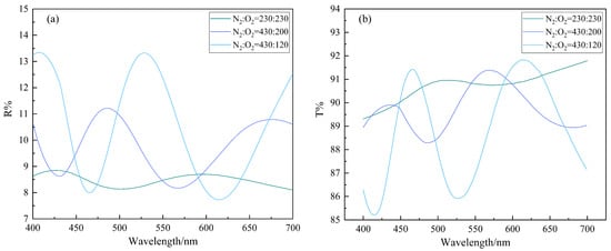
Figure 2.
Reflectance and transmittance of three / filled films: (a) Reflectance of films. (b) Transmittance of films.
The refractive index at a wavelength of 550 nm is 1.82, the extinction coefficient is essentially zero, and the monolayer film thickness is 497 nm, which is consistent with the thickness measured via ellipsometry (Figure 3). The thickness of the magnetron-sputtered film in this study is controlled by time. The thickness obtained from the first fitting was 497.6 nm, indicating a sputtering rate of 0.2488 nm/s. The coating time was set to 2000 s for repeatability verification. The fitted film thickness was 497.3 nm, which was in good agreement with the theoretical value. Figure 4 presents the refractive index and extinction coefficient of the three films exhibiting different / ratios. As / ratio decreases, the refractive index (n) increases monotonically and the extinction coefficient (k) decreases monotonically. On the basis of the density and dielectric constant analyses, the density of (2.2 g/) is lower than that of (3.1 g/), and the refractive index of the films lies between these two values. A decrease in oxygen content makes the film structure similar to that of dense , increases the dielectric constant, thereby increasing the refractive index and reducing the k value [24,25,26].
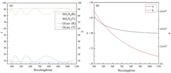
Figure 3.
Transmittance and reflectance curves and optical constants of films film with n = 1.82: (a) Reflectance and transmittance. (b) Refractive index and extinction coefficient.
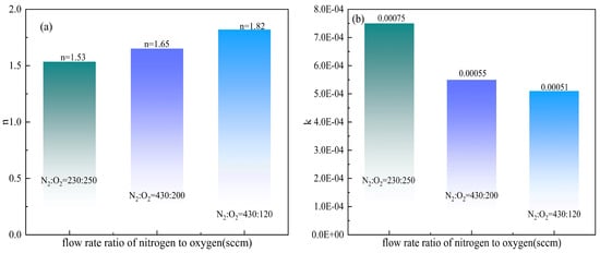
Figure 4.
Refractive indices and extinction coefficients of three films xhibiting different refractive indices: (a) Refractive Index and (b) extinction coefficient.
3.2. Structural Properties of Films
From the EDS results, it becomes evident that the proportion of nitrogen atoms increases and the content of oxygen atoms decreases, which is consistent with the trend in elemental composition expected from the experimental conditions (Table 1 and Figure 5). The Si–N bond (bond energy = 435 kJ/mol) forms a more highly cross-linked network than the Si–O bond (≈452 kJ/mol) [27]. Thus, the film exhibits a higher packing density, which reduces voids and gaps in the structure and increases the overall aggregation density of the film layer [22,28]. Consequently, the refractive index of gradually increases. The hardness of the films was measured using a nanoindentation tester. The elastic modulus increases with the refractive index, and the nanoindentation hardness increases as well (Figure 6). At a refractive index of 1.83, the film exhibits the highest nanoindentation hardness of 12.34 GPa and an elastic modulus of 85.84 GPa.

Table 1.
The chemical composition ratio of the film obtained by EDS measurement.
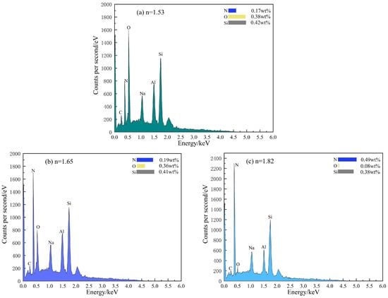
Figure 5.
EDS photoelectron spectroscopy of films film: (a) n = 1.53, (b) n = 1.65, and (c) n = 1.82.
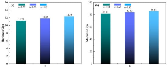
Figure 6.
Nanoindentation hardness of films with different refractive indices: (a) Hardness. (b) elastic modulus.
XPS is an effective method for obtaining quantitative information regarding film composition and chemical bonding [29,30,31,32]. Electronic correction was performed using the Advantage software. The binding energy of the C–C bond is 284.8 eV. Herein, peak fitting was applied to the N , Si and O spectra by adding 0.78 eV. Results obtained are presented in Figure 7. The refractive index of is 1.53 (Figure 7a). The N peak primarily consists of Si–O–N and Si–N bonds [33,34]. The bonding is relatively complex, and the noise level is high owing to the low nitrogen content, making data collection difficult. As the / flow ratio gradually increases, the bound electron cloud becomes weaker and more easily polarized and displaced by the optical field because the electronegativity of O (3.44) is stronger than that of N (3.04) [35,36]. A higher nitrogen content is associated with more easily polarizable electron clouds in the material, resulting in a higher refractive index, approaching the N binding energy of (typically 397.0–398.0 eV), which is consistent with the findings of Wu, C.Y. et al. [37]. Secondary peaks are observed in the N binding-energy region, indicating the presence of N–O bonds (Figure 7a,d,g). As the nitrogen flow increases from 230 to 430 sccm, the Si binding energy decreases (Figure 7g–i), corresponding to a higher nitrogen content. At a refractive index of 1.82, the Si binding energy becomes 102.36 eV. This is because, on average, the Si atoms exhibit additional low-electronegativity N neighbors and fewer high-electronegativity O neighbors. A higher electron cloud density produces a stronger shielding effect on the nucleus, making the removal of inner electrons easier, leading to a decrease in binding energy. Similarly, Figure 7g–i show that with a gradual increase in the / flow ratio, the O sliding energy decreases from 532.01 to 532.00 eV and then increases to 532.61 eV, with only slight variation. As the electronegativity of N is lower than that of O, the ability of the Si–N unit to withdraw electrons from the Si atom is weaker than that of the Si–O unit. The bonding electron cloud between O and Si becomes more biased toward the O atom to compete for electrons, decreasing the electron cloud density to O and slightly increasing its binding energy. In summary, when the refractive index of the film becomes 1.53, the N main peak appears at 399.82 eV. When n becomes 1.65, the N main peak appears at 397.80 eV. When nbecomes 1.82, the N main peak appears at 398.22 eV. The O binding energy changes only slightly, and the Si binding energy gradually decreases. XRD tests of the films with the three refractive indices show no diffraction peaks and show only morphous halos (Figure 7j–l). This indicates that the films with all three refractive indices exhibit amorphous growth structures [38,39], which corroborates the refractive-index and extinction-coefficient trends depicted in Figure 4.
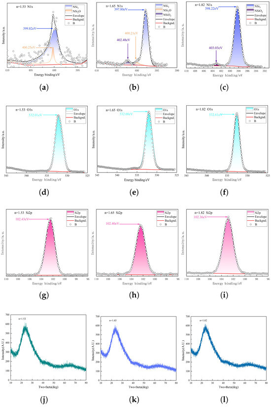
Figure 7.
XPS and XRD patterns of the films: (a) n = 1.53 N , (b) n = 1.65 N , (c) n = 1.82 N , (d) n = 1.53 O , (e) n = 1.65 O , (f) n = 1.82 O , (g) n = 1.53 Si , (h) n = 1.65 Si , (i) n = 1.82 Si , (j) n = 1.53, (k) n = 1.65, (l) n = 1.82.
3.3. Characteristics of Film Bonded with AF
When a film is deposited on the glass surface, it is subjected to a certain degree of strain. On the basis of the forces acting on the film on the substrate, the stress can be divided into tensile stress and compressive stress (Figure 8). Tensile stress occurs when the film is forced to extend outward, resulting in inward compression of the substrate, such that the film appears concave in the macro view; on the contrary, compressive stress makes the film appear convex in the macro view. The stress of the films primarily originates from thermal and internal stress. Thermal stress is primarily caused by the mismatch of thermal expansion coefficients between the glass substrate and films. The internal stress primarily depends on the microstructure and film density of SiO undefined N undefined thin films [40,41,42].
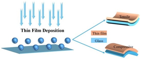
Figure 8.
Schematic diagram of the stress direction of the film.
The Stoney formula can be used to analyze the stress of the film layer [43,44,45]. First, the peak-to-valley value measured using a white light interferometer can reflect the bending height of the glass substrate (i.e., the vertical distance between the peak and the valley). Assuming that the glass substrate is almost spherically curved, the following equation can be obtained:
where denotes the layer stress (positive value indicates tensile stress and negative value indicates compressive stress), denotes the elastic modulus of the substrate ( = 64 GPa), denotes the Poisson ratio of the substrate ( = 0.2), and denote the substrate thickness and film thickness respectively, and and R denote the curvature radii before and after coating, respectively. The PV value becomes inversely proportional to the curvature radius R after coating. It can be observed from the Stoney formula that under a certain substrate material, the curvature radius after coating is inversely proportional to the film stress, that is, the larger the PV value, the larger the film stress . It can be concluded that as the refractive index of the thin film increases, the stress of the film layer increases. From the Zygo test results presented in Figure 9, it is evident that the root-mean-squared roughness increases with the refractive index.
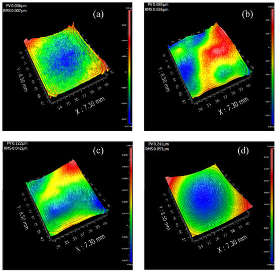
Figure 9.
Refractive index and surface roughness of the glass substrate and three types of films were measured using a Zygo interferometer. (a) Glass substrate, (b) n = 1.53 (c) n = 1.65 (d) n = 1.82.
Steel wool abrasion testing was used to measure the water contact angle of films with three refractive indices. The initial Water Contact Angle is between 113° and 115°. The water contact angle after steel wool abrasion test is present in Figure 10, verification was performed. The experiment was repeated three times, and the average value was recorded. Five different areas were measured in each set to calculate the average. From Figure 11, it can be observed that as surface roughness increases, the water contact angle decreases after steel wool wear testing. The Greenwood–Williamson micro-convex statistical model can be used to analyze the micro-stress distribution and predict the initial wear behavior when the physical vapor deposition coating contacts steel wool. The formulas and parameters are as follows [46]:
where W denotes the total normal load; Ar denotes the contact area, denotes the surface roughness (such as the Ra value of the coating), R denotes the curvature radius of the steel wool fiber, and denotes the equivalent elastic modulus when the film is in contact with steel wool. combines the elastic moduli E and of the two materials (unit: GPa). The Poisson ratios and are dimensionless, with typical values of 0.2–0.3. It describes the overall elastic response of the contact area. The calculation formula is as follows [47]:
thin-film coatings (E( = 1.53) = 11.21 GPa; E( = 1.65) = 11.82 GPa; E( = 1.82) = 12.34 GPa) and stainless steel wool ( = 19.3 GPa, = 0.3) were substituted into Equation (8) to obtain for the three films. Finally, substituting them into Equation (7) yields: (n = 1.53) ≈ 0.0108 GPa, (n = 1.65) ≈ 0.0111 GPa, (n = 1.82) ≈ 0.0113 GPa. According to Equation (7), under constant W and R, when the RMS roughness increases and the equivalent elastic modulus increases, the contact area Ar decreases. On the basis of the wear resistance mechanism, hydrophobicity hinders the formation of a lubricating film, resulting in stress concentration. The wear resistance of the film worsens [48,49]. The bonding mechanism between the AF and the coating indicates that siloxane hydrolyzes with water in the atmosphere to generate silanol groups (Figure 12) adhering the AF film to the glass substrate. The Si–O bond between AF and the coating is partially destroyed [50,51]. The RMS surface roughness was 0.316 mm before conducting the steel wool abrasion test, which increased to 0.952 mm after the test, indicating that the AF layer on the glass substrate surface had been damaged, and the water contact angle decreased.
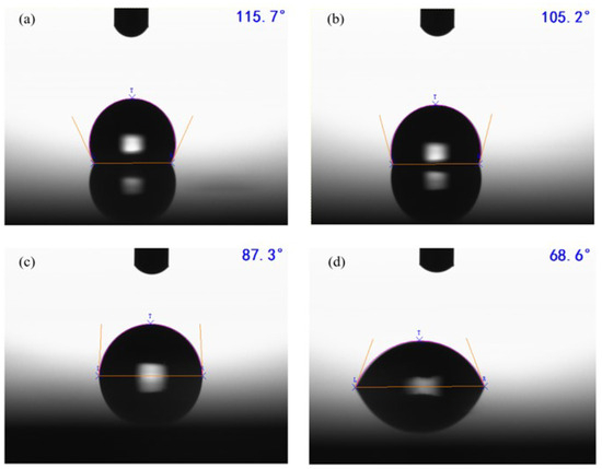
Figure 10.
Contact angle measurement: (a) Water contact angles of films with three refractive indices before testing, (b) Water contact angle after testing for n = 1.53, (c) Water contact angle after testing for n = 1.65, (d) Water contact angle after testing for n = 1.82.
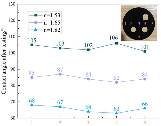
Figure 11.
Schematic diagram of the stress direction of the film.
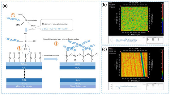
Figure 12.
Schematic illustration of the bonding mechanism between AF and the coating, and surface roughness after steel wool abrasion testing. (a) Schematic illustration of the interfacial bonding mechanism of AF and coating. (b) Before steel wool abrasion. (c) After steel wool abrasion.
The film was deposited onto a GG7i glass substrate to examine its application in optical imaging systems. On the GG7i glass substrate composite film (diameter: 45 mm, thickness: 0.68 mm) was deposited. The process parameters are listed in Table 2. The design of the antireflective film was completed using the Macleod thin-film design software. The initial structure was 0.14 . The design was optimized using the simplex algorithm and needle synthesis methods. As the optimized design produced extremely thin layers, complicating film fabrication, these thin layers were fixed and set to 10 nm to reduce manufacturing difficulty. The physical thickness and refractive index of the film layer are presented in Figure 13a. Figure 13b presents that the average reflectance is <1% and the maximum value is <1.5%.
Table 2.
Process Parameters.
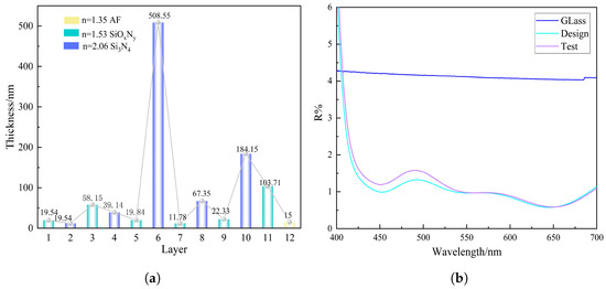
Figure 13.
Thickness and reflectivity of multilayer antireflective Coatings: (a) Physical thickness and refractive index of the hard antireflective film. (b) Spectrum of the hard antireflective film.
The nanoindentation hardness before coating was 7.3 GPa, which represents the surface hardness of glass (Figure 14b). The nanoindentation hardness after coating became 17.2 GPa (Figure 14d). By preparing the hard antireflection film, the hardness of the glass substrate increased by 8.9 GPa.
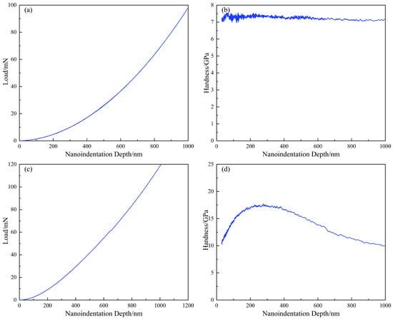
Figure 14.
Hardness and indentation depth of the glass substrate before and after coating in the 12-nm indentation test. (a) Load and depth before coating. (b) Hardness and depth before coating. (c) Load and depth after coating. (d) Hardness and depth after coating.
4. Conclusions
Amorphous films with three refractive indices were prepared via reactive magnetron sputtering. The relations between the films with three refractive indices and their surface, structure, morphology, and composition properties were investigated. As the / ratio increased, the refractive index, elastic modulus, and nanoindentation hardness of films increased. XPS analysis revealed that the number of Si peaks decreased as the refractive index of the film increased, indicating the presence of different bonds in the chemical composition of the film, and the chemical environment gradually became uniform. The Si–N bond (398.22 eV) was predominant, and the Si–O bond (403.03 eV) was secondary. The binding energy of O showed no obvious change but that of Si gradually decreased. Zygo images showed that the roughness of the film increases with the refractive index. Using the water contact angle after the steel wool wear evaluation test, the results showed that the higher the roughness, the lower the water contact angle of the film. The aforementioned experimental results revealed the inter-relationship between the refractive index, hardness, roughness, and reflectivity in film materials for antireflection coating design. The hard antireflective coating prepared in this study fulfills the optical requirement of an average reflectance of <1% within the visible wavelength range of 420–680 nm. Mechanically, the coating exhibits a nanoindentation hardness of up to 17.2 GPa. Furthermore, the water contact angle remained above 90° after 4000 cycles under a load of 500 g and a stroke length of 45 mm. Overall, the findings offer a considerable design reference for applications such as AR/VR glasses, mobile imaging protective glass, and electronic displays.
5. Patents
≪OPTICAL STRUCTURE AND ELECTRONIC DEVICE≫; WO2025167889A1.
Author Contributions
Conceptualization, B.W. (Boyang Wei) and Z.L.; methodology, B.W. (Ben Wang); software, B.W. (Ben Wang); validation, S.D. and B.W. (Ben Wang); formal analysis, B.W. (Ben Wang); investigation, Z.L.; resources, Z.L.; data curation, B.W. (Boyang Wei); writing—original draft preparation, B.W. (Boyang Wei); writing—review and editing, B.W. (Boyang Wei); visualization, S.D.; supervision, X.F.; project administration, X.F. All authors have read and agreed to the published version of the manuscript.
Funding
This research was funded by Zhongshan City Introduction of Innovation Team Program, grant number CXTD2023008.
Institutional Review Board Statement
Not applicable.
Informed Consent Statement
Not applicable.
Data Availability Statement
The original contributions presented in this study are included in the article. Further inquiries can be directed to the corresponding author.
Conflicts of Interest
Author Boyang Wei was employed by the company vivo Mobile Communication Co., Ltd. The remaining authors declare that the research was conducted in the absence of any commercial or financial relationships that could be construed as a potential conflict of interest.
References
- Kim, K.H.; Park, Q.H. Perfect anti-reflection from first principles. Sci. Rep. 2013, 3, 1062. [Google Scholar] [CrossRef]
- Zhu, B.; Ren, G.; Cryan, M.J.; Gao, Y.; Li, H.; Wang, Q.; Wan, C.; Jian, S. Biomimetic ‘moth-eye’ anti-reflection boundary for graphene plasmons circuits. J. Opt. 2015, 17, 125012. [Google Scholar] [CrossRef]
- Hossain, J.; Mondal, B.K.; Mostaque, S.K.; Al Ahmed, S.R.; Shirai, H. Optimization of multilayer anti-reflection coatings for efficient light management of PEDOT: PSS/c-Si heterojunction solar cells. Mater. Res. Express 2019, 7, 015502. [Google Scholar] [CrossRef]
- Xie, X.; Li, Y.; Wang, G.; Bai, Z.; Yu, Y.; Wang, Y.; Ding, Y.; Lu, Z. Femtosecond laser processing technology for anti-reflection surfaces of hard materials. Micromachines 2022, 13, 1084. [Google Scholar] [CrossRef] [PubMed]
- Bodiou, L.; Kamath, P.; Simon, J.C.; Thual, M.; Stervinou, J.; Levallois, C.; Charrier, J.; Trebaol, S. Development of a SiON-based integrated platform for the blue/near-UV wavelength range. In Integrated Photonics Platforms II; SPIE: Bellingham, WA, USA, 2022; Volume 12148, pp. 30–37. [Google Scholar]
- Podluckỳ, L.; Vincze, A.; Kovácová, S.; Chlpík, J.; Kovác, J.; Uherek, F. Optimization of Fabrication Process for SiON/SiOx Films Applicable as Optical Waveguides. Coatings 2021, 11, 574. [Google Scholar] [CrossRef]
- Tu, H.T.C.; Shimazaki, A.; Kaneko, R.; Wakamiya, A.; Ohdaira, K. Cat-CVD SiN x as a gas barrier for application to perovskite solar cells. Jpn. J. Appl. Phys. 2022, 61, 121002. [Google Scholar] [CrossRef]
- Rebib, F.; Tomasella, E.; Dubois, M.; Cellier, J.; Sauvage, T.; Jacquet, M. SiOxNy thin films deposited by reactive sputtering: Process study and structural characterisation. Thin Solid Film. 2007, 515, 3480–3487. [Google Scholar] [CrossRef]
- Price, J.J.; Xu, T.; Zhang, B.; Lin, L.; Koch, K.W.; Null, E.L.; Reiman, K.B.; Paulson, C.A.; Kim, C.G.; Oh, S.Y.; et al. Nanoindentation hardness and practical scratch resistance in mechanically tunable anti-reflection coatings. Coatings 2021, 11, 213. [Google Scholar] [CrossRef]
- Özhan, A.E.S.; Hacaloğlu, T.; Kaftanoğlu, B. Development of hard, anti-reflective coating for mid wave infrared region. Infrared Phys. Technol. 2021, 119, 103910. [Google Scholar] [CrossRef]
- Fu, X.; Tan, C.; Zhang, G. Research on super-hard antireflection coatings for screens. Chin. J. Lasers 2022, 49, 0603002. [Google Scholar]
- Law, A.M.; Jones, L.O.; Walls, J.M. The performance and durability of Anti-reflection coatings for solar module cover glass—A review. Sol. Energy 2023, 261, 85–95. [Google Scholar] [CrossRef]
- Furlan, A.; Gueorguiev, G.K.; Högberg, H.; Stafström, S.; Hultman, L. Fullerene-like CPx: A first-principles study of the relative stability of precursors and defect energetics during synthetic growth. Thin Solid Film. 2006, 515, 1028–1032. [Google Scholar] [CrossRef]
- Barajas-Valdes, U.; Suárez, O.M. Morphological and Structural Characterization of Magnetron-Sputtered Aluminum and Aluminum-Boron Thin Films. Crystals 2021, 11, 492. [Google Scholar] [CrossRef]
- Beena Unni, A.; Winkler, R.; Duarte, D.M.; Chat, K.; Adrjanowicz, K. Influence of surface roughness on the dynamics and crystallization of vapor-deposited thin films. J. Phys. Chem. B 2022, 126, 8072–8079. [Google Scholar] [CrossRef]
- Satyanarayana, N.; Sinha, S.K. Tribology of PFPE overcoated self-assembled monolayers deposited on Si surface. J. Phys. D Appl. Phys. 2005, 38, 3512. [Google Scholar] [CrossRef]
- Li, X.; Bhushan, B. A review of nanoindentation continuous stiffness measurement technique and its applications. Mater. Charact. 2002, 48, 11–36. [Google Scholar] [CrossRef]
- Ding, W.; Yuan, J.; Li, W. Thickness and optical constants calculation of hydrogenated amorphous silicon film based on transmission and reflectance spectra. Acta Photonica Sin. 2011, 40, 1096–1100. [Google Scholar] [CrossRef]
- Nosidlak, N.; Jaglarz, J.; Vallati, A.; Dulian, P.; Jurzecka-Szymacha, M.; Gierałtowska, S.; Seweryn, A.; Wachnicki, Ł.; Witkowski, B.S.; Godlewski, M. The optical properties of thin film alloys of ZnO, TiO2 and ZrO2 with Al2O3 synthesised using atomic layer deposition. Coatings 2023, 13, 1872. [Google Scholar] [CrossRef]
- Drant, T.; Garcia-Caurel, E.; Perrin, Z.; Sciamma-O’Brien, E.; Carrasco, N.; Vettier, L.; Gautier, T.; Brubach, J.B.; Roy, P.; Kitzmann, D.; et al. Optical constants of exoplanet haze analogs from 0.3 to 30 μm: Comparative sensitivity between spectrophotometry and ellipsometry. Astron. Astrophys. 2024, 682, A6. [Google Scholar] [CrossRef]
- Jain, S.; Paliwal, A.; Gupta, V.; Tomar, M. SPR based refractive index modulation of nanostructured SiO2 films grown using GLAD assisted RF sputtering technique. Surfaces Interfaces 2022, 34, 102355. [Google Scholar] [CrossRef]
- Zhang, S.; Si, H.; Fan, W.; Shi, M.; Li, M.; Xu, C.; Zhang, Z.; Liao, Q.; Sattar, A.; Kang, Z.; et al. Graphdiyne: Bridging SnO2 and perovskite in planar solar cells. Angew. Chem. 2020, 132, 11670–11679. [Google Scholar] [CrossRef]
- Liu, T.; Zhang, R.; Si, G.R.; Liu, B.; Xie, Y.; Xie, L.H.; Li, J.R. Molecularly homogenized composite membranes containing solvent-soluble metallocavitands for CO2/CH4 Separation. ACS Sustain. Chem. Eng. 2022, 10, 13534–13544. [Google Scholar] [CrossRef]
- Zhou, Z.; Li, J.; Su, R.; Yao, B.; Fang, H.; Li, K.; Zhou, L.; Liu, J.; Stellinga, D.; Reardon, C.P.; et al. Efficient silicon metasurfaces for visible light. Acs Photonics 2017, 4, 544–551. [Google Scholar] [CrossRef]
- Blumenthal, D.J.; Heideman, R.; Geuzebroek, D.; Leinse, A.; Roeloffzen, C. Silicon nitride in silicon photonics. Proc. IEEE 2018, 106, 2209–2231. [Google Scholar] [CrossRef]
- Zhou, Y.; Qin, Z.; Liang, Z.; Meng, D.; Xu, H.; Smith, D.R.; Liu, Y. Ultra-broadband metamaterial absorbers from long to very long infrared regime. Light. Sci. Appl. 2021, 10, 138. [Google Scholar] [CrossRef]
- Wang, S.; Song, Z.; Liu, Q. Recent progress in Ce3+/Eu2+-activated LEDs and persistent phosphors: Focusing on the local structure and the electronic structure. J. Mater. Chem. C 2023, 11, 48–96. [Google Scholar] [CrossRef]
- Cao, K.L.A.; Taniguchi, S.; Nguyen, T.T.; Arif, A.F.; Iskandar, F.; Ogi, T. Precisely tailored synthesis of hexagonal hollow silica plate particles and their polymer nanocomposite films with low refractive index. J. Colloid Interface Sci. 2020, 571, 378–386. [Google Scholar] [CrossRef]
- Engelhard, M.H.; Baer, D.R.; Herrera-Gomez, A.; Sherwood, P. Introductory guide to backgrounds in XPS spectra and their impact on determining peak intensities. J. Vac. Sci. Technol. A 2020, 38. [Google Scholar] [CrossRef]
- Isaacs, M.A.; Davies-Jones, J.; Davies, P.R.; Guan, S.; Lee, R.; Morgan, D.J.; Palgrave, R. Advanced XPS characterization: XPS-based multi-technique analyses for comprehensive understanding of functional materials. Mater. Chem. Front. 2021, 5, 7931–7963. [Google Scholar] [CrossRef]
- Kia, A.M.; Speulmanns, J.; Bönhardt, S.; Emara, J.; Kühnel, K.; Haufe, N.; Weinreich, W. Spectroscopic analysis of ultra-thin TiN as a diffusion barrier for lithium-ion batteries by ToF-SIMS, XPS, and EELS. Appl. Surf. Sci. 2021, 564, 150457. [Google Scholar] [CrossRef]
- Greczynski, G.; Haasch, R.T.; Hellgren, N.; Lewin, E.; Hultman, L. X-ray photoelectron spectroscopy of thin films. Nat. Rev. Methods Prim. 2023, 3, 40. [Google Scholar] [CrossRef]
- Bian, F.; Huang, H.; Ye, W.; Tong, Z.; Gong, G.; Bian, D.; Zheng, Y. An amorphous Si-ON coating on magnesium to retard corrosion & improve biocompatibility. Mater. Lett. 2024, 365, 136420. [Google Scholar]
- Rudenkov, A.; Rogachev, A.V.; Zavadski, S.; Golosov, D.; Luchnikov, P.A.; Dalskaya, G.Y.; Vtoruchina, A. Nitrided Silicon-Carbon Coatings Structure and Properties. Bull. Karaganda Univ. Phys. Ser. 2020, 98, 7–17. [Google Scholar] [CrossRef]
- Liu, D.; He, Q.; Ding, S.; Song, L. Structural regulation and support coupling effect of single-atom catalysts for heterogeneous catalysis. Adv. Energy Mater. 2020, 10, 2001482. [Google Scholar] [CrossRef]
- Simonov, A.; Goodwin, A.L. Designing disorder into crystalline materials. Nat. Rev. Chem. 2020, 4, 657–673. [Google Scholar] [CrossRef]
- Wu, C.Y.; King, C.W.; Lee, M.K.; Chen, C.T. Growth kinetics of silicon thermal nitridation. J. Electrochem. Soc. 1982, 129, 1559. [Google Scholar] [CrossRef]
- Godinho, V.; de Haro, M.J.; Garcia-Lopez, J.; Goossens, V.; Terryn, H.; Delplancke-Ogletree, M.; Fernandez, A. SiOxNy thin films with variable refraction index: Microstructural, chemical and mechanical properties. Appl. Surf. Sci. 2010, 256, 4548–4553. [Google Scholar] [CrossRef]
- Soman, A.; Antony, A. Broad range refractive index engineering of SixNy and SiOxNy thin films and exploring their potential applications in crystalline silicon solar cells. Mater. Chem. Phys. 2017, 197, 181–191. [Google Scholar] [CrossRef]
- Oh, S.J.; Ma, B.S.; Yang, C.; Kim, T.S. Intrinsic mechanical properties of free-standing SiN x thin films depending on PECVD conditions for controlling residual stress. ACS Appl. Electron. Mater. 2022, 4, 3980–3987. [Google Scholar] [CrossRef]
- Sinojiya, R.J.; Paulachan, P.; Chamasemani, F.F.; Bodlos, R.; Hammer, R.; Zálešák, J.; Reisinger, M.; Scheiber, D.; Keckes, J.; Romaner, L.; et al. Probing the composition dependence of residual stress distribution in tungsten-titanium nanocrystalline thin films. Commun. Mater. 2023, 4, 11. [Google Scholar] [CrossRef] [PubMed]
- Finney, T.J.; Frank, S.L.; Bull, M.R.; Guy, R.D.; Kuhl, T.L. Tracking Mechanical Stress and Cell Migration with Inexpensive Polymer Thin-Film Sensors. Adv. Mater. Interfaces 2023, 10, 2201808. [Google Scholar] [CrossRef]
- Tang, Y.J.; Chen, J.; Huang, Y.B.; Li, D.C.; Wang, S.S.; Li, Z.H.; Zhang, W.D. Ultra-sensitive, highly reproducible film stress characterization using flexible suspended thin silicon plates and local curvature measurements. J. Micromech. Microeng. 2007, 17, 1923. [Google Scholar] [CrossRef]
- Qiang, J.; Jiang, B.; Dong, Y.; Roth, B.; Jiang, F. Extension of the Stoney formula for the incremental stress of thin films. Appl. Phys. Lett. 2021, 118. [Google Scholar] [CrossRef]
- Lucas, B.; Oliver, W.; Swindeman, J. The dynamics of depth-sensing, frequency-specific indentation testing. Mater. Res. Soc. Symp. Proc. 1998, 522, 14. [Google Scholar] [CrossRef]
- Hawk, J.; Wilson, R.; Tylczak, J.; Doğan, Ö. Laboratory abrasive wear tests: Investigation of test methods and alloy correlation. Wear 1999, 225, 1031–1042. [Google Scholar] [CrossRef]
- Oliver, W.C.; Pharr, G.M. Measurement of hardness and elastic modulus by instrumented indentation: Advances in understanding and refinements to methodology. J. Mater. Res. 2004, 19, 3–20. [Google Scholar] [CrossRef]
- Zhai, W.; Bai, L.; Zhou, R.; Fan, X.; Kang, G.; Liu, Y.; Zhou, K. Recent progress on wear-resistant materials: Designs, properties, and applications. Adv. Sci. 2021, 8, 2003739. [Google Scholar] [CrossRef]
- Li, W.; Zhao, T.; Zhu, Y.; Wu, X.; Hu, X.; Yan, W.; Yang, S. Lubricating organohydrogel with ultrahigh durability and super-weatherability enabled by molecular chains aligned strategy for drag-reduction coating. Chem. Eng. J. 2023, 454, 140057. [Google Scholar] [CrossRef]
- Li, G.; Zhu, X.; Yin, Z.; Jiang, X. Enhanced interfacial bonding properties of flexible PET-AR&AF optical films by Si transition layer in roll-to-roll manufacture. Appl. Surf. Sci. 2024, 657, 159835. [Google Scholar]
- Tan, S.C.K.; Liu, G. Free-Standing Flexible Composite Film That Is Transparent, Omnipohobic, and Resistant against Steel Wool Abrasion. ACS Appl. Polym. Mater. 2023, 6, 504–514. [Google Scholar] [CrossRef]


Disclaimer/Publisher’s Note: The statements, opinions and data contained in all publications are solely those of the individual author(s) and contributor(s) and not of MDPI and/or the editor(s). MDPI and/or the editor(s) disclaim responsibility for any injury to people or property resulting from any ideas, methods, instructions or products referred to in the content. |
© 2026 by the authors. Licensee MDPI, Basel, Switzerland. This article is an open access article distributed under the terms and conditions of the Creative Commons Attribution (CC BY) license.