Abstract
Bismuth–telluride-based alloys are excellent thermoelectric materials for Peltier modules and thermoelectric generators (TEGs). Owing to the emergence of the Internet of Things (IoT), the demand for sensors has increased considerably and self-power supplies to sensors using TEGs are garnering attention. To apply TEGs to IoT sensors, the thermoelectric materials used must be sufficiently small and thin while exhibiting high thermoelectric performance. In this study, Bi0.5Sb1.5Te3 thin films were prepared using a pressure-gradient sputtering system. The obtained films exhibit a nanocrystalline structure with a significantly smooth surface and no preferred crystal orientation. Because the Bi0.5Sb1.5Te3 thin films exhibit a high Seebeck coefficient and low thermal conductivity, the in-plane dimensionless figure of merit is 0.98, which is one of the highest values reported for thermoelectric materials measured near 300 K. Furthermore, the phonon mean-free path is 0.19 nm, as estimated using the 3ω method and nanoindentation. This value is significantly smaller than the average crystallite size of the thin film, thus indicating that phonon scattering occurs more frequently via ternary-alloy scattering inside the crystallites than via boundary scattering at the crystallite boundaries. The results of this study can advance thin-film TEGs as a source of self-sustaining power for IoT systems.
1. Introduction
Thermoelectric generators (TEGs), capable of converting thermal energy into electrical output, are viewed as promising energy-harvesting solutions [1,2,3,4,5]. In particular, thin-film TEGs are suitable as self-sustaining power supplies for smart systems, such as the Internet of Things (IoT), because they are slim and compact, thereby requiring minimal installation space. Typical thermoelectric materials used in thin-film TEGs include bismuth–telluride-based alloys [6,7,8,9,10], single-walled carbon nanotubes (SWCNTs) [11,12,13,14,15], and conductive organic polymers [16,17,18,19]. Although bismuth–telluride-based alloys are less flexible and less readily available than SWCNTs or conductive organic polymers, they exhibit excellent thermoelectric properties near room temperature and allow for precise control of p- and n-type conduction. Consequently, they remain the most widely used materials in commercial applications and research development [20,21,22,23,24].
Bismuth–telluride-based alloys include Bi2Te3, Sb2Te3, and Bi2Se3, as well as their ternary alloys such as Bi2xSb2(1−x)Te3 and Bi2Se3(1−x)Te3x. These compounds share a rhombohedral tetradymite-type crystal structure in the trigonal R-3m space group, although their lattice constants differ. In ternary alloys, Bi can be partially replaced by Sb to form Bi2xSb2(1−x)Te3, enabling systematic tuning of carrier concentration and phonon scattering. Owing to these features, bismuth–telluride-based alloys have been widely investigated as high-performance p-type thermoelectric materials, and numerous studies have reported enhanced ZT values through compositional optimization, nanostructuring, and thin-film engineering [25,26,27,28,29,30,31,32,33,34]. Despite this extensive literature, the influence of deposition environment—particularly under non-equilibrium sputtering conditions—on the microstructure and phonon transport of bismuth–telluride-based thin films remains insufficiently understood.
Thin films composed of bismuth–telluride alloys can be produced using various deposition techniques, including sputtering, electrodeposition, and vacuum evaporation [35,36,37,38,39,40,41]. Among these, sputtering offers dense films with strong adhesion and excellent thickness controllability. To further improve film quality, a pressure-gradient sputtering (PGS) equipment was recently developed [42,43,44]. The PGS equipment introduces gas near the target and exhausts it near the substrate, generating a steep pressure gradient. This configuration produces a high-density plasma above the target and allows sputtered particles to reach the substrate with minimal collisions. In our previous study, we demonstrated that the PGS equipment enables the fabrication of nanocrystalline Bi2Te3 thin films with nearly perfect crystallographic orientation [45]. However, that work focused exclusively on Bi2Te3 as a model system to establish the PGS process, and the thermoelectric performance remained insufficient.
In contrast to the previous publication, the present study investigates ternary Bi2xSb2(1−x)Te3 thin films, whose thermoelectric behavior, phonon transport, and microstructural evolution under PGS conditions have not been previously reported. By systematically examining their structural, electrical, and thermal properties, we clarify how Sb substitution modifies grain structure, carrier transport, and lattice thermal conductivity in PGS-grown films. Furthermore, we evaluate phonon-transport characteristics—including lattice thermal conductivity and phonon mean-free path (MFP)—using our previously developed analytical method [46], thereby providing new insights into phonon scattering mechanisms in sputtered bismuth-telluride-based alloys. The resulting Bi2xSb2(1−x)Te3 thin films exhibit a nanocrystalline structure and high ZT values of 0.98 (in-plane) and 0.69 (cross-plane), which are among the highest reported for thin-film thermoelectric materials near room temperature. These findings demonstrate the significant potential of PGS-grown bismuth-antimony-telluride films for high-performance thin-film TEGs and establish this work as a distinct and substantive advancement beyond our previous Bi2Te3-only study.
2. Experimental Procedure
Bismuth–telluride-based alloy thin films were synthesized via radiofrequency (RF) magnetron PGS equipment (Kenix, Himeji, Japan). Figure 1 depicts a schematic of the PGS configuration, with comprehensive details reported previously [45]. The internal arrangement of the vacuum chamber mirrors that of a conventional sputtering system: the substrate holder acts as the anode, and the sputtering target functions as the cathode; both are mounted on permanent magnets and positioned parallel to each other. The defining characteristic of the PGS equipment is the localized introduction of argon gas near the target and its evacuation near the substrate holder through a turbomolecular pump, which establishes a pressure gradient between the substrate and target. Consequently, particles ejected from the target reach the substrate while sustaining extended mean free paths within the low-pressure environment.
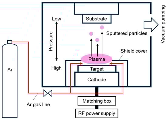
Figure 1.
Schematic diagram of PGS equipment [45].
To fabricate ternary-alloy thin films of the Bi2xSb2(1−x)Te3 system, we used a Bi8Sb31Te61 sputtering target with a 50 mm diameter and 3 mm thickness (Furuuchi Chemical, Tokyo, Japan). The atomic composition of the target was intentionally altered to deviate from its stoichiometric ratio. This was performed to ensure that the deposited thin films had a composition similar to the stoichiometric ratio, since the vapor pressures of Te and Sb are higher than those of Bi. To avoid confusion, we note that different composition notations are used for different purposes in this study: the target-based composition is used to describe the sputtering source, the normalized formula is used for comparison with conventional literature, and the alloy-based notation (Bi2xSb2(1−x)Te3) is used when discussing compositional trends. The alloy-based notation is consistently adopted for the Vegard’s law analysis. The substrate was a polished alumina substrate measuring 25 mm × 25 mm in area and 1 mm thick (AO-2525, Furuuchi Chemical, Tokyo, Japan). The PGS equipment employed in this study can accommodate four substrates in a single deposition run, thereby enabling the fabrication of four samples under strictly identical experimental conditions. For each deposition, the electrical properties (Seebeck coefficient and electrical conductivity) and film thickness of all four samples were evaluated, confirming that sample-to-sample variations were negligible. Following this verification, the first sample was assigned to nanoindentation testing, the second to XRD analysis, and the third to 3ω thermal conductivity measurements. The fourth sample was reserved as a contingency specimen to ensure continuity in the event of damage during characterization. It should be noted that the number of samples and their allocation to each measurement were identical for both the Bi2Te3 for the reference and Bi2xSb2(1−x)Te3 systems. The distance between the alumina substrate and target was maintained at 200 mm. The films were deposited on a substrate without heating. After the base pressure attained 1 × 10⁻⁴ Pa, high-purity argon gas (>99.9%) was introduced into the chamber at a flow rate of 20 sccm. While maintaining the process pressure at 0.6 Pa, measurements were performed near the substrate. Argon plasma was produced by delivering 30 W of RF power through a matching network and RF generator, with a deposition duration of 120 min. Following film growth, thermal annealing was carried out to improve crystallinity. The substrate was placed in an electric furnace containing a mixture of 5% hydrogen and 95% argon at atmospheric pressure. The furnace was heated to 573 K, and the substrate was annealed for 1 h.
The thickness and surface morphology of the films were measured with a Dektak XT stylus profiler (Bruker, Billerica, MA, USA) and white-light interferometry (BW-S507, Nikon, Tokyo, Japan), respectively. An electron-probe microanalyzer (EPMA-8050G, Shimadzu, Kyoto, Japan) was used to analyze the atomic compositions of the thin films. The surface morphologies of the thin films were investigated via field-emission scanning electron microscopy (FE-SEM; JSM-7100F, JEOL, Akishima, Japan). X-ray diffraction (XRD; Mini Flex II, Rigaku, Akishima, Japan) with Cu–Kα radiation (λ = 0.154 nm, 2θ range of 7–80°) was utilized to examine the crystallographic features of the thin films. Average crystallite size and orientation were assessed using Rietveld refinement along with evaluation of XRD peaks and diffraction profiles. The sound velocity was derived from the elastic moduli, obtained through nanoindentation measurements (ENTNEXUS; ELIONIX, Hachioji, Japan) functioning under continuous stiffness mode at approximately 300 K [47]. The indentation depth was set to one-tenth of the film thickness. Detailed measurements and calculations are provided in the Supplementary Materials (Figure S1) [46].
For the evaluation of thermoelectric properties of the thin films near 300 K, electrical conductivity and the Seebeck coefficient were determined along the in-plane direction, while thermal conductivity was assessed in the cross-plane orientation. Another direction of the thermoelectric properties were calculated based on the anisotropic properties of bismuth–telluride-based alloys, as described in our previous report [48]. The in-plane Seebeck coefficient was measured using a home-built setup. A heat sink was attached to one end of the film and a heater to the other. The centers of the thin films were pressed with two 0.1 mm-diameter K-type thermocouples separated by 13 mm. A temperature difference ranging from 1 to 4 K was applied between the thermocouples, and the Seebeck voltage was recorded at 1 K steps with a temperature reader (GR-3500, KEYENCE, Osaka, Japan) and a digital multimeter (R6561, ADVANTEST, Tokyo, Japan). The Seebeck coefficient of each sample was measured four times. Subsequently, the average value was calculated. Electrical resistance was measured using a four-point probe method (RT-70V, Napson, Tokyo, Japan), and the in-plane electrical conductivity was determined based on the measured film thickness and electrical resistance. The electrical conductivity of each sample was measured four times. Subsequently, the average value was calculated. The power factor (S2σ) was determined using the measured Seebeck coefficient (S) and electrical conductivity (σ). The cross-plane thermal conductivity was measured using the 3ω method. Detailed measurements are provided in the Supplementary Materials (Figure S2) [49]. The dimensionless figure of merit ZT, which is represented by S2σT/κ, was determined at 300 K using the power factor, absolute temperature (T), and thermal conductivity (κ).
The phonon transport properties of the thin films near 300 K served as the basis for estimating the lattice thermal conductivity and phonon MFP. Specifically, the lattice thermal conductivity was obtained by subtracting the electronic thermal conductivity from the total thermal conductivity, which was measured using the 3ω method, whereas the electronic thermal conductivity was determined based on the Wiedemann–Franz law and the measured electrical conductivity. The phonon MFP was obtained by dividing the lattice thermal conductivity by the specific heat and sound velocity.
3. Results and Discussion
3.1. Structural Properties of Bismuth–Telluride-Based Alloy Thin Films
Table 1 lists the physical properties of the bismuth–telluride-based alloy thin films. For comparison, this table includes the properties of the Bi2Te3 thin film, as reported in our previous study [45]. To match the film thickness with that of the reference Bi2Te3 thin film, the thickness of the Bi2xSb2(1−x)Te3 thin film was set to 0.6 µm. The deposition rate of the Bi2xSb2(1−x)Te3 thin film was 4.7 nm/min, which is lower than that of the Bi2Te3 thin film. The composition of the Bi2xSb2(1−x)Te3 thin film was as follows: 9.5 at.% Bi, 32.2 at.% Sb, and 58.3 at.% Te. The atomic composition ratio of the thin films deviated slightly from the stoichiometric ratio of 10 at.% Bi, 30 at.% Sb, and 60 at.% Te. However, because this composition ratio differed from the stoichiometric ratio by only 2%, the film is referred to as Bi0.5Sb1.5Te3 hereinafter. It should be noted that we confirmed that the atomic composition of bismuth antimony telluride thin films remained unchanged after thermal annealing under identical conditions in our previous study [50].

Table 1.
Physical properties of bismuth–telluride-based alloy thin films.
Figure 2 shows the surface morphologies of the bismuth–telluride-based alloy thin films. As shown in Figure 2a, the SEM image of the Bi0.5Sb1.5Te3 thin film shows steps caused by polishing scratches on the substrate. However, the film surface was extremely smooth, with no clear crystal grains or grain boundaries observed. The smooth surface of the film was confirmed via white-light interferometry, as shown in Figure 2b. Barely any voids were detected in the film, and the estimated surface roughness (Ra) was 3.1 nm. The surface SEM image of the Bi2Te3 thin film is similar to that of the Bi0.5Sb1.5Te3 thin film shown in Figure 2c; however, the surface roughness of the Bi2Te3 thin film differs from that of the Bi0.5Sb1.5Te3 thin film shown in Figure 2d. Numerous small voids were scattered across the Bi2Te3 thin film, and the measured Ra was 26.3 nm. Therefore, we demonstrated that the Bi0.5Sb1.5Te3 thin film formed using the PGS equipment was significantly smoother and contained fewer voids. This may be due to the sputtered Bi0.5Sb1.5Te3 particles being smaller and more uniform in size as compared with the Bi2Te3 particles. When large sputtered particles are included, the surface roughness of the film increases when these particles adhere to the substrate. Additionally, when the large sputtered particles fall off from the substrate, the areas remain as voids. The low deposition rate of the Bi0.5Sb1.5Te3 thin film is related to the small size of the sputtered particles. Furthermore, the mesoscale height variations in the thin films were quantitatively evaluated by acquiring thickness profile measurements with a stylus profiler (Dektak). The resulting profiles reveal that the Bi0.5Sb1.5Te3 thin film exhibits only negligible thickness fluctuations, whereas the Bi2Te3 thin film displays pronounced surface undulations consistent with the presence of numerous voids. These observations are consistent with the Ra values obtained from white-light interferometry and provide additional, independent evidence for the exceptionally smooth surface morphology of the Bi0.5Sb1.5Te3 film. The corresponding Dektak data are presented in the Supplementary Materials (Figure S3).
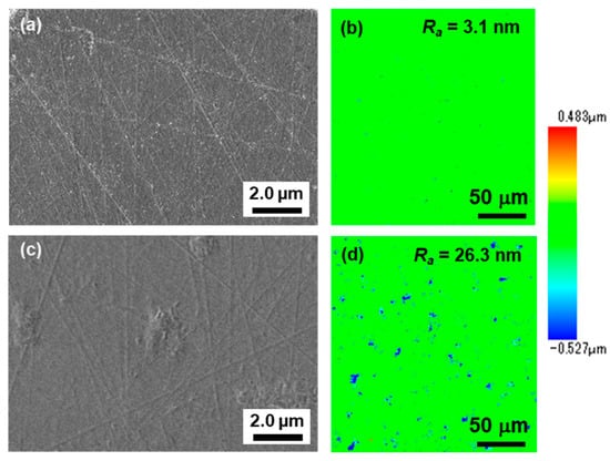
Figure 2.
(a) Surface morphology and (b) roughness of Bi0.5Sb1.5Te3 thin film analyzed via FE-SEM and white-light interferometry, respectively. (c) Surface morphology and (d) roughness of Bi2Te3 thin film.
The XRD patterns of the bismuth–telluride-based alloy thin films are shown in Figure 3a. The XRD peaks of Al2O3 originate from the substrate. Meanwhile, the XRD patterns of the Bi2Te3 and Bi0.5Sb1.5Te3 thin films matched the peaks of Bi2Te3 (JCPDS 15-0863) and Bi0.5Sb1.5Te3 (JCPDS: 49-1713), respectively. To investigate the crystal structures of the abovementioned thin films in detail, the average crystallite size and crystal orientation were evaluated by performing Rietveld analysis on the XRD patterns, as shown in Figure 3b,c, respectively. The average crystallite size was calculated using the Scherrer equation, D = Kλ/βcosθ, where D is the average crystallite size, K is the dimensionless shape factor (set as 0.89 in this study), λ the X-ray wavelength, β the line broadening at half the maximum intensity, and θ the Bragg angle [51]. The average crystallite sizes of the Bi0.5Sb1.5Te3 and Bi2Te3 thin films were 15.9 and 23.0 nm, respectively. Therefore, both thin films were composed of nanocrystals, although the Bi0.5Sb1.5Te3 thin film contained approximately 30% fewer nanocrystals than the Bi2Te3 thin film. The Lotgering factor, calculated via Equation (1) [52], was employed to analyze the crystal orientation.
where P = ΣI(00l)/ΣI(hkl), P0 = ΣI0(00l)/ΣI0(hkl), I represents the peak intensities in the experimentally obtained XRD patterns, and I0 represents the peak intensities in the XRD patterns of Bi2Te3 (JCPDS 15-0863) for the Bi2Te3 thin film and Bi0.5Sb1.5Te3 (JCPDS 49-1713) for the Bi0.5Sb1.5Te3 thin film. The F-value of the Bi2Te3 film was 0.97, thus indicating an almost perfect orientation. By contrast, the F-value of the Bi0.5Sb1.5Te3 thin film was 0.39. Therefore, when Bi in the bismuth–telluride-based alloy thin film was replaced with Sb to create an Sb-rich condition, the crystal size decreased while the crystal orientation shifted to a random orientation.
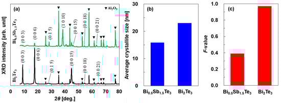
Figure 3.
(a) XRD patterns of bismuth–telluride-based alloy thin films. (b) Average crystallite size and (c) F-value of thin films obtained using Rietveld refinement.
Figure 4 shows the elastic properties of the bismuth–telluride-based alloy thin films. The Young’s moduli of the thin films were determined from their load–displacement curves, which are provided in the Supplementary Materials (Figure S4). As shown in Figure 4a, the Young’s moduli of the Bi0.5Sb1.5Te3 and Bi2Te3 thin films were 75 and 67 GPa, respectively, which did not differ significantly. The shear modulus (G) was calculated using Equation (2).
where E and ν are the Young’s modulus and Poisson’s ratio, respectively. For the Bi2Te3 thin film, a literature value of 0.23 was used as Poisson’s ratio [53]. We calculated the Poisson’s ratio for the Bi0.5Sb1.5Te3 thin film using literature values of 0.23 and 0.24 for Bi2Te3 and Sb2Te3, respectively [53]. Based on Vegard’s law, the Poisson’s ratio of the Bi0.5Sb1.5Te3 thin film was calculated to be 0.24 as it contained 25% Bi2Te3 and 75% Sb2Te3. The shear moduli of the Bi0.5Sb1.5Te3 and Bi2Te3 thin films were 30 and 27 GPa, respectively, which did not differ significantly. The longitudinal (vL) and transverse (vT) sound velocities were calculated using Equations (3) and (4), respectively [54].
where ρ denotes the mass density. For the Bi2Te3 thin film, a literature value of 7.74 g/cm3 was used. We calculated the mass density of the Bi0.5Sb1.5Te3 thin film using literature values of 7.74 and 6.51 g/cm3 for Bi2Te3 and Sb2Te3, respectively. Based on Vegard’s law, the mass density of the Bi0.5Sb1.5Te3 thin film was calculated to be 6.82 g/cm3. The average sound velocity (vave) was obtained using Equation (5).
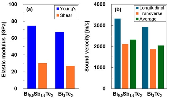
Figure 4.
(a) Elastic moduli and (b) sound velocity of bismuth–telluride-based alloy thin films.
The longitudinal, transverse, and average sound velocities of the Bi0.5Sb1.5Te3 thin films were 3320, 2115, and 2325 m/s, respectively, which are approximately 13% higher than the corresponding sound velocities of the Bi2Te3 thin film.
3.2. Thermoelectric Properties of Bismuth–Telluride-Based Alloy Thin Films
Figure 5 shows the thermoelectric properties of the bismuth–telluride-based alloy thin films measured at approximately 300 K. The Seebeck coefficients of the thin films are presented in Figure 5a. Specifically, the Seebeck coefficients in the in-plane direction are measured values, whereas those in the cross-plane direction are calculated based on the assumption that the magnitude of the Seebeck coefficient depends on the crystal orientation (F-value), as per our previous study [48]. The average Seebeck coefficient (Save) is calculated using the equation Save = (2Sin + Scross)/3, where Sin and Scross are the Seebeck coefficients in the in-plane and cross-plane directions, respectively. The Seebeck coefficients of both thin films were almost independent of the orientation. The average Seebeck coefficients of the Bi0.5Sb1.5Te3 and Bi2Te3 thin films were 213 and −104 μV/K, respectively. Therefore, by substituting Sb for Bi in bismuth-telluride-based alloy thin films to render them Sb-rich, the Seebeck coefficient changed from negative to positive, and the absolute value of the Seebeck coefficient increased twofold.
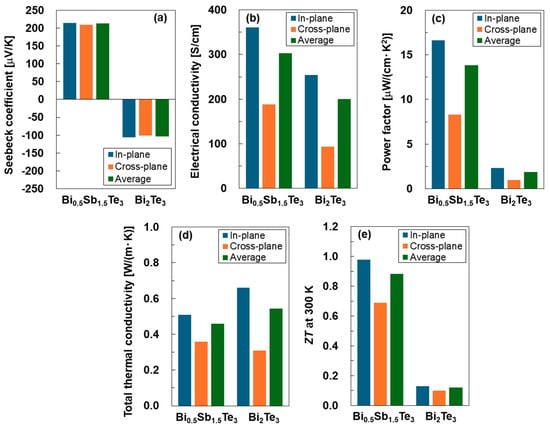
Figure 5.
Thermoelectric properties of bismuth–telluride-based alloy thin films measured at approximately 300 K: (a) Seebeck coefficient, (b) electrical conductivity, (c) power factor, (d) thermal conductivity, and (e) dimensionless figure of merit.
The electrical conductivities of the thin films are presented in Figure 5b. The electrical conductivities in the in-plane direction are measured values, whereas those in the cross-plane direction are calculated using the same assumptions as for the Seebeck coefficient [48]. Additionally, the average electrical conductivity is calculated using the same method as that used for the Seebeck coefficient. Compared with the Seebeck coefficient, the electrical conductivity is significantly affected by the direction. For the Bi0.5Sb1.5Te3 thin film, the in-plane electrical conductivity was 361 S/cm, which is 1.9 times higher than that in the cross-plane direction. Conversely, for the Bi2Te3 thin film, the in-plane electrical conductivity was 254 S/cm, which was 2.7 times higher than that in the cross-plane direction. This increase occurred because the Bi2Te3 thin film exhibited an almost perfect crystal orientation. In both directions, the Bi0.5Sb1.5Te3 thin film exhibited higher electrical conductivity than the Bi2Te3 thin film. The average electrical conductivity of the Bi0.5Sb1.5Te3 thin film was 303 S/cm, which was 1.5 times higher than that of the Bi2Te3 thin film. Therefore, by substituting Sb for Bi in bismuth–telluride-based alloy thin films to render them Sb-rich, the electrical conductivity can be increased while maintaining a high Seebeck coefficient. This is due to a change in the electronic band structure, which resulted from the shift in the alloy composition from a binary to a ternary system. This system introduces or modifies a sharp feature in the density of states near the Fermi level or band edge that determines the Seebeck coefficient, while maintaining high carrier mobility [55,56].
The power factors of the thin films are presented in Figure 5c. The Seebeck coefficient and electrical conductivity were measured in the in-plane direction, whereas the power factor in the in-plane direction was regarded as the measured value. The power factors of the Bi0.5Sb1.5Te3 thin film increased significantly in all directions owing to its high Seebeck coefficient and electrical conductivity. In particular, the in-plane power factor of the Bi0.5Sb1.5Te3 thin film reached 16.6 μW/(cm·K2), which was 7.2 times higher than that of the Bi2Te3 thin film in the corresponding direction. However, the highest power factor in this study remained lower than that of established bismuth–telluride-based alloys reported in previous studies [57,58,59].
The thermal conductivities of the thin films are presented in Figure 5d. In contrast to the Seebeck coefficient and electrical conductivity, the thermal conductivity in the cross-plane direction was the measured value. Estimating the in-plane thermal conductivity is more complicated than estimating the Seebeck coefficient and electrical conductivity because the measured thermal conductivity, namely, the total thermal conductivity (κtot), includes the electronic thermal conductivity (κele) and lattice thermal conductivity (κlat). The electronic thermal conductivity was calculated using the Wiedemann–Franz law, as expressed in Equation (6) [60].
where L, σ, and T denote the Lorentz number, electrical conductivity, and absolute temperature, respectively. The Lorentz numbers were calculated using Equation (7) [61,62].
where |S| is the absolute value of the Seebeck coefficient. This equation is widely used to estimate the Lorenz number from the Seebeck coefficient in degenerate and near-degenerate semiconductors. Therefore, to estimate the in-plane κtot, the in-plane κele was calculated using the measured electrical conductivity in the in-plane direction and the Wiedemann–Franz law. The in-plane κlat was calculated based on the assumption that the magnitude of κlat depends on the crystal orientation (F-value), as per our previous study [48]. Consequently, the in-plane ktot was determined by adding the in-plane kele and klat. The measured cross-plane ktot of the Bi0.5Sb1.5Te3 thin film was 0.36 W/(m·K), which was higher than that of the Bi2Te3 thin film (0.31 W/(m·K)). However, the calculated in-plane κtot of the Bi0.5Sb1.5Te3 thin film was 0.51 W/(m·K), which was lower than that of the Bi2Te3 thin film (0.66 W/(m·K)). These results were obtained because the crystal orientation of the Bi0.5Sb1.5Te3 thin film was lower than that of the Bi2Te3 thin film. The average κtot of the Bi0.5Sb1.5Te3 thin film was 0.46 W/(m·K), which was 15% lower than that of the Bi2Te3 thin film.
The dimensionless figure of merit, ZT, for the thin films is shown in Figure 5e. The Bi0.5Sb1.5Te3 thin film exhibited a significantly high ZT in all directions owing to its high power factor and low thermal conductivity. In particular, the in-plane ZT of the Bi0.5Sb1.5Te3 thin film reached 0.98, which was 7.5 times higher than that of the Bi2Te3 thin film in the corresponding direction. Therefore, using the PGS equipment, we demonstrated that the thermoelectric performance can be significantly improved by replacing Bi in a bismuth–telluride-based alloy thin film with Sb, thereby creating an Sb-rich condition. Although the ZT of the Bi0.5Sb1.5Te3 thin film in this study is inferior to that of Sb2Te3/Bi2Te3 superlattice thin films [63], the achieved ZT is one of the highest values reported for thermoelectric materials measured near 300 K, as shown in Table 2 [64,65,66,67,68].
Table 2.
Comparison of ZT of bismuth–telluride-based alloys fabricated by different methods.
3.3. Phonon Transport Properties of Bismuth–Telluride-Based Alloy Thin Films
The phonon-transport properties of the bismuth–telluride-based alloy thin films are shown in Figure 6. The average κlat values of the thin films are shown in Figure 6a. The in-plane and cross-plane κlat values were calculated by subtracting the corresponding κele values from κtot. The average κlat was estimated using the in-plane and cross-plane κlat by employing the same method used for determining the Seebeck coefficient and electrical conductivity [48]. The average κlat of the Bi0.5Sb1.5Te3 thin film was 0.28 W/(m·K), which was approximately half of that of the Bi2Te3 thin film. The average phonon MFPs of the thin films are shown in Figure 6b. The phonon MFP (Λ) was calculated using the average sound velocity (vave) and lattice thermal conductivity (κlat), as shown in Equation (8).
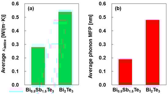
Figure 6.
Phonon-transport properties of bismuth–telluride-based alloy thin films: (a) lattice thermal conductivity and (b) phonon MFP.
Here, C is the specific heat, which was assigned a value of 165 J/(kg·K) for the Bi2Te3 thin film [69]. The specific heat for the Bi0.5Sb1.5Te3 thin film was calculated using literature values of 165 and 203 J/(kg·K) for Bi2Te3 and Sb2Te3, respectively [69,70]. Based on Vegard’s law, the specific heat of the Bi0.5Sb1.5Te3 thin film was determined to be 191 J/(kg·K). Consequently, the average phonon MFPs for the Bi0.5Sb1.5Te3 and Bi2Te3 thin films were determined to be 0.19 and 0.48 nm, respectively. These values are markedly smaller than the corresponding crystallite sizes shown in Figure 3b, indicating that phonon transport in both films is dominated by intracrystalline scattering mechanisms rather than by boundary scattering. Notably, the substantially shorter phonon MFP observed in the Bi0.5Sb1.5Te3 film highlights the pronounced influence of alloy-induced phonon scattering, which becomes significant upon introducing Sb into the Bi–Te lattice. This behavior is consistent with previous reports on bulk and thin-film Bi–Sb–Te systems, where mass-fluctuation scattering is known to play a central role in reducing lattice thermal conductivity [71]. To aid interpretation, we note that the relatively short phonon MFPs obtained in this study reflect the strong phonon scattering characteristic of sputter-deposited bismuth antimony telluride films and remain consistent with values reported for comparably disordered systems [72]. In addition, the estimation procedure relies on bulk values for density, specific heat, and Poisson’s ratio, and the measured thermal conductivity is subject to underestimation owing to thermal boundary resistance at both the heater/film and film/substrate interfaces. These factors have the potential to shift the absolute phonon MFP values toward the lower bound; nevertheless, they do not affect the comparative trends that constitute the basis of our analysis. Although a complete spectral decomposition lies beyond the scope of the present work, the average phonon MFP extracted here reflects a strongly scattered transport regime and falls near the lower bound of the spectral MFP distributions reported for comparable materials [73,74].
4. Conclusions
We prepared Bi0.5Sb1.5Te3 thin films using a PGS equipment and investigated their properties by comparing them with those of Bi2Te3 thin films prepared using the same system, as reported in our previous study. The Bi0.5Sb1.5Te3 thin film comprised nanocrystals with an average size of 15.9 nm and exhibited a remarkably smooth surface with a roughness of 3.1 nm. The Bi0.5Sb1.5Te3 thin film did not indicate a preferred crystal orientation, whereas the Bi2Te3 thin film showed an almost perfect crystal orientation. When the elastic moduli and sound velocities were analyzed based on nanoindentation, no significant differences were observed between the Bi0.5Sb1.5Te3 and Bi2Te3 thin films. However, their thermoelectric properties differed significantly. By substituting Sb for Bi in the Bi2Te3 thin film to form a Bi0.5Sb1.5Te3 thin film, the Seebeck coefficient changed from negative to positive and the absolute value of the Seebeck coefficient increased two-fold. The thermal conductivities of the thin films were measured using the 3ω method. The measured cross-plane κtot of the Bi0.5Sb1.5Te3 thin film was higher than that of the Bi2Te3 thin film, whereas the calculated in-plane κtot of the Bi0.5Sb1.5Te3 thin film was lower than that of the Bi2Te3 thin film. The Bi0.5Sb1.5Te3 thin film exhibited an in-plane ZT value of 0.98, which was 7.5 times higher than that of the Bi2Te3 thin film in the same direction. Notably, it is one of the highest values reported for thermoelectric materials measured near 300 K. The average phonon MFPs of the Bi0.5Sb1.5Te3 and Bi2Te3 thin films were obtained as 0.19 and 0.48 nm, respectively. Because the phonon MFPs were significantly smaller than the average crystallite size of the thin films, phonon scattering occurred more frequently via alloy scattering inside the crystallite than via boundary scattering at the crystallite boundaries. In particular, the phonon MFP decreased owing to ternary-alloy scattering in the Bi0.5Sb1.5Te3 thin film. The results of this study can advance thin-film TEGs as a source of self-sustaining power for IoT systems.
Supplementary Materials
The following information can be downloaded from https://www.mdpi.com/article/10.3390/coatings16010035/s1: Figure S1: Principle diagram of nanoindentation method, where the reference [46] is cited in the Supplementary Materials. Figure S2: Principle diagram of 3ω method, where the reference [49] is cited in the Supplementary Materials. Figure S3: Thickness profile of (a) Bi0.5Sb1.5Te3 and (b) Bi2Te3 thin films. Figure S4: Load–displacement curves of (a) Bi0.5Sb1.5Te3 and (b) Bi2Te3 thin films.
Author Contributions
Conceptualization, M.T.; methodology, T.T., Y.N., K.K., Y.S., T.K. and H.M.; investigation, T.T., Y.N., K.K., Y.S., T.K. and H.M.; writing—original draft, T.T., K.K., Y.S., C.Z. and M.T.; supervision, M.T.; project administration, M.T.; Funding acquisition, M.T. All authors have read and agreed to the published version of the manuscript.
Funding
This study was partially supported by the JSPS KAKENHI (grant number 22H04953).
Institutional Review Board Statement
Not applicable.
Informed Consent Statement
Not applicable.
Data Availability Statement
Data is contained within the article or Supplementary Materials.
Acknowledgments
All authors thank K. Yonezawa at Kenix for providing the PGS equipment, and M. Morikawa, Y. Oda, S. Yonezawa, and T. Komori at Tokai University for their experimental support.
Conflicts of Interest
The authors declare no conflicts of interest.
References
- Rosch, A.G.; Gall, A.; Aslan, S.; Hecht, M.; Franke, L.; Mallick, M.M.; Penth, L.; Bahro, D.; Friderich, D.; Lemmer, U. Fully printed origami thermoelectric generators for energy-harvesting. npj Flex. Electron. 2021, 5, 1. [Google Scholar] [CrossRef]
- Feng, M.; Lv, S.; Deng, J.; Guo, Y.; Wu, Y.; Shi, G.; Zhang, M. An overview of environmental energy harvesting by thermoelectric generators. Renew. Sustain. Energy Rev. 2023, 187, 113723. [Google Scholar] [CrossRef]
- Ando Junior, O.H.; Maran, A.L.O.; Henao, N.C. A review of the development and applications of thermoelectric microgenerators for energy harvesting. Renew. Sustain. Energy Rev. 2018, 91, 376–393. [Google Scholar] [CrossRef]
- Liu, Y.; Riba, J.R.; Eguilaz, M.M.; Sanllehi, J. Application of thermoelectric generators for low-temperature-gradient energy harvesting. Appl. Sci. 2023, 13, 2603. [Google Scholar] [CrossRef]
- Yamamoto, H.; Amezawa, T.; Okano, Y.; Hoshino, K.; Ochiai, S.; Sunaga, K.; Miyake, S.; Takashiri, M. High thermal durability and thermoelectric performance with ultra-low thermal conductivity in n-type single-walled carbon nanotube films by controlling dopant concentration with cationic surfactant. Appl. Phys. Lett. 2025, 126, 063902. [Google Scholar] [CrossRef]
- Sasi, V.T.; Machinao, S.; Thushara, R.; Veettil, A.A.; Alagarasan, D.; Pal, V.; Aravindan, M.K.; Srinivasan, B.; Karuppannan, R.; Rapaka, S.C.B. High-performance flexible thermoelectric generator via rapid evaporation of nanocrystalline Bi2Te3-alloy films. ACS Appl. Energy Mater. 2025, 8, 13185–13190. [Google Scholar] [CrossRef]
- Tao, X.; Zheng, Q.; Zeng, C.; Potter, H.; Zhang, Z.; Ellingford, J.; Bonilla, R.S.; Bilotti, E.; Grant, P.S.; Assender, H.E. Cu- or Ag-containing Bi-Sb-Te for in-line roll-to-roll patterned thin-film thermoelectrics. Nat. Commun. 2025, 16, 196. [Google Scholar] [CrossRef]
- Chatterjee, K.; Ghosh, T.K. Thermoelectric materials for textile applications. Molecules 2021, 26, 3154. [Google Scholar] [CrossRef]
- Takashiri, M.; Kurita, K.; Hagino, H.; Tanaka, S.; Miyazaki, K. Enhanced thermoelectric properties of phase-separating bismuth selenium telluride thin films via a two-step method. J. Appl. Phys. 2015, 118, 065301. [Google Scholar] [CrossRef]
- Inamoto, T.; Takashiri, M. Experimental and first-principles study of the electronic transport properties of strained Bi2Te3 thin films on a flexible substrate. J. Appl. Phys. 2016, 120, 125105. [Google Scholar] [CrossRef]
- Kim, S.; Mo, J.H.; Jang, K.S. Solution-processed carbon nanotube buckypapers for foldable thermoelectric generators. ACS Appl. Mater. Interfaces 2019, 11, 35675–35682. [Google Scholar] [CrossRef]
- Mytafides, C.K.; Tzounis, L.; Karalis, G.; Formanek, P.; Paipetis, A.S. Fully printed and flexible carbon nanotube-based thermoelectric generator capable for high-temperature applications. J. Power Sources 2021, 507, 230323. [Google Scholar] [CrossRef]
- Muchuweni, E.; Mombeshora, E.T. Enhanced thermoelectric performance by single-walled carbon nanotube composites for thermoelectric generators: A review. Appl. Surf. Sci. Adv. 2023, 13, 100379. [Google Scholar] [CrossRef]
- Chiba, T.; Yabuki, H.; Takashiri, M. High thermoelectric performance of flexible nanocomposite films based on Bi2Te3 nanoplates and carbon nanotubes selected using ultracentrifugation. Sci. Rep. 2023, 13, 3010. [Google Scholar] [CrossRef]
- Norimasa, O.; Tamai, R.; Nakayama, H.; Shinozaki, Y.; Takashiri, M. Self-generated temperature gradient under uniform heating in p–i–n junction carbon nanotube thermoelectric generators. Sci. Rep. 2025, 15, 15956. [Google Scholar] [PubMed]
- Glatz, W.; Muntwyler, S.; Hierold, C. Optimization and fabrication of thick flexible polymer based micro thermoelectric generator. Sens. Actuators 2006, 132, 337–345. [Google Scholar]
- Menon, A.K.; Yee, S.K. Design of a polymer thermoelectric generator using radial architecture. J. Appl. Phys. 2016, 119, 055501. [Google Scholar] [CrossRef]
- Lund, A.; Tian, Y.; Darabi, S.; Müller, C. A polymer-based textile thermoelectric generator for wearable energy harvesting. J. Power Sources 2020, 480, 228836. [Google Scholar] [CrossRef]
- Elmoughni, H.M.; Menon, A.K.; Wolfe, R.M.W.; Yee, S.K. A textile-integrated polymer thermoelectric generator for body heat harvesting. Adv. Mater. Technol. 2019, 4, 1800708. [Google Scholar] [CrossRef]
- Hou, Y.-C.; Huang, M.-J.; Chuang, P.-Y.; Chang, H.-C.; Chen, C.-H. Numerical and model predictions of the thermal conductivity of bismuth telluride nanoprism-assembled films. Int. J. Heat Mass Transf. 2015, 87, 536–543. [Google Scholar] [CrossRef]
- Chen, T.-H.; Chen, P.-H.; Chen, C.-H. Laser co-ablation of bismuth antimony telluride and diamond-like carbon nanocomposites for enhanced thermoelectric performance. J. Mater. Chem. A 2018, 6, 982–990. [Google Scholar] [CrossRef]
- Karimov, K.S.; Fatima, N.; Qasuria, T.A.; Siddiqui, K.J.; Bashir, M.M.; Alharbi, H.F.; Alharth, N.H.; Al-Harthi, Y.S.; Amin, N.; Akhtaruzzaman, M. Innovative semitransparent photo-thermoelectric cells based on bismuth antimony telluride alloy. J. Alloys Compd. 2020, 816, 152593. [Google Scholar] [CrossRef]
- Witting, I.T.; Grovogui, J.A.; Dravid, V.P.; Snyder, G.J. Thermoelectric transport enhancement of Te-rich bismuth antimony telluride (Bi0.5Sb1.5Te3+x) through controlled porosity. J. Mater. 2020, 6, 532–544. [Google Scholar] [CrossRef]
- Fu, L.; Park, K.; Kim, S.I.; Kim, B.; Song, H.Y.; Choi, W.; Kim, Y.M. High-performance bismuth antimony telluride thermoelectric membrane on curved and flexible supports. ACS Energy Lett. 2021, 6, 7. [Google Scholar] [CrossRef]
- Jiang, J.; Chen, L.; Bai, S.; Yao, Q.; Wang, Q. Thermoelectric properties of p-type (Bi2Te3)x(Sb2Te3)1−x crystals prepared via zone melting. J. Cryst. Growth 2005, 277, 258–263. [Google Scholar] [CrossRef]
- Yang, J.; Aizawa, T.; Yamamoto, A.; Ohta, T. Thermoelectric properties of p-type (Bi2Te3)x(Sb2Te3)1−x prepared by bulk mechanical alloying and hot pressing. J. Alloys Compd. 2000, 309, 225–228. [Google Scholar] [CrossRef]
- Frari, D.D.; Diliberto, S.; Stein, N.; Boulanger, C.; Lecuire, J.M. Comparative study of the electrochemical preparation of Bi2Te3, Sb2Te3, and (BixSb1−x)2Te3 films. Thin Solid Films 2005, 483, 44–49. [Google Scholar] [CrossRef]
- Adam, A.M.; Diab, A.K.; Ataalla, M.; Alotaibi, M.F.; Alharbi, A.N.; Elsehly, E.M. Optimized thermoelectric performance in thin (Bi2Se3)1−x(Bi2Te3)x alloyed films. J. Alloys Compd. 2022, 898, 162888. [Google Scholar] [CrossRef]
- Yang, J.Y.; Aizawa, T.; Yamamoto, A.; Ohta, T. Thermoelectric properties of n-type (Bi2Se3)x(Bi2Te3)1−x prepared by bulk mechanical alloying and hot pressing. J. Alloys Compd. 2000, 312, 326–330. [Google Scholar] [CrossRef]
- Adam, A.M.; Diab, A.K.; Tolan, M.; El-Qahtani, Z.M.H.; Refaat, A.A.; El-Hadek, M.A.; Elsehly, E.M.; El-Khouly, A.; Alharbi, A.N.; Khovaylo, V.; et al. Outstanding optical properties of thermally grown (Bi2Se3)1−x(Bi2Te3)x thin films. Mater. Sci. Semicond. Process. 2022, 143, 106557. [Google Scholar] [CrossRef]
- Hu, L.-P.; Zhu, T.-J.; Wang, Y.-G.; Xie, H.-H.; Xu, Z.-J.; Zhao, X.-B.; Zhao, X.-B. Shifting up the optimum figure of merit of p-type bismuth telluride-based thermoelectric materials for power generation by suppressing intrinsic conduction. NPG Asia Mater. 2014, 6, e88. [Google Scholar] [CrossRef]
- Boulouz, A.; Chakraborty, S.; Giani, A.; Delannoy, F.P.; Boyer, A.; Schumann, J. Transport properties of V–VI semiconducting thermoelectric BiSbTe alloy thin films and their application to micromodule Peltier devices. J. Appl. Phys. 2001, 89, 5009–5014. [Google Scholar] [CrossRef]
- Zheng, G.; Su, X.; Liang, T.; Lu, Q.; Yan, Y.; Uher, C.; Tang, X. High thermoelectric performance of mechanically robust n-type Bi2Te3−xSex prepared by combustion synthesis. J. Mater. Chem. A 2015, 3, 6603–6613. [Google Scholar] [CrossRef]
- Sánchez, F.S.; Gharsallah, M.; Nemes, N.M.; Biskup, N.; Varela, M.; Martínez, J.L.; Fernández-Díaz, M.T.; Alonso, J.A. Enhanced figure of merit in nanostructured (Bi,Sb)2Te3 with optimized composition, prepared by a straightforward arc-melting procedure. Sci. Rep. 2017, 7, 6277. [Google Scholar] [CrossRef] [PubMed]
- Bourgault, D.; Garampon, C.G.; Caillault, N.; Carbone, L.; Aymami, J.A. Thermoelectric properties of n-type Bi2Te2.7Se0.3 and p-type Bi0.5Sb1.5Te3 thin films deposited by direct current magnetron sputtering. Thin Solid Films 2008, 516, 8579–8583. [Google Scholar] [CrossRef]
- Somdock, N.; Kianwimol, S.; Harnwunggmoung, A.; Sakulkalavek, A.; Sakdanuphab, R. Simultaneous stoichiometric composition and highly (00l) orientation of flexible Bi2Te3 thin films via optimising the DC magnetron sputter-deposition process. J. Alloys Compd. 2019, 773, 78–85. [Google Scholar] [CrossRef]
- Uchino, M.; Kato, K.; Hagino, H.; Miyazaki, K. Fabrication by coaxial-type vacuum arc evaporation method and characterization of bismuth telluride thin films. J. Electron. Mater. 2013, 42, 1814–1819. [Google Scholar] [CrossRef]
- Singh, S.; Singh, J.; Kaushal, J.; Tripathi, S.K. Effects of annealing on the thermoelectric properties of nanocrystalline Bi1.2Sb0.8Te3 thin films prepared by thermal evaporation. Appl. Phys. A 2019, 125, 144. [Google Scholar] [CrossRef]
- Kuleshova, J.; Koukharenko, E.; Li, X.; Frety, N.; Nandhakumar, I.S.; Tudor, J.; Beeby, S.P.; White, N.M. Optimization of the electrodeposition process of high-performance bismuth antimony telluride compounds for thermoelectric applications. Langmuir 2010, 26, 16980–16985. [Google Scholar] [CrossRef] [PubMed]
- Su, N.; Guo, S.; Li, F.; Li, B. Electrodeposition of Bi-Te thin films on silicon wafer and micro-column arrays on microporous glass template. Nanomaterials 2020, 10, 431. [Google Scholar] [CrossRef]
- Takashiri, M.; Tanaka, S.; Miyazaki, K. Determination of the origin of crystal orientation for nanocrystalline bismuth telluride-based thin films prepared by use of the flash evaporation method. J. Electron. Mater. 2014, 43, 1881–1889. [Google Scholar] [CrossRef]
- Terai, Y.; Haraguchi, K.; Ichinose, R.; Oota, H.; Yonezawa, K. Structural and piezoelectric properties of AlN thin films grown by pressure gradient sputtering. Jpn. J. Appl. Phys. 2023, 62, SA1003. [Google Scholar]
- Aono, M.; Terauchi, M.; Sato, Y.K.; Morita, K.; Inoue, T.; Kanda, K.; Yonezawa, K. Deposition of amorphous carbon nitride thin films using pressure-gradient RF magnetron sputtering and their chemical bonding structures. Appl. Surf. Sci. 2023, 635, 157677. [Google Scholar] [CrossRef]
- Abe, Y.; Nishimura, T.; Yamada, A. Impacts of O2/(O2+Ar) Flow ratio on the properties of Li-doped NiO thin films fabricated by pressure-gradient radiofrequency magnetron sputtering. Phys. Status Solidi A 2025, 222, 2400497. [Google Scholar] [CrossRef]
- Takizawa, T.; Kaneko, K.; Shinozaki, Y.; Kaneko, T.; Murotani, H.; Takashiri, M. Nearly perfect crystal orientation of nanocrystalline bismuth telluride thin films deposited by pressure-gradient sputtering and their thermal transport properties. Coatings 2025, 15, 1234. [Google Scholar] [CrossRef]
- Hase, M.; Tanisawa, D.; Kohashi, K.; Kamemura, R.; Miyake, S.; Takashiri, M. Determination of Seebeck coefficient originating from phonon-drag effect using Si single crystals at different carrier densities. Sci. Rep. 2023, 13, 13463. [Google Scholar] [CrossRef]
- Oliver, W.C.; Pharr, G.M. An improved technique for determining hardness and elastic modulus using load and displacement sensing indentation experiments. J. Mater. Res. 1992, 7, 1564–1583. [Google Scholar] [CrossRef]
- Kudo, S.; Tanaka, S.; Miyazaki, K.; Nishi, Y.; Takashiri, M. Anisotropic analysis of nanocrystalline bismuth telluride thin films treated by homogeneous electron beam irradiation. Mater. Trans. 2017, 58, 513–519. [Google Scholar] [CrossRef]
- Kudo, S.; Hagino, H.; Tanaka, S.; Miyazaki, K.; Takashiri, M. Determining the thermal conductivities of nanocrystalline bismuth telluride thin films using the differential 3ω method while accounting for thermal contact resistance. J. Electron. Mater. 2015, 44, 2021–2025. [Google Scholar] [CrossRef]
- Hatsuta, N.; Takemori, D.; Takashiri, M. Effect of thermal annealing on the structural and thermoelectric properties of electrodeposited antimony telluride thin films. J. Alloys Compd. 2016, 685, 147–152. [Google Scholar] [CrossRef]
- Cullity, B.D. Elements of X-Ray Diffraction, 2nd ed.; Addison-Wesley Publishing: Boston, MA, USA, 1956. [Google Scholar]
- Lotgering, F.K. Topotactical reactions with ferrimagnetic oxides having hexagonal crystal structures—I. J. Inorg. Nucl. Chem. 1959, 9, 113–123. [Google Scholar] [CrossRef]
- Fu, J.; Huang, J.; Bernard, F. Electronic structure, elastic and optical properties of Bi2Te3/Sb2Te3 thermoelectric composites in the periodic-superlattice thin films. Compos. Commun. 2021, 28, 100917. [Google Scholar] [CrossRef]
- Cordier, J.-P. Velocities in Reflection Seismology, 1st ed.; Springer: Dordrecht, The Netherlands, 1985; pp. 14–24. [Google Scholar]
- Jiang, Y.; Yu, J.; Li, H.; Zhuanga, H.-L.; Li, J.-F. Chemical modulation and defect engineering in high-performance GeTe-based thermoelectrics. Chem. Sci. 2025, 16, 1617–1651. [Google Scholar] [CrossRef] [PubMed]
- Su, L.; Shi, H.; Wang, S.; Wang, D.; Qin, B.; Wang, Y.; Chang, C.; Zhao, L.-D. Enhancing carrier mobility and Seebeck coefficient by modifying scattering factor. Adv. Energy Mater. 2023, 13, 2300312. [Google Scholar] [CrossRef]
- Cha, J.; Zhou, C.; Cho, S.-P.; Park, S.H.; Chung, I. Ultrahigh power factor and electron mobility in n-type Bi2Te3−x%Cu stabilized under excess Te condition. ACS Appl. Mater. Interfaces 2019, 11, 30999–31008. [Google Scholar] [CrossRef] [PubMed]
- Winkler, M.; Liu, X.; Schürmann, U.; König, J.D.; Kienle, L.; Bensch, W.; Böttner, H. Current status in fabrication, structural and transport property characterization, and theoretical understanding of Bi2Te3/Sb2Te3 superlattice systems. Z. Anorg. Allg. Chem. 2012, 638, 2441–2454. [Google Scholar] [CrossRef]
- Symeou, E.; Nicolaou, C.; Delimitis, A.; Androulakis, J.; Kyratsi, T.; Giapintzakis, J. High thermoelectric performance of Bi2−xSbxTe3 bulk alloys prepared from non-nanostructured starting powders. J. Solid State Chem. 2019, 270, 388–397. [Google Scholar] [CrossRef]
- Wei, M.; Li, H.; Nisar, M.; Zhang, Z.; Li, F.; Liang, G.; Luo, J.; Zheng, Z.; Chen, Y.; Zheng, Z. The synergistic effect of hole co-doping on carrier transports and phonon tuning in Sb2Te3 flexible thermoelectric thin film. Chem. Eng. J. 2024, 495, 153185. [Google Scholar] [CrossRef]
- Wilson, R.B.; Cahill, D.G. Experimental validation of the interfacial form of the Wiedemann-Franz law. Phys. Rev. Lett. 2012, 108, 255901. [Google Scholar] [CrossRef]
- Kim, H.-S.; Zachary, M.G.; Tang, Y.; Wang, H.; Snyder, G.S. Characterization of Lorenz number with Seebeck coefficient measurement. APL Mater. 2015, 3, 041506. [Google Scholar] [CrossRef]
- Venkatasubramanian, R.; Siivola, E.; Colpitts, T.; O’quinn, B. Thin-film thermoelectric devices with high room-temperature figures of merit. Nature 2001, 413, 597–602. [Google Scholar] [CrossRef]
- Poudel, B.; Hao, Q.; Ma, Y.; Lan, Y.; Minnich, A.; Yu, B.; Yan, X.; Wang, D.; Muto, A.; Vashaee, D. High-thermoelectric performance of nanostructured bismuth antimony telluride bulk alloys. Science 2008, 320, 634–638. [Google Scholar] [CrossRef] [PubMed]
- Chung, D.-Y.; Hogan, T.; Brazis, P.; Rocci-Lane, M.; Kannewurf, C.; Bastea, M.; Uher, C.; Kanatzidis, M.G. CsBi4Te6: A high-performance thermoelectric material for low-temperature applications. Science 2000, 287, 1024–1027. [Google Scholar] [CrossRef] [PubMed]
- Li, D.; Sun, L.L.; Qin, X.Y. Thermoelectric properties of p-type (Bi2Te3)x(Sb2Te3)1−x prepared by spark plasma sintering. Intermetallics 2011, 19, 2002–2005. [Google Scholar] [CrossRef]
- Scheele, M.; Oeschler, N.; Veremchuk, I.; Reinsberg, K.-G.; Kreuziger, A.-M.; Kornowski, A.; Broekaert, J.; Klinke, C.; Weller, H. ZT enhancement in solution-grown Sb(2−x)BixTe3 nanoplatelets. ACS Nano 2010, 4, 4283–4291. [Google Scholar] [CrossRef]
- Wei, M.; Shi, X.-L.; Zheng, Z.-H.; Li, F.; Liu, W.-D.; Xiang, L.-P.; Xie, Y.-S.; Chen, Y.-X.; Duan, J.-Y.; Ma, H.-L.; et al. Directional thermal diffusion realizing inorganic Sb2Te3/Te hybrid thin films with high thermoelectric performance and flexibility. Adv. Funct. Mater. 2022, 32, 2207903. [Google Scholar] [CrossRef]
- Arisaka, T.; Otsuka, M.; Hasegawa, Y. Measurement of thermal conductivity and specific heat by impedance spectroscopy of Bi2Te3 thermoelectric element. Rev. Sci. Instrum. 2019, 90, 046104. [Google Scholar] [CrossRef]
- Pattamatta, A.; Madnia, C.K. Modeling heat transfer in Bi2Te3–Sb2Te3 nanostructures. Int. J. Heat Mass Transf. 2009, 52, 860–869. [Google Scholar] [CrossRef]
- Liu, X.-D.; Park, Y.-H. Structure and transport properties of (Bi1−xSbx)2Te3 thermoelectric materials prepared by mechanical alloying and pulse discharge sintering. Mater. Trans. 2002, 43, 681–687. [Google Scholar]
- Wang, Y.; Liebig, C.; Xu, X.; Venkatasubramanian, R. Acoustic phonon scattering in Bi2Te3/Sb2Te3 superlattices. Appl. Phys. Lett. 2010, 97, 073108. [Google Scholar] [CrossRef]
- Zhang, P.; Zhang, Z.; Liu, Y.; Wang, Z.; Lu, Z.; Xiong, Z. Phonon thermal transport in Bi2Te3 from a deep-neural-network interatomic potential. Phys. Rev. Appl. 2022, 18, 054022. [Google Scholar] [CrossRef]
- Zeng, L.; Collins, K.C.; Hu, Y.; Luckyanova, M.N.; Maznev, A.A.; Huberman, S.; Chiloyan, V.; Zhou, J.; Huang, X.; Nelson, K.A.; et al. Measuring phonon mean free path distributions by probing quasiballistic phonon transport in grating nanostructures. Sci. Rep. 2015, 5, 17131. [Google Scholar] [CrossRef] [PubMed]


Disclaimer/Publisher’s Note: The statements, opinions and data contained in all publications are solely those of the individual author(s) and contributor(s) and not of MDPI and/or the editor(s). MDPI and/or the editor(s) disclaim responsibility for any injury to people or property resulting from any ideas, methods, instructions or products referred to in the content. |
© 2025 by the authors. Licensee MDPI, Basel, Switzerland. This article is an open access article distributed under the terms and conditions of the Creative Commons Attribution (CC BY) license.