
Machine Learning Optimization of Auxiliary Cathode Structure for Thickness Uniformity in Micro-Electroforming


Abstract
1. Introduction
2. Methods
2.1. Electroforming Model
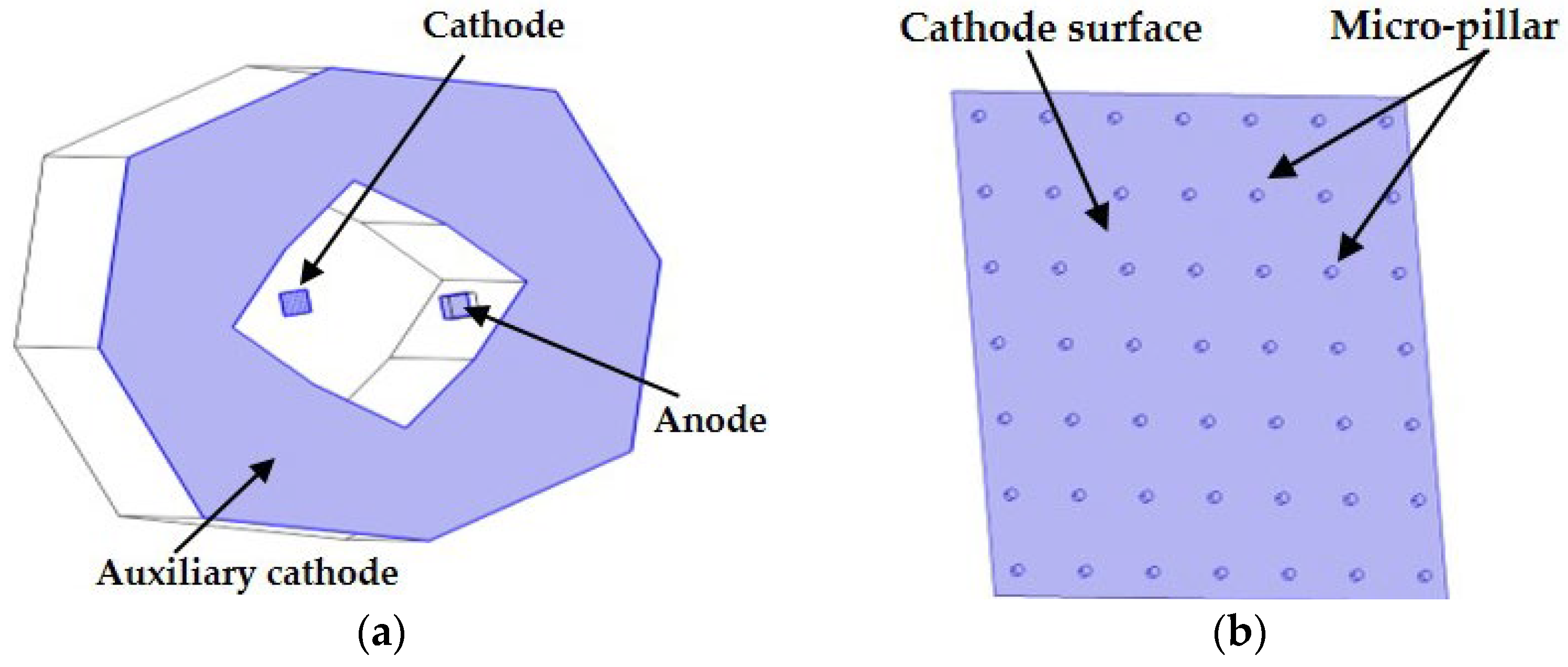
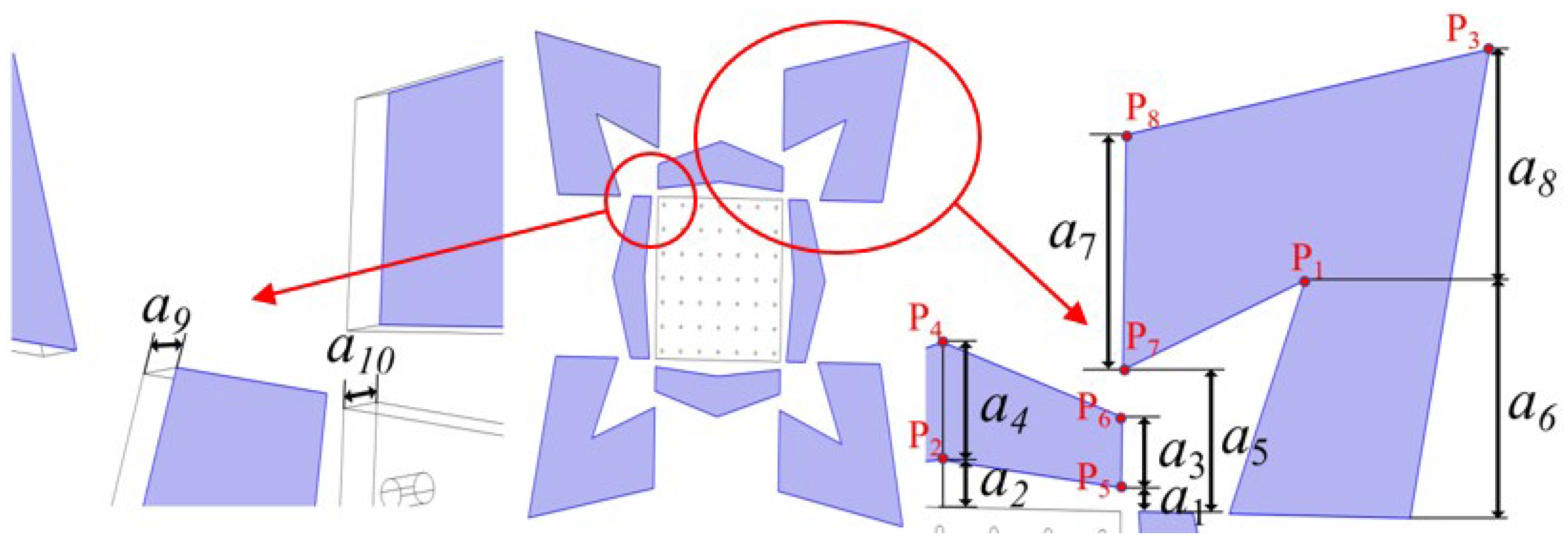
2.2. Geometric Model
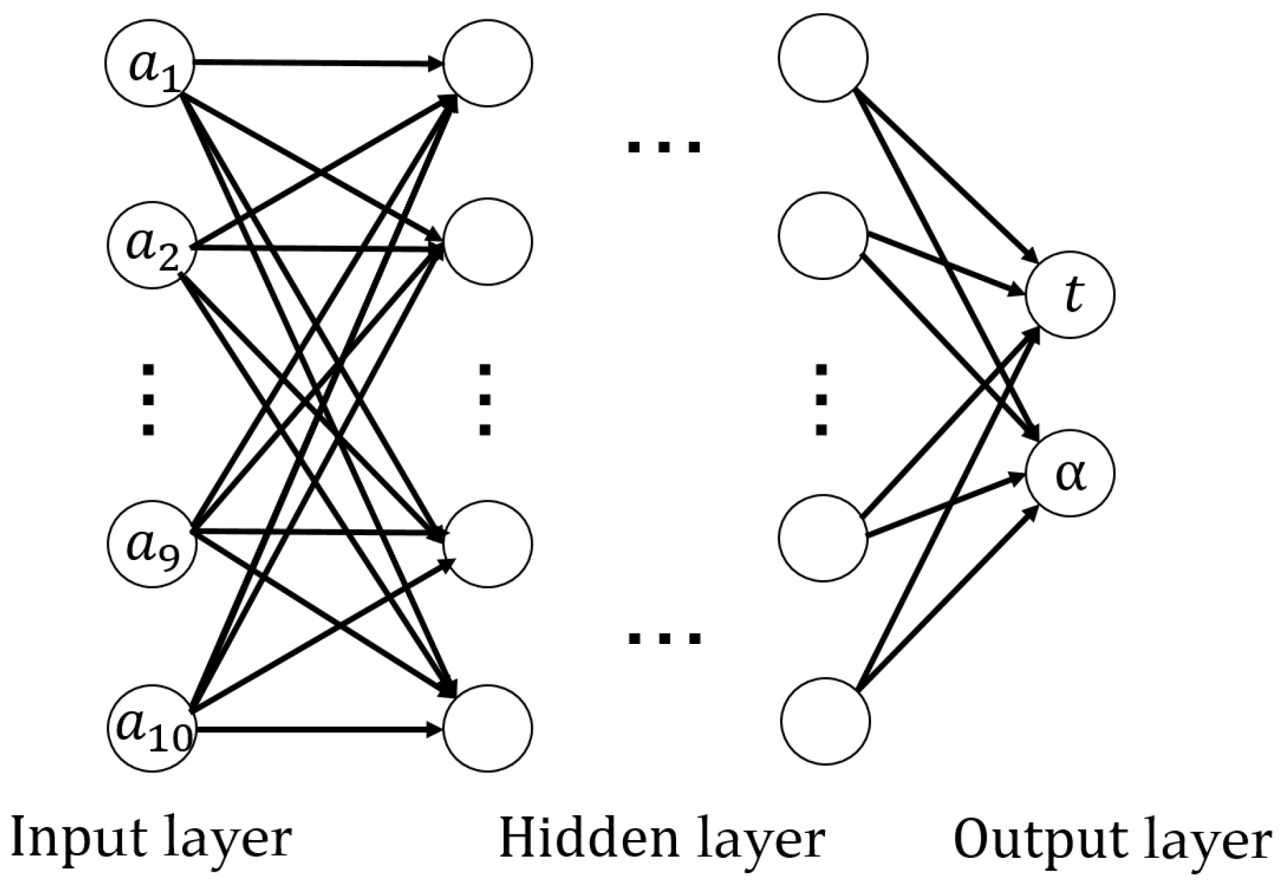
2.3. Establishment of Artificial Neural Networks
2.4. Multi-Objective Optimization
3. Results
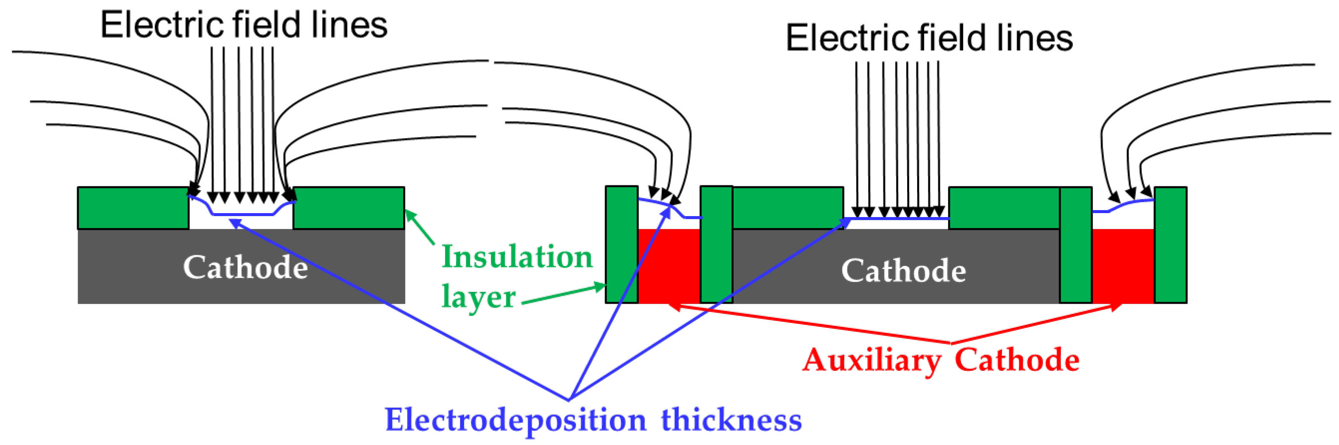
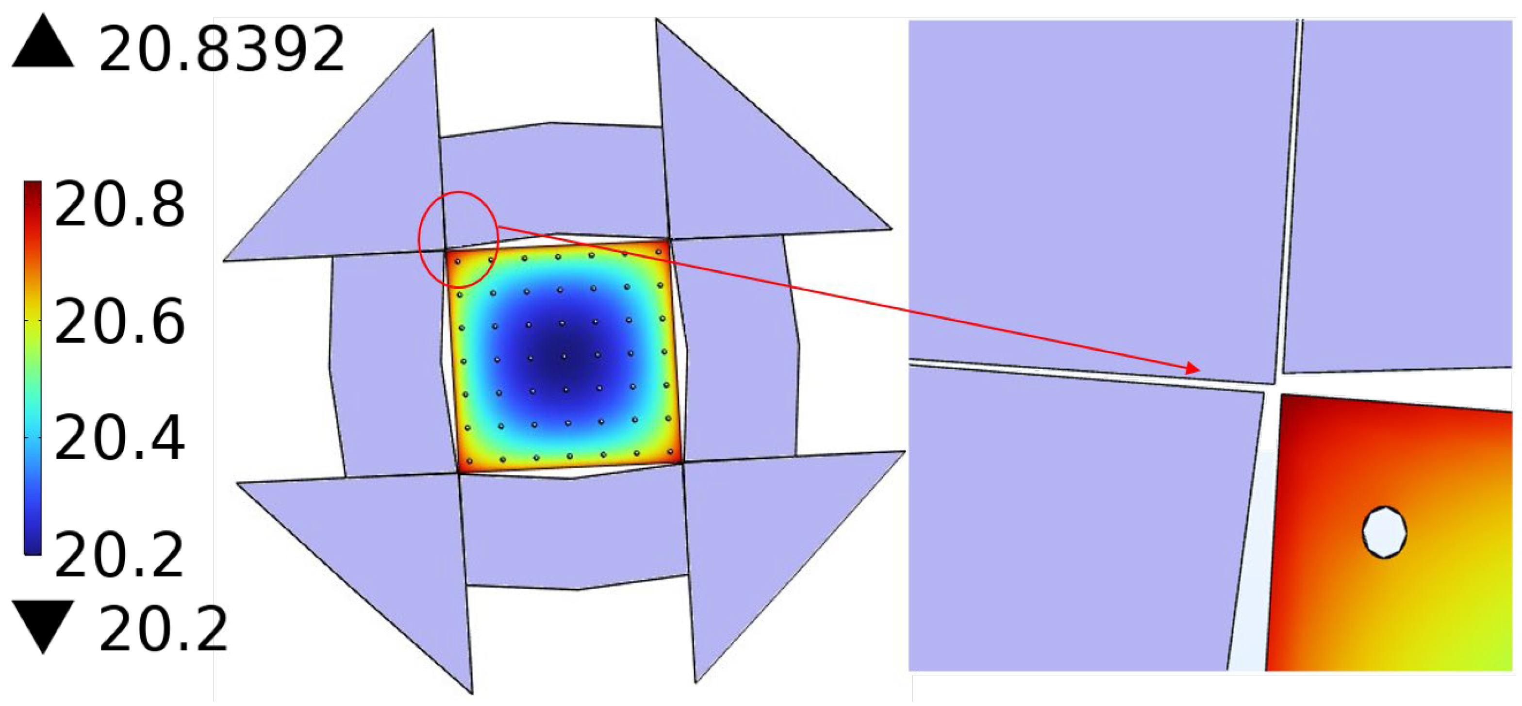
3.1. Effect of Auxiliary Cathode on Thickness Uniformity
3.2. Effect of Auxiliary Cathode Shape on Thickness Uniformity
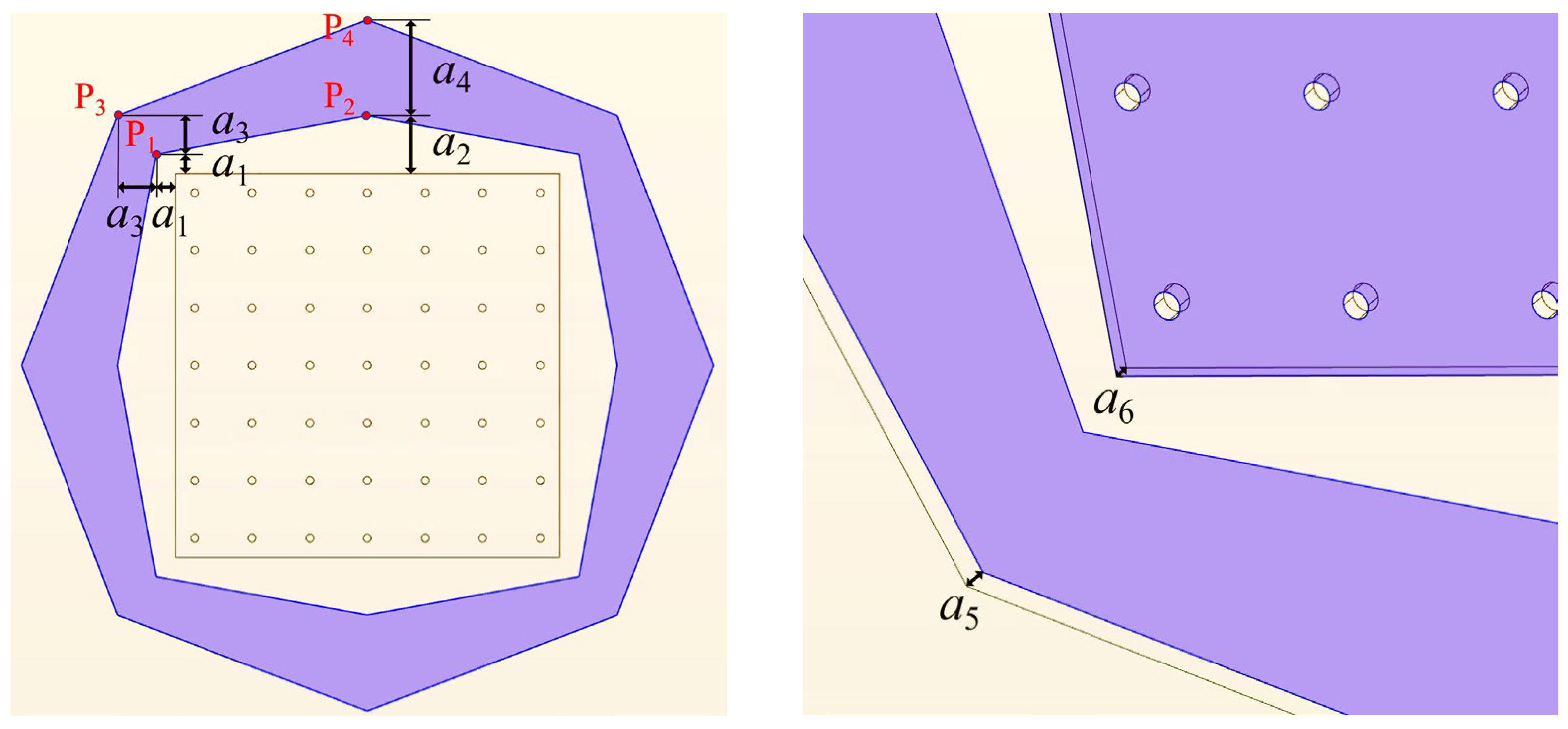
3.2.1. Optimization of Auxiliary Cathode Shape Parameters
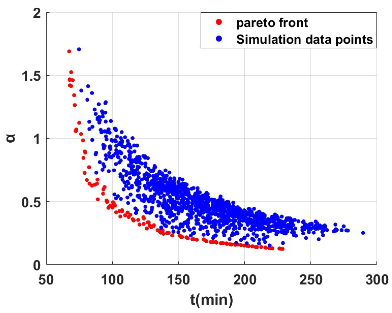
3.2.2. Multi-Objective Optimization Result
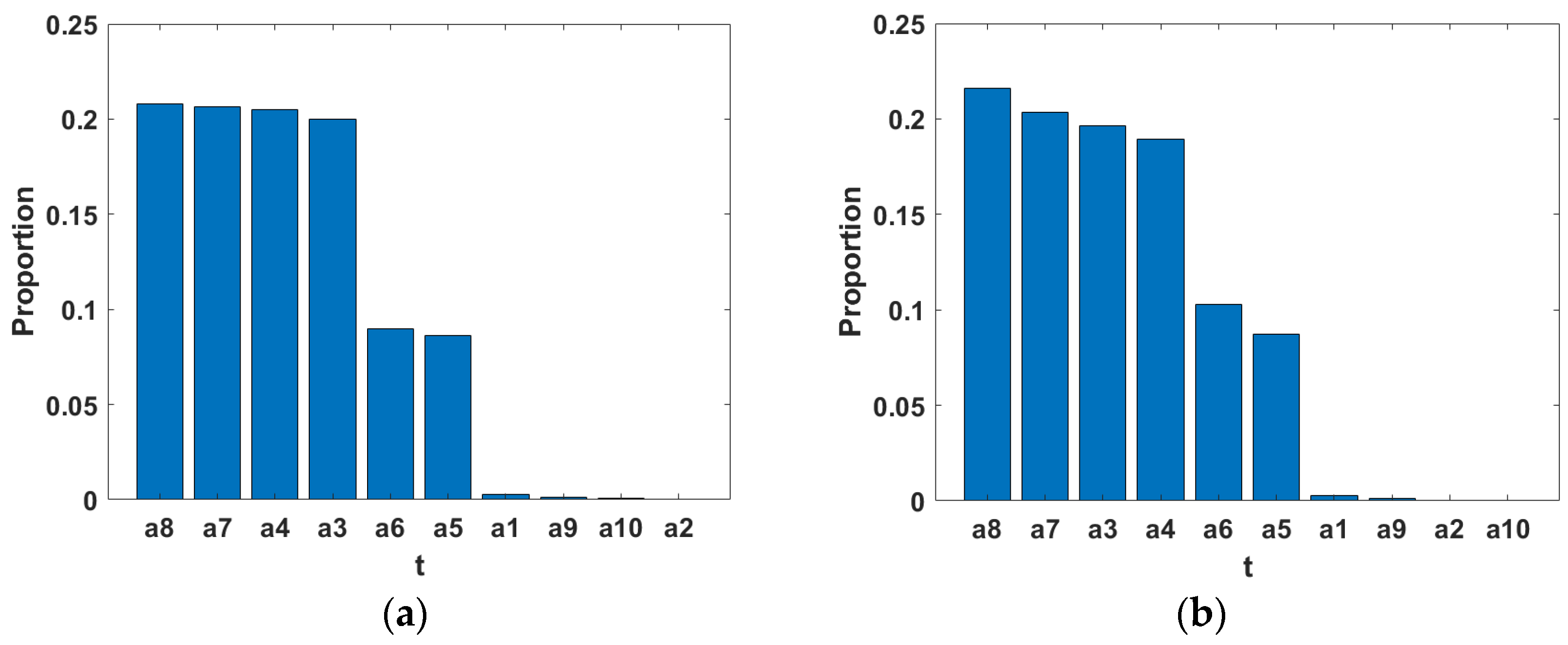
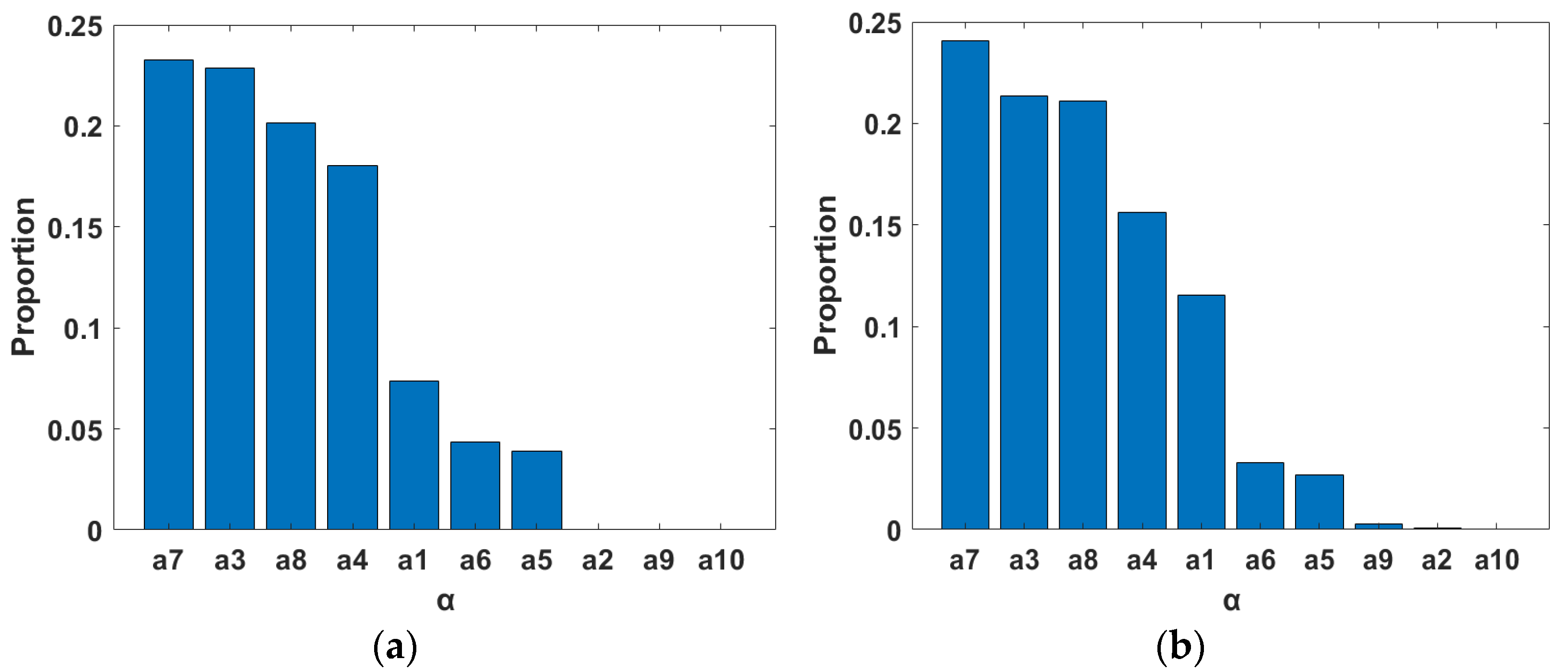
3.3. Parameter Importance
3.3.1. Electroforming Time
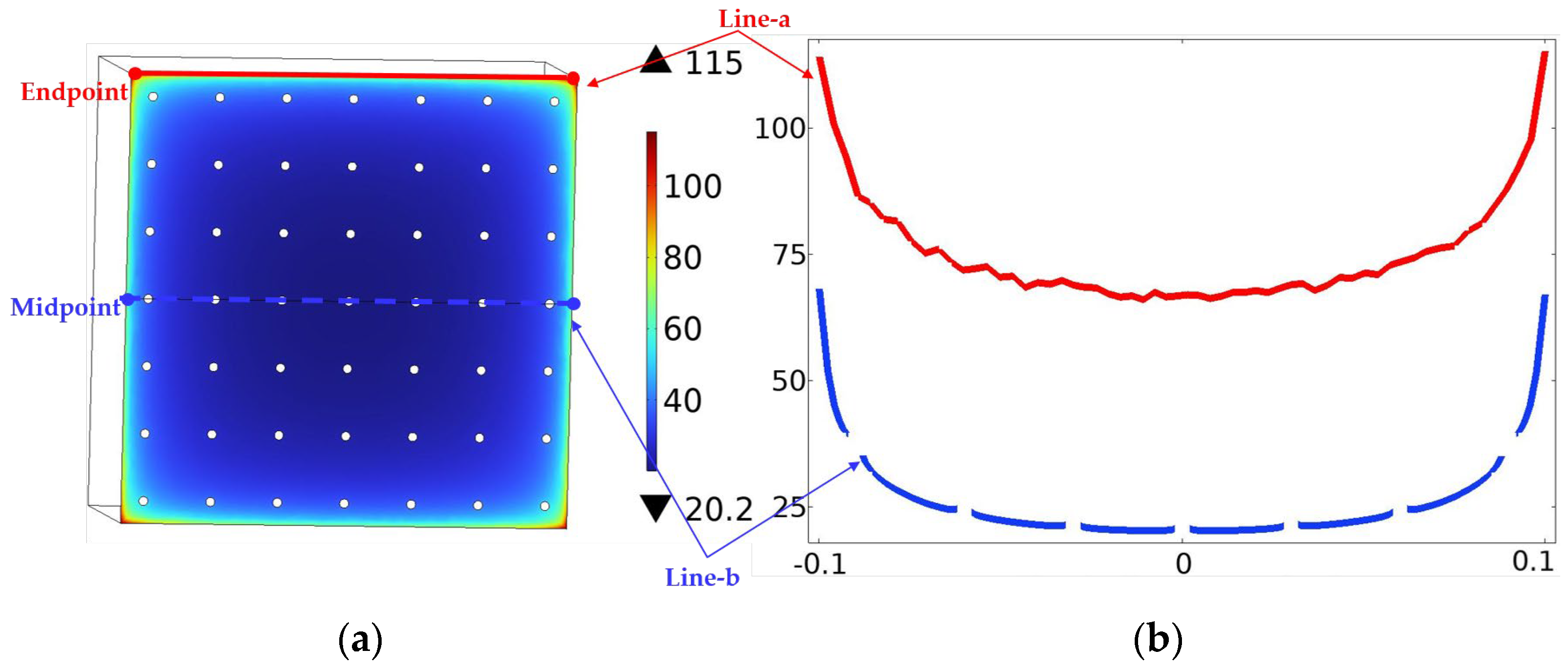
3.3.2. Thickness Uniformity
4. Conclusions
- In the case of fixed total current, the area of the auxiliary cathode is crucial for cathode uniformity; the larger the area, the better the thickness uniformity, while the influence of the shape parameter will be weakened.
- In the case of fixed average current density, the influence of the shape parameter is obvious, and the thickness uniformity can be further improved under a suitable shape parameter, but the optimization effect is still limited by the current density.
- The optimal auxiliary cathode parameter does not change with the change in average current density; it is not parallel to the cathode profile, but there is a certain angle.
- A method to find the shape of the auxiliary cathode is proposed, which can efficiently find the optimal auxiliary cathode parameters and shorten the electroforming time at the same time by establishing a neural network and multi-objective optimization.
Supplementary Materials
Author Contributions
Funding
Institutional Review Board Statement
Informed Consent Statement
Data Availability Statement
Conflicts of Interest
References
- Rai, P.K.; Gupta, A. Review—Electroforming Process for Microsystems Fabrication. J. Electrochem. Soc. 2023, 170, 123510. [Google Scholar] [CrossRef]
- Min, S.-K.; Lee, S.-N.; Kim, M.; Kim, K.-B. Development of Electroforming Technology for Flexible Metal Substrates for High-Efficiency Double-Sided Electronic Devices. Mater. Today Commun. 2024, 39, 108784. [Google Scholar] [CrossRef]
- Soergel, T. Innovative Battery Electrodes Via Composite Electroforming. ECS Meeting Abstr. 2022, MA2022-01, 2358. [Google Scholar] [CrossRef]
- Wu, K.; Ding, F.; Yang, Y.; Li, D.; Qiao, Z.; Qiang, P.; Wang, B. Influence on Imaging Performance and Evaluation of Wolter-I Type Mandrel Fabrication Errors. Appl. Opt. 2022, 61, 6617. [Google Scholar] [CrossRef] [PubMed]
- Yang, X.; Zhang, X.; Ming, P.; Li, Y.; Wang, W.; Zhang, Y.; Li, Z.; Li, L.; Xiao, Y.; Guo, X.; et al. Fabricating Ultra-Narrow Precision Slit Structures with Periodically Reducing Current Over-Growth Electroforming. Micromachines 2023, 15, 76. [Google Scholar] [CrossRef]
- Yanagishita, T.; Hidaka, T.; Suzuki, M.; Masuda, H. Polymer Lenses with Antireflection Structures Prepared Using Anodic Porous Alumina Molds. J. Vac. Sci. Technol. B Nanotechnol. Microelectron. Mater. Process. Meas. Phenom. 2016, 34, 021804. [Google Scholar] [CrossRef]
- Wang, L.; Jiao, L.; Pang, S.; Yan, P.; Wang, X.; Qiu, T. The Development of Design and Manufacture Techniques for Bioresorbable Coronary Artery Stents. Micromachines 2021, 12, 990. [Google Scholar] [CrossRef]
- Sun, H.; Wang, X.; Xiong, Y.; Liu, G.; Wang, K. Fabrication of Microlens Based on Overplating in Electroforming. J. Micromech. Microeng. 2016, 26, 055007. [Google Scholar] [CrossRef]
- Xu, L.; Liu, Y. A Microresonant Gas Sensor by Micro-Electroforming. J. Micro Nano-Manuf. 2015, 4, 014501. [Google Scholar] [CrossRef]
- Zhang, H.; Zhang, N.; Gilchrist, M.; Fang, F. Advances in Precision Micro/Nano-Electroforming: A State-of-the-Art Review. J. Micromech. Microeng. 2020, 30, 103002. [Google Scholar] [CrossRef]
- Chen, X.; Liu, L.; He, J.; Zuo, F.; Guo, Z. Fabrication of a Metal Micro Mold by Using Pulse Micro Electroforming. Micromachines 2018, 9, 203. [Google Scholar] [CrossRef]
- Qiang, L.; Weiping, L.; Huicong, L.; Liqun, Z. Fabrication of Nanostructured Electroforming Copper Layer by Means of an Ultrasonic-Assisted Mechanical Treatment. Chin. J. Aeronaut. 2010, 23, 599–603. [Google Scholar] [CrossRef]
- Wang, R.; Lv, H.; Zhai, J.; Shen, T. Research and Exploration of Terahertz Feeder Manufacturing Technology Based on Micro-Precision Machining. J. Phys. Conf. Ser. 2023, 2459, 012133. [Google Scholar] [CrossRef]
- Zhang, H.; Zhang, N.; Fang, F. Investigation of Mass Transfer inside Micro Structures and Its Effect on Replication Accuracy in Precision Microelectroforming. Int. J. Mach. Tools Manuf. 2021, 165, 103717. [Google Scholar] [CrossRef]
- Du, L.; Yang, T.; Zhao, M.; Tao, Y.; Luo, L.; Wang, L.; Liu, C. Study on Improving Thickness Uniformity of Microfluidic Chip Mold in the Electroforming Process. Micromachines 2016, 7, 7. [Google Scholar] [CrossRef]
- Xiang, J.; Chen, P.; Wang, Y.; Zeng, C.; Yang, W.; Li, J.; Xu, Y. Numerical Simulation of Optimizing Plating Uniformity of Interconnect Circuits on Printed Circuit Boards. J. Phys. Conf. Ser. 2021, 1986, 012135. [Google Scholar] [CrossRef]
- Wang, H.; Xing, J.; Fan, T.; Liu, J.; Xie, J.; Li, C. An Effect of Layered Auxiliary Cathode on Thickness Uniformity in Micro Electroforming Process. Micromachines 2023, 14, 1307. [Google Scholar] [CrossRef]
- Zhao, M.; Du, L.; Wei, Z.; Du, C.; Liu, X.; Ji, X. Fabrication of Metal Microfluidic Chip Mold with Coplanar Auxiliary Cathode in the Electroforming Process. J. Micromech. Microeng. 2018, 29, 025002. [Google Scholar] [CrossRef]
- Zhan, X.; Shen, C.; Zhu, Z.; Zhu, D. New Precision Electroforming Process for the Simultaneous Improvement of Thickness Uniformity and Microstructure Homogeneity of Wafer-Scale Nanotwinned Copper Arrays. Int. J. Mach. Tools Manuf. 2023, 187, 104006. [Google Scholar] [CrossRef]
- Wang, H.; Xie, J.; Fan, T.; Sun, D.; Li, C. Improving the Thickness Uniformity of Micro Gear by Multi-Step, Self-Aligned Lithography and Electroforming. Micromachines 2023, 14, 775. [Google Scholar] [CrossRef]
- Foukalas, F. A Survey of Artificial Neural Network Computing Systems. Cogn. Comput. 2024, 17, 4. [Google Scholar] [CrossRef]
- Ji, F.; Chen, C.; Zhao, Y.; Min, B. Optimization of Copper Electroforming Process Parameters Based on Double Hidden Layer BP Neural Network. Micromachines 2021, 12, 1157. [Google Scholar] [CrossRef] [PubMed]
- Sassi, W.; Mrad, M.; Behera, D.; Ammar, S.; Hihn, J.Y. Prediction and Optimization of Electroplated Ni-Based Coating Composition and Thickness Using Central Composite Design and Artificial Neural Network. J. Appl. Electrochem. 2021, 51, 1591–1604. [Google Scholar] [CrossRef]
- Subramanian, K.; Periasamy, V.M.; Pushpavanam, M.; Ramasamy, K. Predictive Modeling of Deposition Rate in Electro-Deposition of Copper–Tin Using Regression and Artificial Neural Network. J. Electroanal. Chem. 2009, 636, 30–35. [Google Scholar] [CrossRef]
- Haghdoost, A.; Pitchumani, R. Numerical Analysis of Electrodeposition in Microcavities. Electrochim. Acta 2011, 56, 8260–8271. [Google Scholar] [CrossRef]
- Jiang, B.; Weng, C.; Zhou, M.; Lv, H.; Drummer, D. Improvement of Thickness Deposition Uniformity in Nickel Electroforming for Micro Mold Inserts. J. Cent. South Univ. 2016, 23, 2536–2541. [Google Scholar] [CrossRef]


(S/m) | (A) | (K) | (V) | (kg/mol) | (kg/m3) | n | ||||
|---|---|---|---|---|---|---|---|---|---|---|
| 0.95 | 9 × 10⁻⁴ | 1.5 | 0.5 | 333.15 | −0.257 | 0.0586 | 8900 | 1 | 2 | 0.1 |
| Parameter | Definition | Value Range |
|---|---|---|
| a1 | Perpendicular distance from diagonal endpoints (P1) to cathode | 1 × 10⁻⁵~1 × 10⁻³ |
| a2 | Perpendicular distance from perpendicular endpoints (P2) to cathode boundary | 1 × 10⁻⁵~1 × 10⁻³ |
| a3 | Additional offset extending from a1 on the opposite | 1 × 10⁻⁵~1 × 10⁻³ |
| a4 | Additional offset extending from a2 on the opposite side | 1 × 10⁻⁵~1 × 10⁻³ |
| a5 | Height difference between auxiliary cathode and cathode surface | 1 × 10⁻⁶~5 × 10⁻⁵ |
| a6 | Thickness of the photoresist (non-conductive layer) | 2 × 10⁻⁵~5 × 10⁻⁵ |
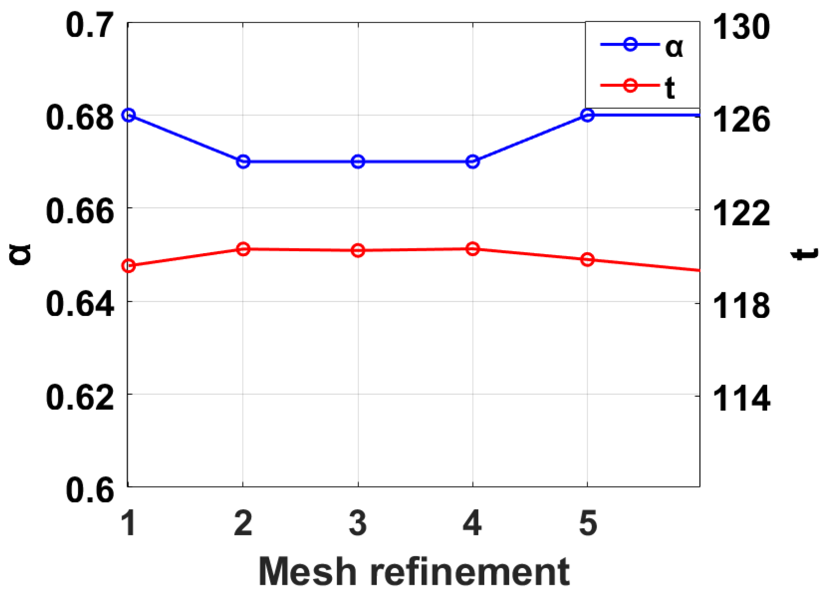
| Maximum Element Size (cm) | α | t (Min) |
|---|---|---|
| 0.144 | 0.68 | 119.6 |
| 0.072 | 0.67 | 120.32 |
| 0.036 | 0.67 | 1206 |
| 0.018 | 0.67 | 120.33 |
| 0.009 | 0.68 | 119.87 |
| 0.0045 | 0.68 | 119.39 |
| Maximum Element Size (cm) | Minimum Element Size (cm) | Maximum Element Growth Rate | Curvature Factor | Narrow Region Resolution |
|---|---|---|---|---|
| 0.018 | 0.0006 | 1.3 | 0.2 | 1 |
| a1 (m) | a2 (m) | a3 (m) | a4 (m) | a5 (m) | a6 (m) | t (min) | α |
|---|---|---|---|---|---|---|---|
| 1 × 10⁻⁵ | 1 × 10⁻⁵ | 1 × 10⁻³ | 1 × 10⁻³ | 5 × 10⁻⁵ | 5 × 10⁻⁵ | 227 | 0.12 |
| Parameter | Definition | Value Range |
|---|---|---|
| a1 | Perpendicular distance from the right-angle edge endpoint P5 to the cathode boundary | 1 × 10⁻⁵~1 × 10⁻³ |
| a2 | Perpendicular distance from perpendicular endpoints (P2) to cathode boundary | 1 × 10⁻⁵~1 × 10⁻³ |
| a3 | Additional offset from a1 at endpoint P5, extending toward the opposite boundary | 1 × 10⁻⁵~1 × 10⁻³ |
| a4 | Additional offset extending from a2 on the opposite side | 1 × 10⁻⁵~1 × 10⁻³ |
| a5 | Perpendicular distance from the right-angle edge endpoint P7 to the cathode boundary | 1 × 10⁻⁵~1 × 10⁻³ |
| a6 | Perpendicular distance from diagonal endpoints (P1) to cathode | (1 × 10⁻⁵)/~1 × 10−3 |
| a7 | Additional offset from a1 at endpoint P7, extending toward the opposite boundary | 1 × 10⁻⁵~1 × 10⁻³ |
| a8 | Additional offset extending from a6 on the opposite | (1 × 10⁻⁵)/~1 × 10−3 |
| a9 | Height difference between auxiliary cathode and cathode surface | 1 × 10⁻⁶~5 × 10⁻⁵ |
| a10 | Thickness of the photoresist (non-conductive layer) | 2 × 10⁻⁵~5 × 10⁻⁵ |
| a1 | a2 | a3 | a4 | a5 | a6 | a7 | a8 | a9 | a10 | α | |
|---|---|---|---|---|---|---|---|---|---|---|---|
| 55.97 A/m2 | 1.61 × 10⁻⁵ | 1.06 × 10⁻⁴ | 1 × 10⁻³ | 1 × 10⁻³ | 1 × 10⁻³ | (1 × 10⁻⁵) / | 1 × 10⁻³ | 1 × 10⁻³ | 5 × 10⁻⁵ | 5 × 10⁻⁵ | 0.04 |
| 200 A/m2 | 1.61 × 10⁻⁵ | 1.06 × 10⁻⁴ | 1 × 10⁻³ | 1 × 10⁻³ | 1 × 10⁻³ | (1 × 10⁻⁵) / | 1 × 10⁻³ | 1 × 10⁻³ | 5 × 10⁻⁵ | 5 × 10⁻⁵ | 0.10 |
Disclaimer/Publisher’s Note: The statements, opinions and data contained in all publications are solely those of the individual author(s) and contributor(s) and not of MDPI and/or the editor(s). MDPI and/or the editor(s) disclaim responsibility for any injury to people or property resulting from any ideas, methods, instructions or products referred to in the content. |
© 2025 by the authors. Licensee MDPI, Basel, Switzerland. This article is an open access article distributed under the terms and conditions of the Creative Commons Attribution (CC BY) license (https://creativecommons.org/licenses/by/4.0/).
Share and Cite
Chen, C.; Liu, S.; Zhao, M.; Zhou, J.; Song, K.; Liu, J. Machine Learning Optimization of Auxiliary Cathode Structure for Thickness Uniformity in Micro-Electroforming. Coatings 2025, 15, 652. https://doi.org/10.3390/coatings15060652
Chen C, Liu S, Zhao M, Zhou J, Song K, Liu J. Machine Learning Optimization of Auxiliary Cathode Structure for Thickness Uniformity in Micro-Electroforming. Coatings. 2025; 15(6):652. https://doi.org/10.3390/coatings15060652
Chicago/Turabian StyleChen, Chen, Shuli Liu, Min Zhao, Jiajie Zhou, Kui Song, and Jingang Liu. 2025. "Machine Learning Optimization of Auxiliary Cathode Structure for Thickness Uniformity in Micro-Electroforming" Coatings 15, no. 6: 652. https://doi.org/10.3390/coatings15060652
APA StyleChen, C., Liu, S., Zhao, M., Zhou, J., Song, K., & Liu, J. (2025). Machine Learning Optimization of Auxiliary Cathode Structure for Thickness Uniformity in Micro-Electroforming. Coatings, 15(6), 652. https://doi.org/10.3390/coatings15060652