Abstract
This study provides a comprehensive investigation into the growth behavior of boron nitride (BN) buffer layers on Silicon carbide (SiC) substrates and their influence on interfacial band alignment. BN layers were deposited on semi-insulating SiC by RF magnetron sputtering with deposition times of 2.5, 5, and 7.5 min (these deposition times are specific experimental parameters to adjust the thickness of the amorphous BN layer, not intrinsic material properties of BN). Atomic force microscopy revealed that the surface roughness of the BN layers initially decreased and then increased with thickness, indicating an evolution from nucleation to continuous film formation, followed by surface coarsening. Transmission electron microscopy confirmed the BN thicknesses of approximately 3.25, 4.91, and 7.57 nm, showing that the layers gradually became uniform and compact, thereby improving the structural integrity of the BN/SiC interface. Band alignment was analyzed using the Kraut method, yielding a valence band offset of ~0.36 eV and a conduction band offset of ~2.34 eV for the BN/SiC heterojunction. This alignment indicates that the BN buffer layer introduces a pronounced electron barrier, effectively suppressing leakage, while the relatively small VBO facilitates hole transport across the interface. These findings demonstrate that the BN buffer layer enhances interfacial bonding, reduces defect states, and enables band structure engineering, offering a promising strategy for improving the performance of wide-bandgap semiconductor devices.
1. Introduction
Semi-insulating 4H-Silicon carbide (4H-SiC), a representative third-generation wide-bandgap semiconductor material, has attracted considerable attention for power and optoelectronic device applications owing to its wide bandgap of ~3.2 eV, high critical electric field of ~3 MV·cm−1 [1,2,3], and outstanding thermal conductivity and thermal stability. Nevertheless, the performance of 4H-SiC-based devices is often constrained by interfacial states and structural defects, which reduce carrier mobility, increase channel resistance, and compromise device reliability [4,5,6]. Consequently, interface engineering aimed at improving the quality of the 4H-SiC/buffer or passivation layer interface has emerged as a key strategy to enhance device performance [7,8,9,10].
Amorphous boron nitride (a-BN), a layered material with a wide bandgap of ~5.9 eV [11,12], exhibits excellent thermal stability and chemical inertness, rendering it a promising candidate for wide-bandgap semiconductor heterostructures [13,14]. Previous studies have demonstrated that BN films, when employed as buffer layers, can significantly improve interface quality, suppress defect states, and modulate band alignment [12,15,16]. To clarify “surface defect states”, we refer here to point defects and local bonding disorders at the interface (e.g., vacancies, dangling bonds, F-centers, and pit/step features on SiC surfaces), which can introduce midgap states and promote carrier trapping or band bending [5,17], thereby optimizing the Schottky barrier height and electrical properties of devices. In particular, BN interlayers are expected to serve as effective interface modulation layers in wide-bandgap semiconductors such as SiC, enhancing both the power-handling capability and long-term stability of devices [18,19].
Although several studies have reported the growth of BN on SiC surfaces and the basic properties of BN/SiC heterostructures [15,20], systematic investigations of the effect of BN thickness on the interfacial structure and band alignment remain limited. Herein, BN films with different deposition times (2.5, 5, and 7.5 min) were deposited on SiC substrates by magnetron sputtering. Their surface morphology, interfacial structure, and chemical states were comprehensively characterized using Atomic force microscopy (AFM), Transmission electron microscopy (TEM), and X-ray photoelectron spectroscopy (XPS). Furthermore, the band alignment of BN/SiC heterojunctions was determined using the Kraut method, elucidating the influence of BN thickness on the valence band offset (ΔEV) and conduction band offset (ΔEC). These findings provide both experimental evidence and theoretical insights into the role of BN buffer layers in the interface engineering of SiC-based systems.
2. Experimental Procedure
2.1. Sample Preparation
The semi-insulating SiC substrates were used in this study. Prior to deposition, their surfaces were ultrasonically cleaned in organic solvents and rinsed with deionized water to remove contaminants. BN films were deposited by magnetron sputtering using a high-purity BN target. In the sputtering process, the RF power was set to 150 W, the chamber pressure was stabilized at 1 Pa, and the substrate temperature was maintained at ~200 °C. A mixed Ar/N2 atmosphere with a flow ratio of 30:10 was employed, and the target was pre-sputtered for 20 min to eliminate surface impurities and stabilize the plasma environment. Film thickness was tuned by varying the deposition time to 2.5, 5, and 7.5 min under identical conditions, ensuring that thickness was the only variable. A sample with 0 min deposition (bare SiC substrate) served as the control to evaluate the influence of BN insertion on the interfacial structure and band alignment. After deposition, all samples were immediately transferred and stored in a clean environment to minimize contamination before characterization.
2.2. Characterization Methods
The samples were characterized in terms of morphology, structure, and electronic properties. The surface morphology of the SiC substrates and BN films with different deposition times was examined using anAFM (Dimension ICON, Bruker, Billerica, MA, USA), providing two-dimensional (2D) and three-dimensional (3D) images along with height distribution profiles; all AFM images were acquired over 5 × 5 μm2 scan areas. For each sample, three independent regions were randomly selected and measured. The reported surface roughness values are given as the mean ± sample standard deviation (mean ± SD) of these three measurements. Surface roughness and related parameters were extracted to quantitatively analyze the influence of BN thickness on morphological evolution. Cross-sectional observations were obtained using TEM (Talos F200X, Thermo Fisher Scientific, Waltham, MA, USA) to evaluate film continuity, interface features, and thickness. Furthermore, TEM specimens were prepared usingdual-beam focused ion beam (FIB) system (Helios 5 CX, Thermo Fisher Scientific, Waltham, MA, USA) to ensure clear visualization of the interface. Chemical composition and bonding states were investigated by XPS (AXIS Supra+, Shimadzu, Kyoto, Japan) with a monochromatic Al Kα source (1486 eV). Survey scans were acquired with a step size of 1 eV, while high-resolution scans were recorded with a step size of 0.05 eV. Surface contamination resulted in a C 1 peak at 284.8 eV, which was used for charge correction, while 5 keV Ar+ ion sputtering provided depth profiling, a setting optimized for efficient removal of surface contamination and for depth profiling in our instrument. XPS data were employed to analyze the composition and bonding of BN films, as well as the band alignment of the BN/SiC heterojunction. The peak value of the valence band was determined through linear extrapolation of the valence band spectrum, and band offsets were calculated using the Kraut method.
3. Results and Discussion
3.1. Analysis of Surface Morphology and Structural Characteristics
Figure 1a presents the AFM-based characterization of the SiC substrate before BN deposition, including 2D surface morphology, 3D topography, and height profiles [21]. The SiC surface appears smooth overall, exhibiting only a few uniformly distributed step-like features and shallow grooves, which originate from the intrinsic steps of the SiC crystal and residual polishing effects [22,23]. The 3D topography further reveals minimal surface undulation, with an absence of large particles or island-like features, confirming the flatness and uniformity of the substrate.
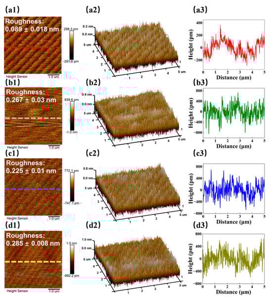
Figure 1.
AFM images of the SiC substrate and BN films grown for different deposition times, showing surface morphology, 3D topography, and height profiles: (a) bare SiC substrate; BN films deposited for (b) 2.5 min, (c) 5 min, (d) 7.5 min.
Height profiles reveal that surface variations are primarily confined to the nanometer scale and change gradually, with a surface roughness of 0.089 ± 0.018 nm, representing an exceptionally smooth surface. This highly smooth surface provides favorable conditions for subsequent BN nucleation and epitaxial growth, facilitating the formation of uniform and continuous thin films.
Compared with the bare SiC substrate, the BN film deposited for 2.5 min exhibits significant changes in surface morphology (Figure 1b). The 2D AFM image shows numerous uniformly distributed granular structures [24,25,26], indicating that BN nucleates in an island-like form on the SiC surface during the initial deposition stage. The 3D topography further reveals height variations among these granular features, resulting in an overall increase in surface undulation. Height profile analysis indicates that the surface roughness has increased notably compared with the bare substrate, reaching 0.267 ± 0.03 nm, with more pronounced peak-to-valley variations. These observations suggest that, at the early stage, the BN film only but exists as dispersed islands. The morphology is consistent with a typical “nucleation–island growth” mode, in which BN preferentially nucleates at regions of lower local energy or surface defects and gradually expands to form larger, interconnected domains. This early-stage island structure establishes the foundation for the subsequent formation of a continuous BN film.
Furthermore, Figure 1c depicts the surface morphology of the BN film after 5 min of deposition. The 2D AFM image shows that the gaps between surface particles have decreased [27], and the film exhibits higher coverage, indicating the partial growth and coalescence of the islands. The 3D topography clearly demonstrates a transition from the initially isolated islands to a more continuous film, accomplished by reduced surface undulation compared to the 2.5 min sample. Furthermore, height profile analysis reveals a reduction in surface roughness to 0.225 ± 0.01 nm, with peak-to-valley variations becoming more moderate, indicating a denser surface. Based on nucleation and growth mechanisms, extended deposition drives the BN film from the “island nucleation stage” to the “island coalescence” stage, promoting continuous coverage by the lateral growth and merging of particles. At this stage, enhanced surface flatness facilitates interface formation and enables subsequent band alignment studies.
The surface morphology of the BN film further evolved after the deposition time was extended to 7.5 min (Figure 1d). The 2D AFM image shows that the film has achieved near-complete coverage, with no exposed substrate areas and overall uniform morphology [28]. However, compared with the 5 min sample, localized regions exhibit larger protrusions, suggesting additional particle accumulation or secondary nucleation following continuous layer formation. The 3D topography reveals increased surface undulation relative to the 5 min sample, demonstrating that excessive deposition induced local roughness. This observation is further confirmed by height profile analysis, showing more pronounced peak-to-valley variations and an increase in surface roughness to 0.285 ± 0.008 nm. Based on growth mechanisms, the BN film at 7.5 min enters an “overgrowth” stage. Although the layer is continuous, atomic diffusion and local secondary nucleation lead to a rebound in roughness. This evolution indicates that the optimal surface flatness is achieved at intermediate deposition time (~5 min), whereas excessive deposition results in increased roughness.
Furthermore, Figure 2 presents cross-sectional TEM images of the SiC substrate and BN films deposited on the substrate for different durations [22,29,30]. The bare SiC substrate (Figure 2a) displays a dense crystalline structure with well-defined layers, confirming good crystallinity and surface flatness prior to deposition. In contrast, Figure 2b–d show the cross-sectional morphologies of BN films sputtered on SiC for 2.5, 5, and 7.5 min, respectively.
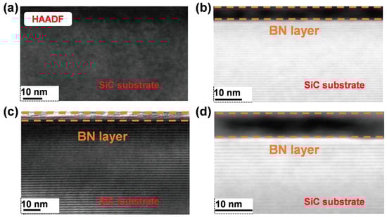
Figure 2.
Cross-sectional TEM images of the BN films deposited on the SiC substrate for different growth times: (a) 0 min (bare SiC), (b) 2.5 min, (c) 5 min, and (d) 7.5 min.
From the TEM analysis, the thicknesses of BN layers at different deposition times are 3.25 nm, 4.91 nm, and 7.57 nm, respectively. These thickness values were extracted from representative cross-sectional TEM images and may have an uncertainty of approximately 0.2-0.3 nm. At 2.5 min (Figure 2b), the BN layer exhibits local discontinuities and non-uniform thickness [31,32], forming island-like thickened regions, consistent with the higher surface roughness observed using AFM. Prolonging the deposition time to 5 min (Figure 2c) produces a thicker and more continuous BN layer with a relatively flat interface, indicating the merging of nucleated islands into a dense coverage. Furthermore, complete coverage of the BN layer is observed at 7.5 min (Figure 2d), although localized thickness variations and protrusions indicate secondary nucleation or overgrowth following continuous film formation. These results align with the increase in the roughness measured by AFM. Based on these results, the estimated deposition rates are ~1.25, 0.99, and 1.02 nm·min−1 for 2.5, 5, and 7.5 min, respectively, with an average rate of ~1.09 nm·min−1. This indicates that under identical sputtering conditions, the BN film grows at a generally stable rate of ~1 nm·min−1. Overall, the interface remains dense and well-bonded, demonstrating the stable deposition characteristics of BN on SiC under the applied magnetron sputtering conditions.
3.2. Study of Band Alignment in BN/SiC Heterojunctions
In wide-bandgap semiconductor heterostructures, the band alignment directly governs carrier transport across the interface, ultimately affecting device performance [5,33,34]. The ΔEV and ΔEC govern the interfacial charge distribution and barrier height, also determining key device parameters such as the Schottky barrier height [35,36], breakdown voltage, and photodetection range. For SiC-based devices, performance is often constrained by carrier scattering and recombination losses, arising from interface states and band misalignment. Therefore, the introduction of an appropriate buffer layer and its precise tuning offers a promising approach to optimize the band alignment at the BN/SiC interface, thereby enhancing both electrical and optoelectronic properties.
Additionally, the synthesized materials were analyzed using XPS. Figure 3 presents the XPS results of BN films deposited on SiC substrates [37,38], including the survey spectrum, valence band spectrum, and high-resolution core-level spectra. In the survey spectrum (Figure 3a), distinct B 1s and N 1s peaks are observed, indicating the film is composed mainly of boron nitride. Slight surface oxidation or environmental contamination leads to weak O 1s and C 1s signals.

Figure 3.
XPS characterization of boron nitride: (a) survey spectrum, (b) valence band spectrum, and high-resolution core-level spectra for (c) N 1s and (d) B 1s.
The valence band spectrum (Figure 3b) shows a valence band maximum (VBM) of 2.68 ± 0.05 eV with respect to the Fermi level, determined by linear extrapolation, the uncertainty in VBM determination, including fitting residuals and instrument resolution, is estimated at ±0.05 eV, consistent with the wide-bandgap nature of BN and providing essential parameters for subsequent band alignment analysis. The high-resolution N 1s spectrum (Figure 3c) can be deconvoluted into three components. A main peak at 398.57 eV corresponding to N-B bonds, accounting for ~81.6% of the signal and indicating that the BN film is predominantly composed of B-N bonds. Furthermore, a shoulder at 400.20 eV (~15.2%) attributed to N-C bonds, possibly originating from the substrate or residual contamination. Another minor component at 401.84 eV (~3.2%) is assigned to N-O bonds, arising likely due to slight surface oxidation. Similarly, the high-resolution B 1s spectrum (Figure 3d) exhibits clear peak splitting. The main peak at 190.42 eV corresponds to B-N bonds (~81.9%), confirming the dominant B-N composition of the film. The two minor components are also observed at 188.90 eV (B-C, ~13.8%) and 191.55 eV (B-O, ~4.3%), indicating the presence of trace impurity bonds or surface oxidation.
XPS analysis of the BN films indicates that the predominant bonding is B-N, with minor contributions from B-C, N-C, and oxidation-related B-O and N-O bonds. The small amounts of carbon- and oxygen-related bonds likely arise from interactions with the substrate or the environment during film growth; however, their overall content is low and does not affect the intrinsic properties of the boron nitride film. Previous studies report reference values for SiC substrates, supplying essential energy-level information, including the valence band maximum, which is critical for investigating the band alignment in BN/SiC heterojunctions, as summarized in Table 1.

Table 1.
Bandgap, valence band maximum (VBM), core-level binding energies, and the energy difference between the core levels and the corresponding VBM energy in BN and SiC samples.
Additionally, the synthesized BN/SiC interface was examined by XPS (Figure 4). The high-resolution core-level spectra and peak deconvolution reveal the chemical bonding and interfacial interaction mechanisms [39].
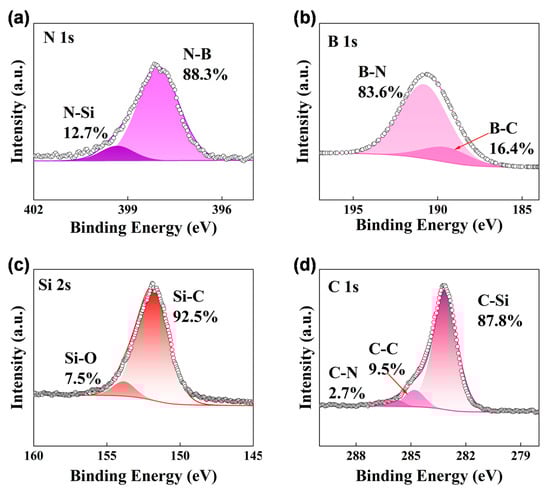
Figure 4.
High-resolution peak deconvolution of the BN/SiC interface: (a) N 1s, (b) B 1s, (c) Si 2s, and (d) C 1s.
In the N 1s spectrum, the dominant peak at 398.03 eV corresponds to N-B bonds (88.3%), indicating the predominant bonding between nitrogen atoms and boron at the interface, thereby preserving the primary BN structure. A shoulder at 399.34 eV is attributed to N-Si bonds (~12.7%), suggesting a certain degree of chemical interaction between BN and the SiC substrate through bonding between nitrogen and silicon. In the B 1s spectrum, the main peak at 190.80 eV corresponds to B-N bonds (83.6%), confirming the predominant presence of BN bonding at the interface. A minor component at 189.50 eV (~16.4%) is attributed to B-C bonds, indicating the possibility of bonding between boron atoms and carbon atoms on the SiC surface. In the Si 2s spectrum, the principal peak at 151.89 eV is assigned to Si-C bonds (~92.5%), representing the primary SiC lattice structure, while a minor peak at 153.85 eV (~7.5%) corresponds to Si-O bonds, likely arising from slight oxidation at the interface or surface. In the C 1s spectrum, the primary peak at 283.13 eV corresponds to C-Si bonds (~87.8%), consistent with the SiC lattice, while additional peaks at 284.80 eV (C-C, ~9.5%) and 285.68 eV (C-N, ~2.7%) are also observed. The C-C peak originates from minor surface contamination, whereas the presence of C-N bonds indicates partial chemical interactions between carbon atoms and nitrogen in the BN film, providing further insight into interfacial reactions. The interfacial chemical species we observe (B-C, N-Si and minor Si-O) are consistent with localized chemical interactions that likely coexist with defect states and influence the electronic structure. Further work, including targeted defect spectroscopy and electrical characterization (e.g., EPR, DLTS, STM/STS), is needed to quantify their roles for device performance [5,17]. And the weak Si-O signal detected by XPS suggests the potential presence of an extremely thin oxide layer at the interface. Although its impact on band shifts is limited, this interfacial layer may introduce minor deviations, necessitating more systematic verification in subsequent studies using methods such as TEM-EELS or XRR. Additionally, in future experiments we will include low-energy sputter tests, angle-resolved XPS (ARXPS) and complementary techniques such as AES or Raman spectroscopy to further validate the chemical assignments.
Overall, the XPS peak deconvolution of the BN/SiC interface reveals distinct chemical interactions. The BN film retains a stable structure dominated by B-N and Si-C bonds. Conversely, the detection of N-Si, B-C, and C-N bonds indicates localized chemical reactions occurring at the interface. These bonding features suggest the formation of strong interfacial coupling between BN and SiC, enhancing adhesion, modulating dipoles and band offsets at the interface, and thereby providing essential information for subsequent band alignment calculations.
As shown in Figure 5, the measured binding energies of N 1s and Si 2s are 398.03 eV and 151.89 eV, respectively, resulting in a core-level energy difference (ΔECL) of 246.14 eV.
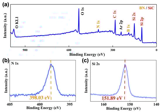
Figure 5.
BN/SiC interface: (a) XPS survey spectrum, and high-resolution core-level spectra for (b) N 1s, and (c) Si 2s.
According to the Kraut method, the ΔEV of the BN/SiC heterojunction is determined by analyzing the difference in energy between VBM and the corresponding core levels (ECL), as described below [40,41,42,43]:
In Equation (1), the first and second terms represent the energy differences between the core levels and the VBM of the BN film and the SiC substrate, respectively. Furthermore, in Equation (2), ΔECL corresponds to the difference in energy between the core levels of BN and SiC at the heterojunction interface. Using the measured values of ΔEg and ΔEV, the CBO ( at the BN/SiC interface is calculated according to Equation (3):
represent the bandgaps of the SiC substrate and the BN film at room temperature, respectively. The calculated ΔEV is −0.36 ± 0.08 eV, and the ΔEC is −2.34 ± 0.10 eV [41,43]. The uncertainties were derived from error propagation of VBM fitting, core-level fitting, charging correction, and bandgap variability. To verify the reliability of the present results, a comparative analysis was conducted by correlating with the density functional theory (DFT) simulation study reported by Bo et al. [16]. In their work, the CASTEP software combined with the HSE06 hybrid functional was employed to construct van der Waals (vdW) heterojunction models of BN/SiC with lattice strains of 7.37% and 5.93%, respectively. The calculated band gaps for these two models were 0.851 eV and 1.373 eV, which revealed a clear trend that “an increase in lattice strain leads to a decrease in band gap”. This conclusion is in good agreement with the experimental phenomena observed in this study.
Figure 6 presents a schematic of the BN/SiC heterojunction band alignment, calculated using the Kraut method. The results indicate that the VBM and CBM of BN are shifted by ~0.36 eV and ~2.34 eV, respectively, relative to SiC. This band alignment corresponds to a type-I heterojunction, with a large CBO forming a significant barrier to electron transport, while the VBO is comparatively small. For devices, the substantial CBO (~2.34 eV) effectively suppresses electron leakage at the interface and minimizes interfacial recombination, thereby enhancing breakdown voltage and overall stability. Meanwhile, the modest VBO (~0.36 eV) presents a low barrier to hole transport at the interface. This asymmetric band offset is advantageous for optimizing carrier distribution and regulating interfacial charge transport, making the BN layer a key functional component for enhancing the performance of SiC-based power and optoelectronic devices.
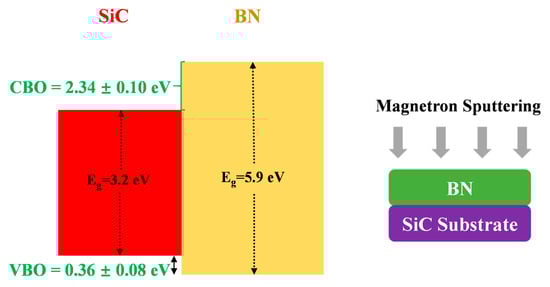
Figure 6.
Schematic illustration of the band alignment in the BN/SiC heterojunction.
4. Conclusions
This study systematically investigates the growth characteristics of BN buffer layers on SiC substrates and their influence on interfacial band alignment. AFM measurements reveal that the surface roughness of BN films initially decreases and then increases with deposition thickness, reflecting a progression from initial nucleation to continuous coverage, followed by surface coarsening. TEM analysis further shows that, with increasing deposition time, the BN film thickness sequentially grows to around 3.25 nm, 4.91 nm, and 7.57 nm, gradually forming a uniform and dense layer, enhancing the structural integrity of the BN/SiC interface. Moreover, XPS characterization indicates that B-N bonds dominate the BN film, with minor B-C, N-Si, and C-N bonds present at the interface, confirming localized chemical interactions between BN and SiC. Based on the Kraut method, band alignment calculations reveal the of approximately 0.36 ± 0.08 eV and the of 2.34 ± 0.10 eV for the BN/SiC heterojunction. These results demonstrate that the BN buffer layer establishes a substantial electron barrier at the interface while maintaining a relatively low valence band barrier. This asymmetric band alignment effectively suppresses electron leakage and minimizes interfacial recombination, providing a potential strategy for tuning carrier transport. In summary, the BN buffer layer plays a promising role in enhancing the structural stability of the SiC interface, reducing interfacial defect density, and enabling precise band engineering. This study provides a practical strategy and experimental foundation for interface optimization in SiC-based wide-bandgap semiconductor devices, delivering valuable guidance for improving the performance of future high-power and optoelectronic devices.
Author Contributions
Y.-C.L.: Data curation, Formal analysis, Writing—original draft. W.-J.C.: Supervision and Formal analysis. M.L.: Validation and Investigation. Z.Z.: Validation. L.G.: Supervision. Y.S.: Methodology, Supervision, and Investigation. X.Q.: Methodology, Supervision, and Investigation. H.-P.M.: Methodology, Supervision, Funding acquisition, Writing—review & editing, Project administration, and Resources. Q.-C.Z.: Formal analysis, Investigation, Validation, and Supervision. All authors have read and agreed to the published version of the manuscript.
Funding
This work is supported by the National Key R&D Program of China (2023YFB4606300), the National Natural Science Foundation of China (62474049), the Science and Technology Innovation Plan of Shanghai Science and Technology Commission (Nos. 21DZ110080, 23ZR1405300, 20501110700, and 20501110702).
Institutional Review Board Statement
Not applicable.
Informed Consent Statement
Not applicable.
Data Availability Statement
The original contributions presented in this study are included in the article. Further inquiries can be directed to the corresponding authors.
Conflicts of Interest
The authors declare that they have no known competing financial interests or personal relationships that could have appeared to influence the work reported in this paper.
References
- Kimoto, T. High-voltage SiC power devices for improved energy efficiency. Proc. Jpn. Acad. Ser. B Phys. Biol. Sci. 2022, 98, 161–189. [Google Scholar] [CrossRef]
- Cooper, J.J.; Melloch, M.; Singh, R.; Agarwal, A.; Palmour, J. Status and prospects for SiC power MOSFETs. IEEE Trans. Electron. Devices 2002, 49, 658–664. [Google Scholar] [CrossRef]
- Napoli, M. SiC detectors: A review on the use of silicon carbide as radiation detection material. Front. Phys. 2022, 10, 898833. [Google Scholar] [CrossRef]
- Jiang, S.; Zhang, M.; Meng, X.; Zheng, X.; Feng, S.; Zhang, Y. Trap Characterization of Trench-Gate SiC MOSFETs Based on Transient Drain Current. IEEE Trans. Power Electron. 2023, 38, 6555–6565. [Google Scholar] [CrossRef]
- Mao, W.; Cui, C.; Xiong, H.; Zhang, N.; Liu, S.; Dou, M.; Song, L.; Yang, D.; Pi, X. Surface defects in 4H-SiC: Properties, characterizations and passivation schemes. Semicond. Sci. Technol. 2023, 38, 073001. [Google Scholar] [CrossRef]
- Kimoto, T.; Watanabe, H. Defect engineering in SiC technology for high-voltage power devices. Appl. Phys. Express 2020, 13, 120101. [Google Scholar] [CrossRef]
- Tian, B.; He, F.; Liu, J.; Huang, X.; Jin, R. Advances in Inversion Channel Mobility Model for 4H-SiC MOS Devices. Silicon 2023, 15, 7669–7684. [Google Scholar] [CrossRef]
- Huang, Q.; Guo, Y.; Wang, A.; Gu, L.; Wang, Z.; Ding, C.; Shen, Y.; Ma, H.; Zhang, Q. High-Breakdown and Low-Leakage 4H-SiC MOS Capacitor Based on HfO2/SiO2 Stacked Gate Dielectric in Trench Structures. Nanomaterials 2025, 15, 343. [Google Scholar] [CrossRef]
- Wang, Z.; Bai, Z.; Guo, Y.; Ding, C.; Huang, Q.; Gu, L.; Shen, Y.; Zhang, Q.; Ma, H. Reduction of Interface State Density in 4H-SiC MOS Capacitors Modified by ALD-Deposited Interlayers. Nanomaterials 2025, 15, 555. [Google Scholar] [CrossRef]
- Kobayashi, T.; Okuda, T.; Tachiki, K.; Ito, K.; Matsushita, Y.; Kimoto, T. Design and formation of SiC (0001)/SiO2 interfaces via Si deposition followed by low-temperature oxidation and high-temperature nitridation. Appl. Phys. Express 2020, 13, 091003. [Google Scholar] [CrossRef]
- Liu, X.; Wu, T.; Zhao, J.; Zhu, J.; Chen, X.; Yu, H.; Gao, Y.; Zhou, J.; Chen, Z. High-Sensitivity Amorphous Boron Nitride Vacuum Ultraviolet Photodetectors. IEEE Electron. Device Lett. 2025, 46, 76–79. [Google Scholar] [CrossRef]
- Sattari-Esfahlan, S.M.; Mirzaei, S.; Josline, M.J.; Moon, J.-Y.; Hyun, S.-H.; Jang, H.; Lee, J.-H. Amorphous boron nitride: Synthesis, properties and device application. Nano Converg. 2025, 12, 22. [Google Scholar] [CrossRef] [PubMed]
- Xu, M.; Wang, D.; Fu, K.; Mudiyanselage, D.; Fu, H.; Zhao, Y. A review of ultrawide bandgap materials: Properties, synthesis and devices. Oxf. Open Mater. Sci. 2022, 2, itac004. [Google Scholar] [CrossRef]
- Kim, J.; Moon, S.; Im, S.; Song, J.; Ji, C.; Pak, S.; Kim, J. The heterostructure of hexagonal boron nitride with wurtzite III-nitrides for optoelectronic and electronic applications. J. Appl. Phys. 2025, 137, 210902. [Google Scholar] [CrossRef]
- Feng, B.; Chen, J.; Yang, Y.; Yang, M.; Wang, H.; Zhong, C.; Hao, Y.; Yang, J.; Jiao, J.; Yao, Y. Fabrication of BN thin films by chemical vapor deposition on 4H-SiC (0001) single-crystalline surfaces. Vacuum 2024, 222, 113009. [Google Scholar] [CrossRef]
- Bo, M.; Li, H.; Deng, A.; Li, L.; Yao, C.; Huang, Z.; Peng, C. Bond states, moiré patterns, and bandgap modulation of two-dimensional BN/SiC van der Waals heterostructures. Mater. Adv. 2020, 1, 1186–1192. [Google Scholar] [CrossRef]
- Zhukovskii, Y.F.; Pugno, N.; Popov, A.I.; Balasubramanian, C.; Bellucci, S. Influence of F centres on structural and electronic properties of AlN single-walled nanotubes. J. Phys. Condens. Matter 2007, 19, 395021. [Google Scholar] [CrossRef]
- Li, Y.; Guo, J.; Zheng, W.; Huang, F. Amorphous boron nitride for vacuum-ultraviolet photodetection. Appl. Phys. Lett. 2020, 117, 023504. [Google Scholar] [CrossRef]
- Majety, S.; Li, J.; Zhao, W.; Huang, B.; Wei, S.; Lin, J.; Jiang, H. Hexagonal boron nitride and 6H-SiC heterostructures. Appl. Phys. Lett. 2013, 102, 213505. [Google Scholar] [CrossRef]
- Wang, F.; Zhang, X.; Du, Y.; Ou, Y.; Song, Q.; Liu, T.; Wu, X.; Tan, S.; Wang, B. Overall fabrication of uniform BN interphase on 2.5D-SiC fabric via precursor-derived methods. Vacuum 2024, 230, 113727. [Google Scholar] [CrossRef]
- Penuelas, J.; Ouerghi, A.; Lucot, D.; David, C.; Gierak, J.; Estrade-Szwarckopf, H.; Andreazza-Vignolle, C. Surface morphology and characterization of thin graphene films on SiC vicinal substrate. Phys. Rev. B 2009, 79, 033408. [Google Scholar] [CrossRef]
- Wang, C.; Kurokawa, S.; Doi, T.; Yuan, J.; Fan, L.; Mitsuhara, M.; Lu, H.; Yao, W.; Zhang, Y.; Zhang, K. SEM, AFM and TEM Studies for Repeated Irradiation Effect of Femtosecond Laser on 4H-SiC Surface Morphology at Near Threshold Fluence. ECS J. Solid State Sci. Technol. 2018, 7, P29–P34. [Google Scholar] [CrossRef]
- Yang, X.; Ohkubo, Y.; Endo, K.; Yamamura, K. AFM observation of initial oxidation stage of 4H-SiC (0001) in electrochemical mechanical polishing. In Proceedings of the 19th CIRP Conference on Electro Physical and Chemical Machining, Bilbao, Spain, 23–27 April 2017; pp. 746–751. [Google Scholar]
- Stewart, D.; Lad, R. Enhanced Crystallinity of h-BN Films Induced by Substrate Bias During Magnetron Sputtering. Phys. Status Solidi B-Basic. Solid State Phys. 2018, 255, 1700458. [Google Scholar] [CrossRef]
- Ye, J.; Oechsner, H. On the nucleation of the cubic phase in boron nitride films. Thin Solid Film. 2006, 514, 138–144. [Google Scholar] [CrossRef]
- Zhang, W.J.; Chong, Y.M.; Bello, I.; Lee, S.T. Nucleation, growth and characterization of cubic boron nitride (cBN) films. J. Phys. D Appl. Phys. 2007, 40, 6159. [Google Scholar] [CrossRef]
- Yang, Z.; Craig, D. Monitoring film coalescence from aqueous polymeric dispersions using atomic force microscopy: Surface topographic and nano-adhesion studies. Asian J. Pharm. Sci. 2020, 15, 104–111. [Google Scholar] [CrossRef]
- Tay, R.; Wang, X.; Tsang, S.; Loh, G.; Singh, R.; Li, H.; Mallick, G.; Teo, E. A systematic study of the atmospheric pressure growth of large-area hexagonal crystalline boron nitride film. J. Mater. Chem. C 2014, 2, 1650–1657. [Google Scholar] [CrossRef]
- Börrnert, F. Thoughts about next-generation (S)TEM instruments in science. Micron 2016, 90, 1–5. [Google Scholar] [CrossRef]
- Chubarov, M.; Pedersen, H.; Högberg, H.; Czigany, Z.; Henry, A. Chemical vapour deposition of epitaxial rhombohedral BN thin films on SiC substrates. Crystengcomm 2014, 16, 5430–5436. [Google Scholar] [CrossRef]
- Park, J.-H.; Choi, S.H.; Zhao, J.; Song, S.; Yang, W.; Kim, S.M.; Kim, K.K.; Lee, Y.H. Thickness-controlled multilayer hexagonal boron nitride film prepared by plasma-enhanced chemical vapor deposition. Curr. Appl. Phys. 2016, 16, 1229–1235. [Google Scholar] [CrossRef]
- Liu, Y.; Wang, R.; Guo, X.; Dai, J. A cross-sectional TEM sample preparation method for films deposited on metallic substrates. Mater. Charact. 2007, 58, 666–669. [Google Scholar] [CrossRef]
- Chen, J.; Tao, R.; Wang, G.; Yin, Z.; Zeng, L.; Yu, X.; Zhang, S.; Wu, Y.; Li, Z.; Zhang, X. The interface microstructure and band alignment of hexagonal boron nitride/diamond heterojunctions. J. Mater. Chem. C 2023, 11, 5324–5330. [Google Scholar] [CrossRef]
- Qu, Y.; Xu, H.; Hu, J.; Wang, F.; Liu, Y. Tuning the electronic properties and band offset of h-BN/diamond mixed-dimensional heterostructure by biaxial strain. Sci. Rep. 2024, 14, 9414. [Google Scholar] [CrossRef] [PubMed]
- Su, S.; Lu, Y.; Zhang, Z.; Shan, C.; Li, B.; Shen, D.; Yao, B.; Zhang, J.; Zhao, D.; Fan, X. Valence band offset of ZnO/Zn0.85Mg0.15O heterojunction measured by x-ray photoelectron spectroscopy. Appl. Phys. Lett. 2008, 93, 082108. [Google Scholar] [CrossRef]
- Nandee, R.; Chowdhury, M.; Rana, M.; Hossain, N.; Nondy, S. Bandgap design of fabricated BN/ZnO/Al2O3/TiO2 doped graphene using XPS approach. Appl. Eng. Sci. 2024, 17, 100166. [Google Scholar] [CrossRef]
- Lin, Y.-R.; Franke, M.; Parhizkar, S.; Raths, M.; Wen-zhe Yu, V.; Lee, T.-L.; Soubatch, S.; Blum, V.; Tautz, F.S.; Kumpf, C.; et al. Boron nitride on SiC(0001). Phys. Rev. Mater. 2022, 6, 064002. [Google Scholar] [CrossRef]
- Sattari-Esfahlan, S.; Kim, H.; Hyun, S.; Choi, J.; Hwang, H.; Kim, E.; Park, H.; Lee, J. Low-Temperature Direct Growth of Amorphous Boron Nitride Films for High-Performance Nanoelectronic Device Applications. Acs Appl. Mater. Interfaces 2023, 15, 7274–7281. [Google Scholar] [CrossRef]
- Lee, K.; Jacobson, N. Chemical-Stability of the Fiber Coating Matrix Interface in Silicon-Based Ceramic-Matrix Composites. J. Am. Ceram. Soc. 1995, 78, 711–715. [Google Scholar] [CrossRef]
- Jung, D.; Jang, Y.; Sultane, P.; Bielawski, C.; Oh, J. Energy band offsets of BeO dielectrics grown via atomic-layer deposition on β-Ga2O3 substrates. J. Alloys Compd. 2022, 922, 166197. [Google Scholar] [CrossRef]
- Wang, A.-F.; Ma, H.-P.; Huang, Q.-M.; Gu, L.; Shen, Y.; Ding, C.; Liu, Y.-C.; Xu, K.; Zhucheng, L.; Zhang, L.; et al. Band Alignment, Thermal Transport Property, and Electrical Performance of High-Quality β-Ga2O3/AlN Schottky Barrier Diode Grown via MOCVD. ACS Appl. Mater. Interfaces 2025, 17, 27517–27529. [Google Scholar] [CrossRef]
- Yang, R.; Cao, X.; Ma, H.; Wen, X.; Zhao, X.; Yang, L.; Shen, Y. Interface band alignment of amorphous Ga2O3/Ge heterojunctions fabricated by atomic layer deposition. Opt. Mater. 2024, 150, 115097. [Google Scholar] [CrossRef]
- Shen, Y.; Wang, A.-F.; Ma, H.-P.; Qi, X.; Yuan, Q.; Yang, M.; Qiu, M.; Zhang, B.; Jiang, N.; Zhang, Q.J. Impact of an annealing atmosphere on band-alignment of a plasma-enhanced atomic layer deposition-grown Ga2O3/SiC heterojunction. Mater. Today Phys. 2024, 49, 101593. [Google Scholar] [CrossRef]
Disclaimer/Publisher’s Note: The statements, opinions and data contained in all publications are solely those of the individual author(s) and contributor(s) and not of MDPI and/or the editor(s). MDPI and/or the editor(s) disclaim responsibility for any injury to people or property resulting from any ideas, methods, instructions or products referred to in the content. |
© 2025 by the authors. Licensee MDPI, Basel, Switzerland. This article is an open access article distributed under the terms and conditions of the Creative Commons Attribution (CC BY) license (https://creativecommons.org/licenses/by/4.0/).