Article

Electric Field-Assisted Chemical Bath Deposition of ZnO Thin Films: Effects of Field Intensity, Polarity Inversion, and Air Agitation on Film Properties

by
Jesús Bladimir Cepero-Rodríguez
1,
Francisco Ramos-Brito
2,*,
Jorge Noe Angulo-Rocha
3,*,
Marco Antonio Sánchez-Alejó
4,
Rafael Martínez-Martínez
5,
Enrique Camarillo-García
6,
Erika Lizárraga-Medina
7,
Fernando J. Sánchez-Rodríguez
8,
Castulo Alejo-Armenta
8,9,
Adrián Canizalez-Román
3,10,
Santos Jesús Castillo
11,
J. Joel Molina-Duarte
8 and
Manuel García-Hipólito
12
1
Posgrado en Física, Facultad de Ciencias Físico Matemáticas, Universidad Autónoma de Sinaloa, Ciudad Universitaria, S/N, Culiacán 80000, Sinaloa, Mexico
2
Laboratorio de Síntesis de Materiales, Facultad de Ciencias Físico Matemáticas, Universidad Autónoma de Sinaloa, Ciudad Universitaria, S/N, Culiacán 80000, Sinaloa, Mexico
3
Hospital de La Mujer, Secretaría de Salud Sinaloa, Miguel Tamayo Espinoza de los Monteros, S/N, Desarrollo Urbano Tres Ríos, S/N, Culiacán 80020, Sinaloa, Mexico
4
Facultad de Ciencias, Universidad Nacional Autónoma de México (UNAM), Circuito Exterior, S/N, Ciudad Universitaria, Ciudad de México 04510, Mexico
5
Instituto Industrial y Mecánica Automotriz, Universidad Tecnológica de La Mixteca, Av. Dr. Modesto Seara Vázquez número 1, Huajuapan de León 69004, Oaxaca, Mexico
6
Instituto de Física, Universidad Nacional Autónoma de México, AP 20-364, Álvaro Obregón, Ciudad de México 01000, Mexico
7
Posgrado en Tecnología Avanzada at CICATA-Legaria, Instituto Politécnico Nacional, Miguel Hidalgo, Ciudad de México 11500, Mexico
8
Facultad de Ciencias Físico Matemáticas, Universidad Autónoma de Sinaloa, Ciudad Universitaria, S/N, Culiacán 80000, Sinaloa, Mexico
9
Coordinación General Para el Fomento a La Investigación Científica e Innovación del Estado de Sinaloa (CONFíE), Blvd. Rolando Arjona Amabilis S/N, Col. Juntas, de Humaya, Culiacán Rosales 80050, Sinaloa, Mexico
10
Centro de Investigación Aplicada la Salud Pública, Facultad de Medicina, Universidad Autónoma de Sinaloa, Culiacán 80000, Sinaloa, Mexico
11
Departamento de Investigación en Física, Universidad de Sonora, Hermosillo 83000, Sinaloa, Mexico
12
Instituto de Investigaciones en Materiales, Universidad Nacional Autónoma de México (UNAM), Circuito Interior S/N, Ciudad Universitaria, Ciudad de México 04150, Mexico
*
Authors to whom correspondence should be addressed.
Coatings 2025, 15(10), 1225; https://doi.org/10.3390/coatings15101225 (registering DOI)
Submission received: 19 September 2025 / Revised: 12 October 2025 / Accepted: 14 October 2025 / Published: 18 October 2025

Abstract

This study presents an innovative modification to the chemical bath deposition method for synthesizing zinc oxide thin films by incorporating a high-voltage electric field, with and without electrical polarity inversion, to influence film growth dynamics. Two configurations were developed to assess the effects of electric field strength, periodic inversion, air agitation, and solution pH on the morphological, structural, and optical properties of ZnO coatings. Morphology studies revealed that particle size, shape, and distribution were strongly dependent on synthesis parameters, with electric field and air injection enabling higher surface coverage and finer nanostructures. Crystalline structural analysis confirmed the formation of the wurtzite ZnO phase, with reduced interplanar spacing and crystallite size under electric fields, especially when polarity was inverted. Optical measurements showed a consistent increase in the band gap (blue shift) and reduced defect-related absorption when electric field is applied. These findings are evidence that controlled electric field application during chemical bath deposition enables precise tuning of ZnO film properties.

1. Introduction

Materials science is fundamental to the rapid technological advancement of the modern era, driven by the need for materials with superior performance and enhanced sustainability. Achieving such materials in a cost-effective manner requires continuous improvement and innovation in synthesis techniques [1,2,3,4].
Chemical bath deposition (CBD) is a solution-based technique for growing thin films on substrates by immersing them in an aqueous solution containing the desired chemical constituents [5]. The thin film forms through a heterogeneous surface reaction, meaning a chemical reaction occurs at the solid–liquid interface. While conceptually similar to Chemical Vapor Deposition (CVD), CBD operates in a liquid medium instead of a vapor phase. Typically carried out in a simple beaker as a batch process, CBD involves both heterogeneous (on the surface) and homogeneous (in the solution) reactions, with bath conditions changing over time due to chemical consumption and byproduct formation. It can even produce epitaxial layers on single-crystal surfaces. CBD is widely used to deposit various semiconductor thin films such as CdSe, Cu2S, ZnO, ZnS, and TiO2 [6,7,8], and holds particular significance in solar cell applications. The advantages of CBD include its low cost due to inexpensive chemicals and simple equipment, ease of implementation and control, scalability for large-area deposition, flexibility in tuning film properties through solution composition and deposition conditions, the ability to produce good-quality films, versatility in applying it to a wide range of materials including quantum dots and nanoparticles, and the lack of need for complex instrumentation typically associated with vacuum-based methods [9,10]. In comparison with other deposition techniques, such as CVD, RF sputtering, or atomic layer deposition (ALD), CBD stands out for its low cost, simplicity of operation, and ease of scalability, as it eliminates the need for vacuum or high-energy systems, operates at lower temperatures suitable for temperature-sensitive substrates, and allows for rapid and efficient film formation [11,12,13].
Zinc oxide (ZnO) is a II–VI semiconductor with a wide direct band gap (~3.3 eV) and a high exciton binding energy (~60 meV) at room temperature. Its abundance, chemical stability, and environmental compatibility further contribute to its technological relevance. Over the past decade, ZnO has been extensively investigated for diverse applications in a wide variety of fields, such as optoelectronics, catalysis, and solar cells. This extensive body of research makes ZnO an ideal model material for exploring and optimizing synthesis techniques, as its well-known growth behavior under different conditions makes it a suitable candidate for studying and implementing modifications to the chemical bath deposition (CBD) method.
The application of external electric fields during chemical bath deposition (CBD) has recently attracted attention as an effective strategy to modulate ion transport, nucleation dynamics, and growth morphology in metal oxide thin films such as ZnO. The imposed field introduces an additional drift component to the motion of charged species (e.g., Zn2+ and zinc–ligand complexes), enhancing their flux toward the substrate and increasing local supersaturation. This, in turn, promotes higher nucleation rates and the formation of smaller crystallites or nanorods, leading to denser and more compact coatings [14,13,15].
Pulsed electric field regimes have also been shown to stabilize interfacial conditions by allowing near-surface ion concentrations to recover during off periods. This reduces concentration gradients, limits gas evolution and extreme pH shifts, and consequently suppresses defect incorporation. Although systematic studies within purely classical CBD systems are limited, insights from electrochemical and electrodeposition research demonstrate that pulsed operation can improve crystallinity, compositional uniformity, and surface smoothness compared to continuous bias conditions [16,17].
In parallel, the use of air bubbling or solution agitation introduces another degree of control over film growth by continuously renewing the diffusion layer and replenishing dissolved oxygen near the substrate. This enhanced mass transport improves oxidation kinetics, promotes homogeneous nucleation, and can increase nanoparticle yield and optical quality. Experimental reports indicate that air- or oxygen-assisted CBD processes yield films with modified particle size distributions and improved structural and optical properties [18,19].
Mechanistically, the effects of electric field and bubbling are complementary: the electric field governs charged-species drift and directional growth, while bubbling sustains oxygen supply and uniform mass transport across larger substrate areas. Studies combining flow or air agitation with an applied bias have reported improved film homogeneity, although most demonstrations have been performed within electrodeposition systems rather than conventional CBD. Consequently, while the synergistic effect of field and flow is well supported in related electrochemical methods, systematic parametric studies addressing their combined influence in CBD remain scarce [14,19].
At elevated field strengths or current densities, parasitic electrochemical reactions such as water electrolysis, gas evolution, and Joule heating may arise. These effects alter the local pH and temperature, favoring aggregation and defect incorporation, which can deteriorate the optical and electronic performance of the resulting films. Experimental evidence from field-assisted and high-voltage CBD systems indicates that such trade-offs must be carefully managed to balance enhanced growth kinetics with structural and functional film quality [20,21].
Thus, the present work proposes an innovation on conventional CBD technique by implementing the use of a high-voltage power supply whose output voltage can be controlled, allowing for the application of high DC voltage both uninterrupted and with polarity reversal to assist the synthesis process with a high-voltage electric field. Two configurations were designed for the experiments: CBD-HVEF-A (Chemical Bath Deposition-High Voltage Electric Field-A) and CBD-HVEF-B (Chemical Bath Deposition-High Voltage Electric Field-B), presented in Figure 1; additionally, to evaluate the effect of the applied electric field on properties of the synthesized coatings, both configurations were utilized for the synthesis of ZnO coatings, as synthesis by CBD of this semiconductor has been widely studied by several research groups in the last decade [22].

2. Experimental Details

2.1. Synthesis

Two groups of ZnO samples were synthesized, the first group using the CBD-HVEF-A system, where the synthesis was assisted by using an electric field induced by parallel plates placed on the opposite outer surfaces of the container, while for the second group CBD-HVEF-B was employed, where the electric field was established by considering a plate placed on the outer surface of the container as the first electrode and an ITO-coated glass substrate immersed in the solution as the second. Figure 1 shows the configuration of each system and the way in which the substrate was placed inside the glass container. Both types of substrates, soda lime glass and ITO-coated glass, were immersed vertically in the precursor solution for all experiments.
The precursor solution used to carry out the synthesis of ZnO was composed of 910 mL of double distilled water, 6.39 g of Zinc Acetate dihydrate (AcZn, J.T Baker, Phillipsburg, NJ, USA), and 4.08 g of Hexamethylenetetramine (HMTA, J.T Baker) to reach a concentration of 0.032 M and a constant molar ratio of 1:1 between AcZn and HMTA. In the case of the precursor solution of the CBD-HVEF-B system, potassium hydroxide (KOH, Macron Fine Chemicals, Radnor, PA, USA) was used to achieve pH values in the range of 6.87–8.98. A 2 M KOH solution was prepared by dissolving 11.275 g of KOH in 100 mL of deionized water. This solution was added gradually to the precursor solution until the desired pH was reached.
In order to study the possible effects that the electric field and its intensity variation could have on the morphology, crystalline structure, and optical properties of ZnO coatings, electric field intensity was varied by varying the voltage between the parallel metal plates (CBD-HVEF-A) or between the ITO-coated glass substrate and the metal plate (CBD-HVEF-B). The voltage values in CBD-HVEF-A were 0, 24, and 36 kV, while in CBD-HVEF-B the values were 0, 24, 30, and 36 kV. In both systems V = 0 kV corresponds to the conventional CBD. Furthermore, two ZnO coatings were synthesized by periodically reversing the electrical polarity in CBD-HVEF-A at two different periods, 2.5 and 10 min, and maintaining a voltage of 36 kV. The electrical polarity reversal was performed manually using the device shown in Figure 1(a.4). In the CBD-HVEF-A configuration, the electrical polarity was periodically reversed to maintain a localized supersaturation zone of cations and anions near the substrate. Under a high-voltage electric field, Zn2+ cations migrate toward the cathode and OH anions toward the anode, generating concentration gradients that promote ZnO nucleation. Periodic polarity inversion alternates the direction of ionic migration, extending the duration of supersaturation near the substrate and enhancing nucleation control. In the CBD-HVEF-B configuration, polarity was not reversed. Here, the ITO-coated glass substrate served as the cathode immersed in the precursor solution, attracting Zn2+ ions directly to its surface and promoting efficient ZnO deposition through heterogeneous nucleation.
In CBD-HVEF-B, in addition to the applied electric field, filtered air was injected into the precursor solution during the synthesis process, in order to study the effect of both on the morphology of the coating. The air was injected using a conventional 5 W fish tank pump that had an air filter attached. Without air bubbles, the precursor solution is not homogenized due to the lack of agitation of the reactants, and most of the heavy precursors precipitate to the bottom of the vessel. However, the introduction of air bubbles allows for smooth and continuous mixing, achieving a homogeneous solution during the CBD growth process. It also helps prevent the precipitation of heavy precursors at the bottom of the vessel during ZnO preparation [19].
Table 1 presents a list of the samples that were synthesized by CBD-HVEF-A and CBD-HVEF-B, considering the synthesis parameters for each of them.
Table 1. Summary of samples synthesized using CBD-HVEF-A and CBD-HVEF-B configurations, along with their respective synthesis conditions. The asterisk (*) indicates no polarity inversion, and the last column shows whether air was injected into the precursor solution to generate bubbles in addition to electric field. The synthesis time for all coatings was kept constant at 3 h.
SampleCBD-HVEF
Type
Voltage (kV)Polarity Inversion Period (min)Air Pumping
M0A0*No
M1-FA36*No
M2-FA24*No
M3-FA362.5No
M4-FA3610No
M0a-SB0*No
M0b-SB0*Yes
M1-SB24*No
M2-SB30*No
M3-SB36*No
M4-SB36*Yes
M5-SB30*Yes
M6-SB24*Yes
M7-SB24*No
M8-SB30*No
For CBD-HVEF-A, data is presented as a function of the voltage applied between parallel metal plates to produce an electric field and the period in which the electrical polarity of the plates is reversed. As for CBD-HVEF-B, it is presented as a function of the voltage applied between the ITO substrate immersed vertically in the precursor solution and the metal plate placed parallel to it on the outer vertical surface of the container to generate an electric field between them.
The temperature of the precursor solution for samples synthesized using CBD-HVEF-A system was measured every 15 min using a Craftsman model 50,466 infrared thermometer to maintain, through the IKA® C-MAG HS 7 hotplate (Wilmington, DE, USA), a constant temperature within the range of 79.8 ± 2.8 °C. When the synthesis was performed using the CBD-HVEF-B system, the pH and temperature of the precursor solution were measured every 15 min using a pH/ORP meter of Hanna Instruments model HI 2211 (Smithfield, RI, USA), turning off the voltage source each time the measurement was taken. Strictly speaking, there is an effect on the growth kinetics each time the electric field is interrupted to measure the pH and temperature values; however, this was not considered significant on the resulting properties of ZnO since the interruption time is relatively very short, in the order of 7 s. Compared to the 15 min (900 s) that the synthesis lasts between each measurement, this represents only 0.8% of 15 min.
After deposition, substrates were removed, thoroughly rinsed with deionized water, and dried with hot air. The time of synthesis was 3 h for all coatings.

2.2. Characterization

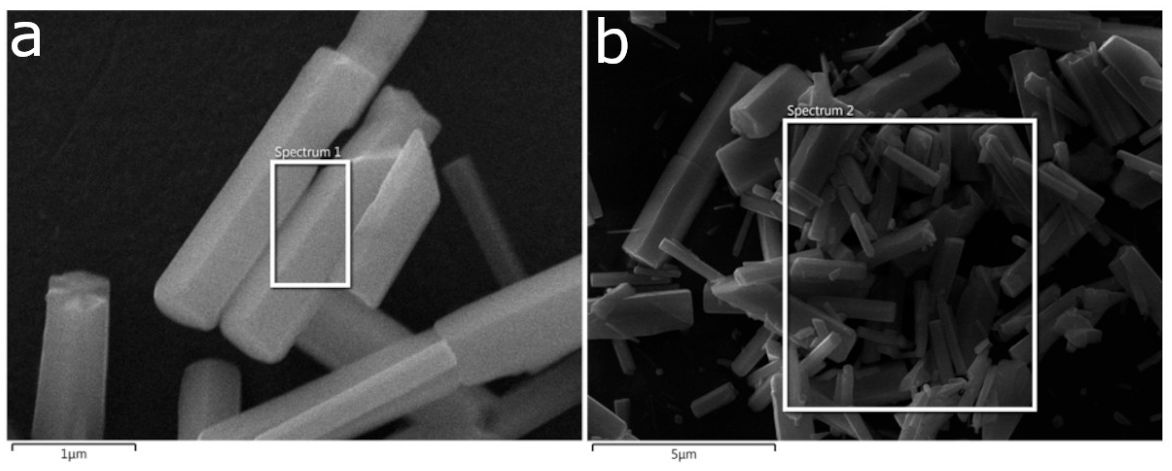
Morphology and chemical composition were obtained via Scanning Electron Microscopy (SEM) and Energy Dispersive Spectroscopy (EDS), using a JEOL JSM-7600F scanning electron microscope (Peabody, MA, USA). The considered area for EDS measurements of samples synthesized with system CBD-HVEF-A consists only of the ZnO rods; measurements were taken by using and accelerating a voltage of 15 kV, as shown in Figure 2. The chemical composition for each sample resulted from the average EDS measurements from rods of three different areas of the sample. In addition, the chemical compositions resulting from the three measurements where very similar, indicating homogeneity in the rods that conform the coating. Meanwhile, for samples synthesized by using CBD-HVEF-B, EDS measurements were taken over an area of 2 × 1.5 mm2 of the ZnO sample and chemical composition resulted from the average of three different zones for each sample. Hyperspectral color mapping for samples synthesized by CBD-HVE-B was performed in order to observe uniformity on the elemental chemical composition, and the result for M7-S is reported as it was representative of the samples. The crystalline structure of samples synthesized by CBD-HVEF-A was obtained by X-ray diffraction using a BRUKER D8 ADVANCE diffractometer (Madison, WI, USA) and Cu-Kα radiation (λ = 1.5406 Å) with a step of 0.0202 degrees. The grain size (D) was calculated by using the Scherrer formula
D = K λ B c o s θ
where K is the Scherrer constant with a value of 0.9 for non-spherical crystallites, λ is the wavelength of the X-rays coming from the transition in Cu = 1.5406 Å, B is the peak broadening at half maximum intensity (FWHM), and θ is the Bragg angle which is half the angle of the diffraction peak (2θ).
Figure 2. Two SEM micrographs for one of the samples synthesized by CBD-HVEF-A. (a) Zone 1 and (b) zone 2; the rectangle shown in each micrograph indicates the area considered for EDS analysis.
Coatings 15 01225 g002
Absorption spectra of coatings obtained by CBD-HVEF-A were obtained by using two devices: (1) a Variant Cary 5000 UV-VIS-NIR spectrometer (Agilent, Santa Clara, CA, USA) in transmittance operating mode and (2) a Shimadzu UV-Vis spectrophotometer (Kyoto, Japan) in reflectance operating mode with an integrating sphere (UV-2600i, Kyoto, Japan).
All ZnO coatings exhibited a particle-like morphology, and particle dimensions were analyzed to elucidate the influence of the electric field and its polarity inversion and air injection. Micrographs were taken from at least three different areas of each sample, and since the coatings were homogeneous across the substrate, a high degree of similarity between these micrographs was observed. Therefore, one of these was selected as representative of the coating’s surface morphology. The SEM images considered for ZnO coatings synthesized by CBD-HVEF-A and CBD-HVEF-B were those with a magnification of 2000× and 50,000×, respectively. Particle sizes were subsequently measured using Image J software version 1.54g, and these values were represented using a frequency distribution bar graph. The bin size was appropriately selected to subsequently calculate its size distribution curve using Origin 2018 software.

3. Results and Discussion

3.1. SEM

The analysis of SEM micrographs of the samples shows that the surface of all films is formed by rod-shaped particles of micro or nanometric dimensions, which is consistent with the results obtained by other authors [23], as well as notable differences in said dimensions, according to the deposition conditions listed in Table 1.
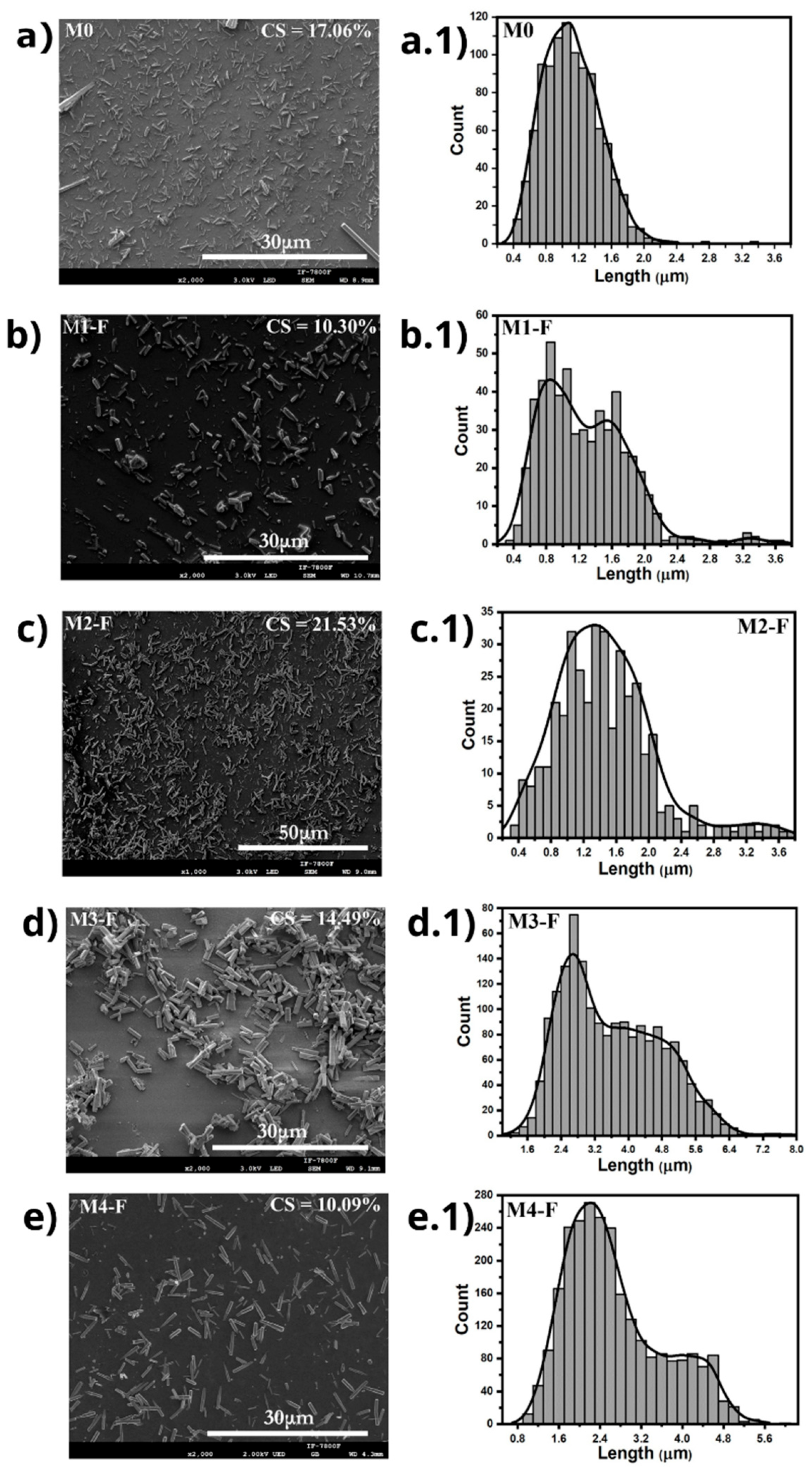
Figure 3 presents SEM micrographs of the samples synthesized by CBD.HVEF-A; these micrographs show that the ZnO coatings have rod-shaped microparticles in their composition. The sizes of the rods in the samples were measured and their corresponding size distribution functions are shown in Figure 3. In order to measure the percentual quantity of rod-shaped microparticles present on the ZnO coating (CS), a program designed in Mathematica Software version 11.3 [24] was employed, and the corresponding obtained values are presented in each micrograph.
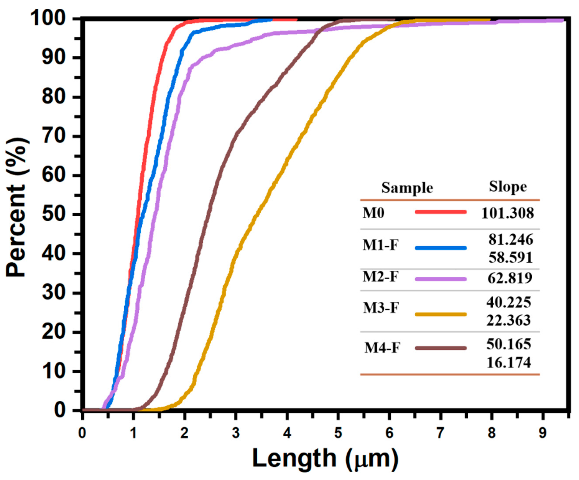
Table 2 presents the descriptive statistics that summarize the information from the size distribution functions for each sample synthesized by CBD-HVEF-A shown in Figure 3. The distribution function along with the cumulative curves for these samples (Figure 4) shows that the application of an electric field results in a dispersion and increase in the rod sizes, as the mean size went from 1.092 μm in sample M0, with no electric field applied, to 1.271 μm and 1.631 μm for samples M1-F (36 kV) and M2-F (24 kV), respectively, and interquartile range went from 0.486 μm for sample M0 to ≈0.76 μm in both M1-F and M2-F samples in which an electric field was applied, meaning that although dispersion in the rod size increased with the electric field, the value looks to be independent of the intensity of the electric field. When looking at SEM images for samples M3-F and M4-F, it is evident that the resulting particles maintain the same rod structure as other samples, although a quick glance at the average particle size confirms that in both cases, these rods are considerably larger when comparing them to M1-F, where no inversion of the electric field occurred, and being larger than M3-F modes in a ratio of 3.17:1 and 2.36:1, as well as 2.70:1 and 2.61:1 for M4-F. Furthermore, both samples M3-F and M4-F maintain the bimodal distribution function of sample M1-F, which is a good indicator of the consistency in the synthesis process that occurs when an electric field of 36 kV is applied, regardless of whether polarity inversion is applied or not. The interquartile range allows us to see that the dispersion in the rod size increases further with the polarity inversion in the electric field, increasing in M3-F, which has a higher inversion frequency (shorter period), which agrees with the fact that longer periods should behave as if no inversion occurs.
Figure 4 presents the cumulative curves of the length of the ZnO rods in samples synthesized by CBD-HVEF-A, where a higher slope indicates a lower dispersion of the rod lengths, the apparition of more than one “linear” segment is a consequence of multi-modal distribution functions, and the number of segments indicates the number of modes. This being said, the application of an electric field during the synthesis of ZnO results in higher dispersion rates and bi-modal functions. The slope values of each cumulative curve are inserted in the figure to show a quantitative measure of length dispersion. These curves make even more evident what was stated above: the application of an electric field results in an increase in particle length in all cases; to a greater degree, for samples with inversion of polarity, sample M3-F, synthesized under a 36 kV electric field with electrical polarity reversal every 2.5 min, is the one with the largest particles and the greatest dispersion in size.
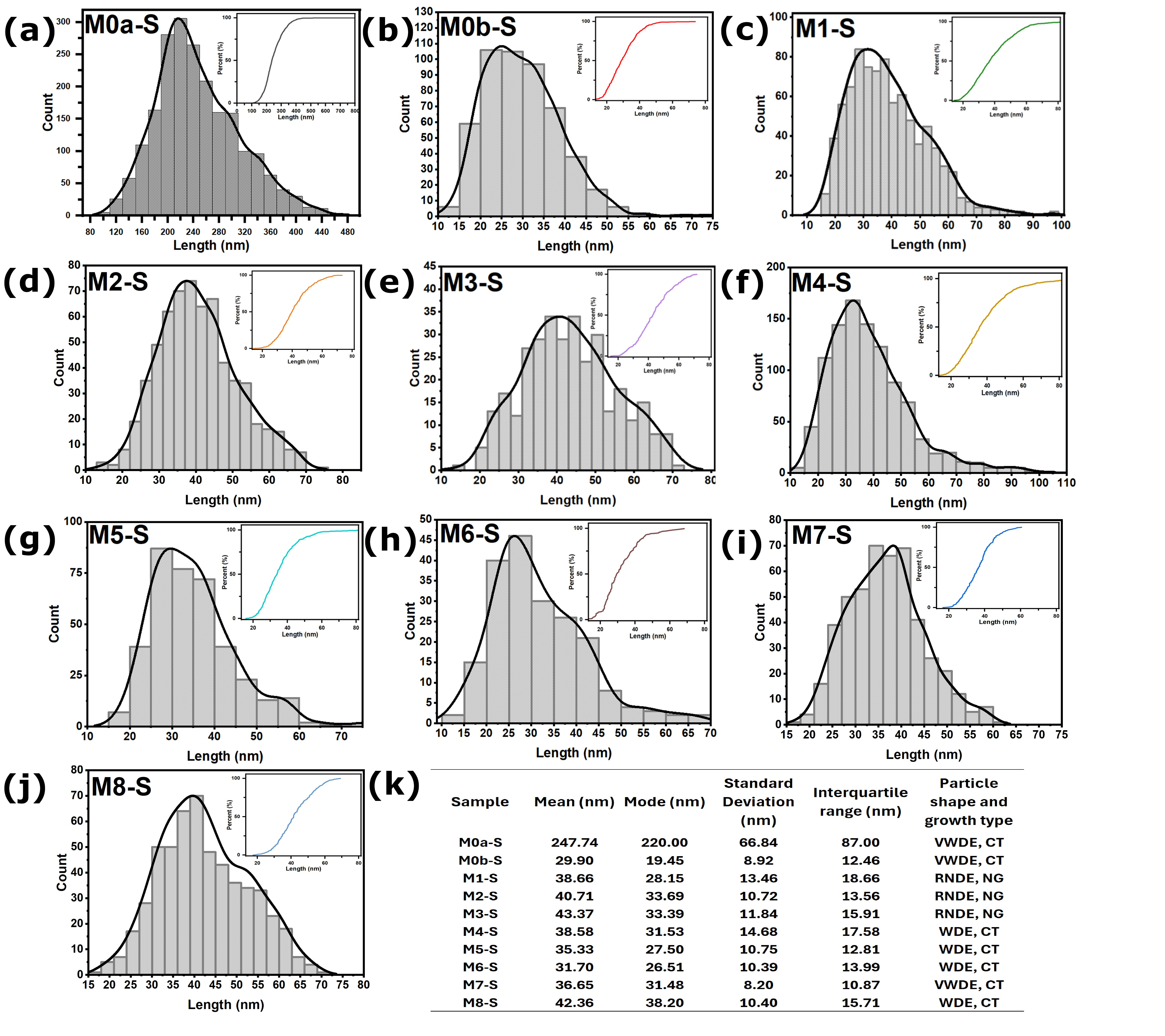
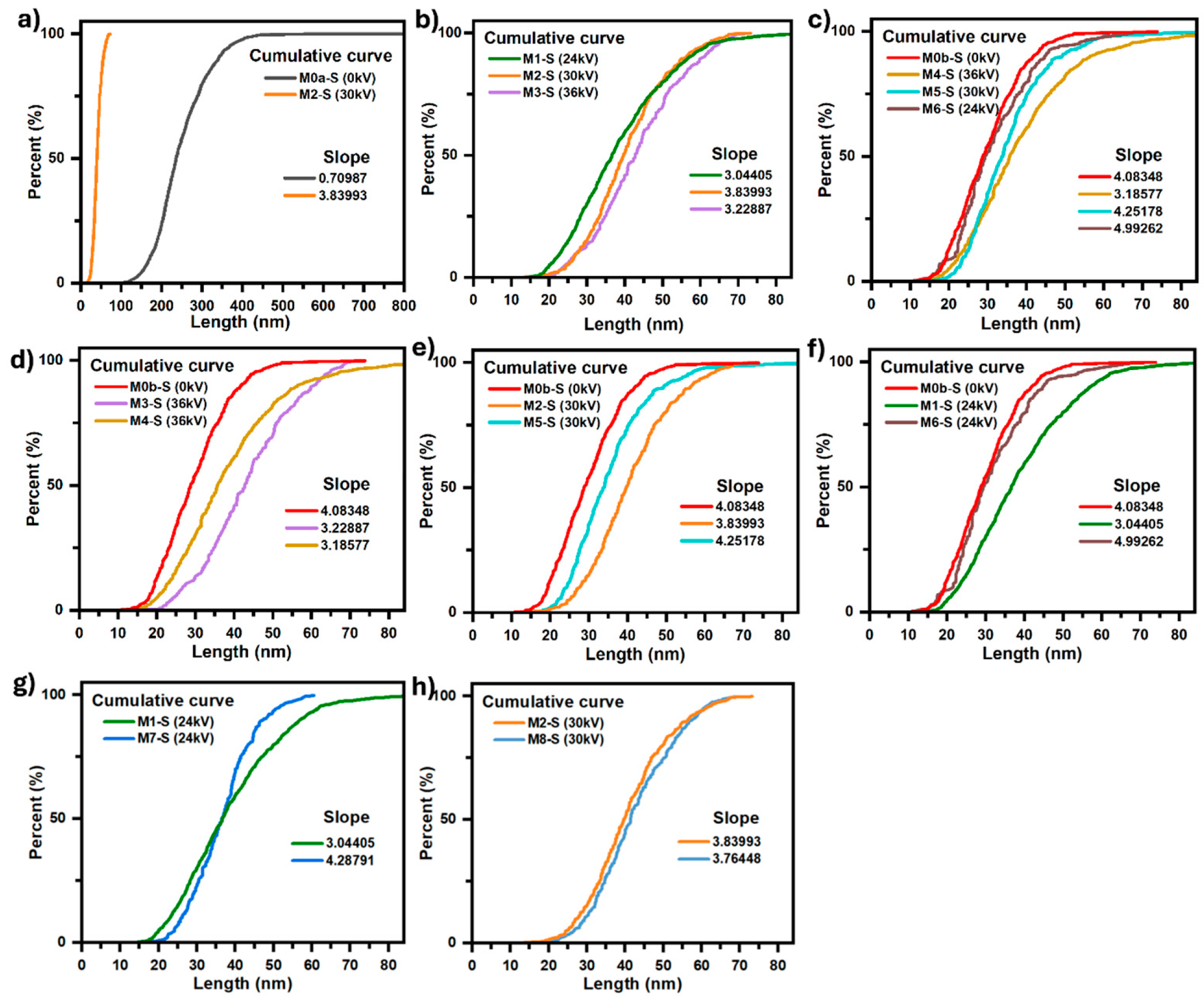
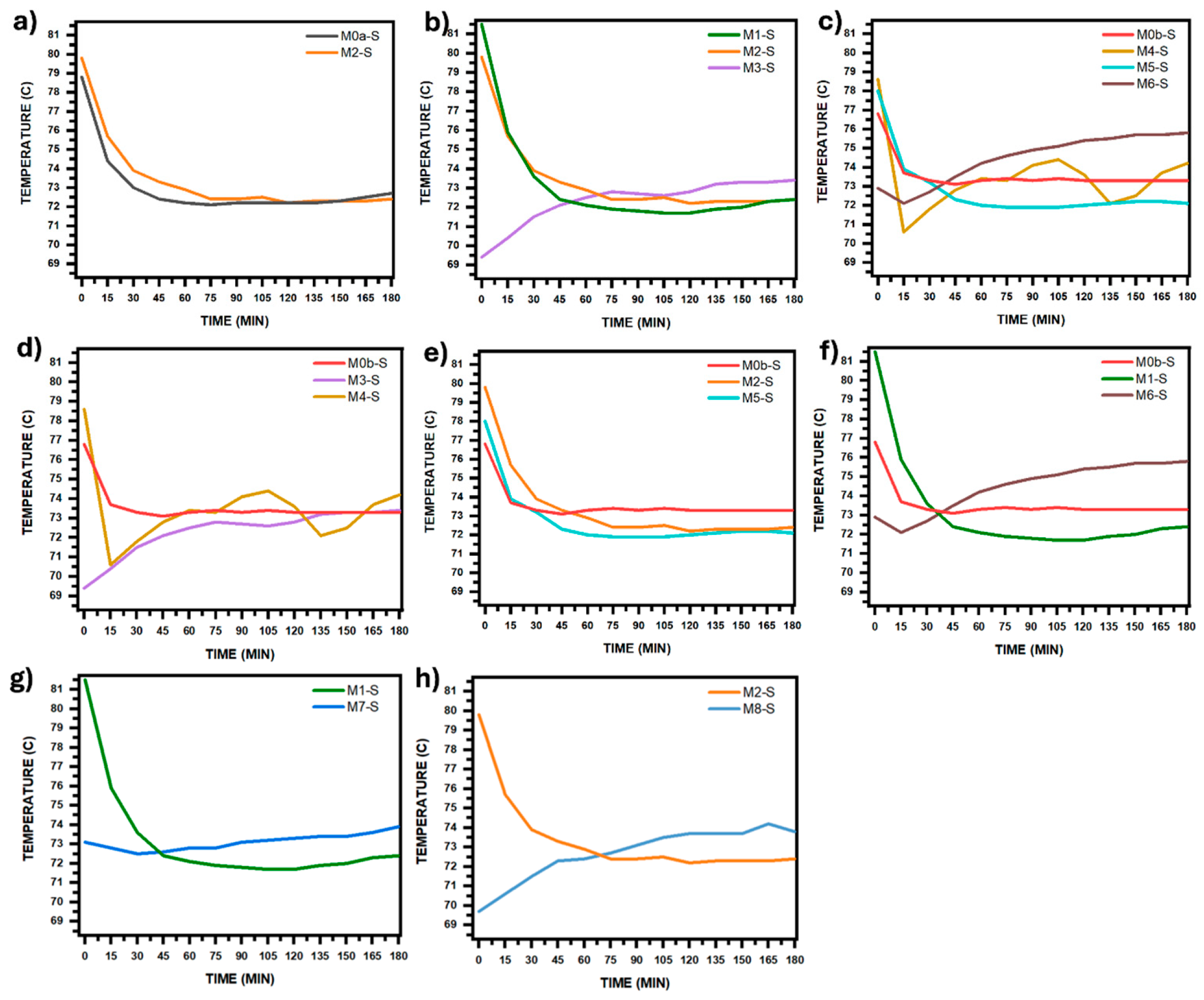
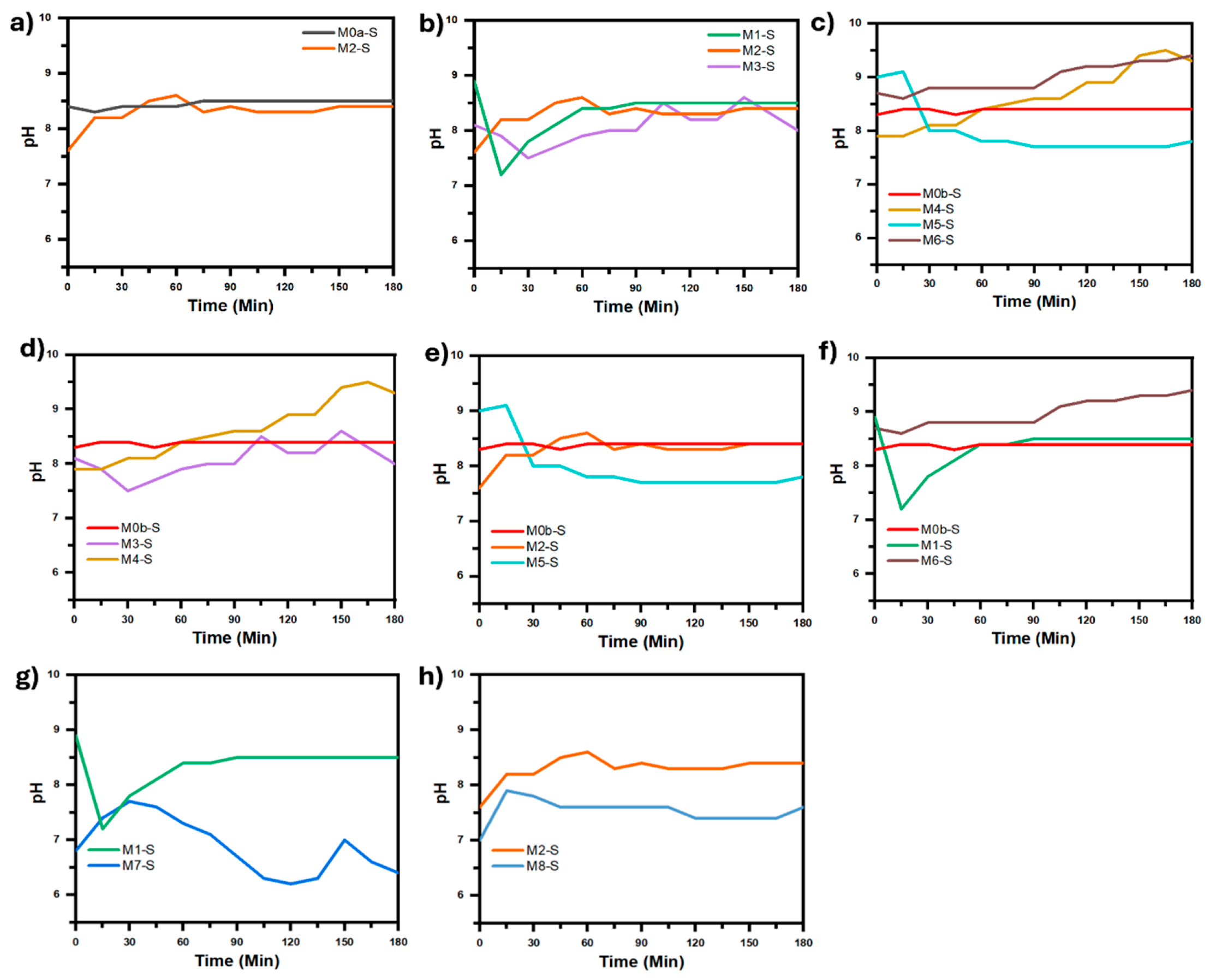
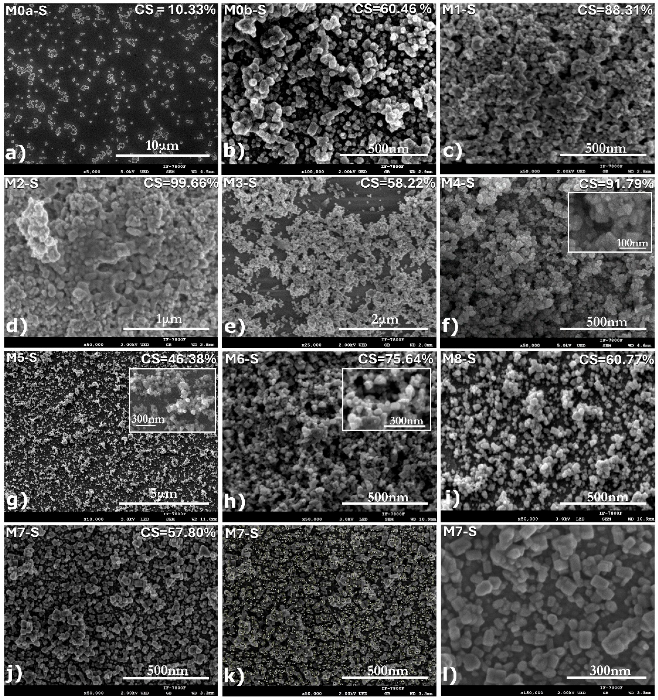
Figure 5 presents micrographs for samples obtained using the CBD-HVEF-B system, each labeled according to the corresponding sample listed in Table 1. These micrographs showed homogeneity in the ZnO deposit as well as the fact that all the coatings were composed of nanometric-sized particles, except for M0a-S, which is the sample deposited by a conventional CBD technique and was composed of submicrometric particles. Each micrograph has an insert with the percentage value of the substrate area coated by these submicrometric ZnO particles, obtained using software developed by our research team and employed in previous reports [24]. The characteristic shape of the particles and the descriptive statistics of their sizes are presented in the table inserted in Figure 6. The same figure also shows the particle size distribution functions for all the coatings, in correspondence with the micrographs in Figure 5. There, next to each of the size distribution functions, their corresponding cumulative size curves are presented. The comparative analysis between the coatings, in terms of the shape and size of the particles that compose them, was carried out based on whether or not an electric field was used during the synthesis and whether or not the solution was stirred by injecting filtered air into it, in addition to the variation in its pH, thus resulting in eight comparative analyses between the coatings. Figure 7 shows the different cumulative size curves of the coatings according to the comparative analysis in question. Likewise, Figure 8 and Figure 9 show the temperature and pH curves of the solution during synthesis process, corresponding to each comparative analysis in Figure 7, this is in order to assess whether or not there are significant differences between the temperature and pH curves that should be considered for the corresponding analysis.
Figure 5. SEM micrographs of the films obtained using CBD-HVEF-B (ai); each image is labeled to its corresponding sample in the upper right corner. The film synthesis parameters are shown in Table 1. The percentage of the substrate area covered by submicron ZnO particles is indicated in the upper right corner of each micrograph. Additional micrographs for sample M7-S ((jl), also labeled in the upper left corner) show how size analysis was performed using Image J software as well as the shape of the ZnO nanocrystals with hexagonal-prismatic morphology.
Coatings 15 01225 g005
Figure 6. Particle size histograms of the films obtained with CBD-HVEF-B ((aj), each histogram is labeled to its corresponding sample on the upper left corner). Its corresponding cumulative percentage curve is inserted in the upper right corner. The table (k) shows the descriptive statistics for the samples and the characteristic shape of their submicron ZnO particles—Very-Well-Defined Edges (VWDE), Well-Defined Edges (WDE) and Rounded, Not-Defined Edges (RNDE)—and the type of growth: nodular (NG) or columnar type (CT).
Coatings 15 01225 g006
Figure 7. Comparative analysis between the length and size dispersion of the particles that make up the samples, by comparing their corresponding cumulative curves. (a) Effect of electric field. (b) Effect of electric field intensity. (c) Effect of both: stirring with filtered air and electric field intensity. (df) Effect of stirring with filtered air. (g,h) Effect of pH change.
Coatings 15 01225 g007
Figure 8. Temperature curves of the precursor solution during the synthesis process. The curves were grouped according to each comparative analysis in Figure 7: (a) Effect of electric field. (b) Effect of electric field intensity. (c) Effect of both: stirring with filtered air and electric field intensity. (df) Effect of stirring with filtered air. (g,h) Effect of pH change.
Coatings 15 01225 g008
Figure 9. pH curves of the precursor solution during the synthesis process. The curves were grouped according to each comparative analysis in Figure 7: (a) Effect of electric field. (b) Effect of electric field intensity. (c) Effect of both: stirring with filtered air and electric field intensity. (df) Effect of stirring with filtered air. (g,h) Effect of pH change.
Coatings 15 01225 g009
The comparison between micrographs of samples M0a-S and M2-S, Figure 5a and Figure 5d, respectively, clearly shows the influence of the electric field during the CBD synthesis process. It can be observed that the conventional CBD coating M0a-S covers only 10.33% of the ITO substrate surface, while the coating whose synthesis was assisted by the electric field (M2-S) covers 99.66% of the surface, and the particles that make up the coating went from being nanocrystals with hexagonal-prismatic morphology of dimensions in the order of 247 nm with very-well-defined edges in M0a-S to particles with rounded edges and practically no defined corners; the average dimension for M2-S was 40.71 nm with a mode of 33.69 nm, thus reducing its size by six times (see table inserted in Figure 6). This reduction in particle size is even better appreciated by comparing the cumulative size curves for both coatings, see Figure 7a, as the electric field can enhance the nucleation rate; a higher number of nuclei implies smaller average particle size and consequently that particle size distribution shifted towards smaller diameters. A comparative analysis of the micrographs corresponding to the M0a-S and M0b-S coatings (Figure 5a and Figure 5b, respectively), both synthesized in the absence of an electric field, reveals that stirring the precursor solution with filtered air injection markedly decreases the particle size. This effect, analogous to that induced by an electric field, results in a greater size reduction (up to twelvefold), yielding an average of 29.90 nm and a mode of 19.45 nm (see table in Figure 6). The coatings maintain a hexagonal-prismatic morphology with well-defined edges and predominantly perpendicular orientation to the substrate, although ZnO coverage decreases to approximately 60.46%. In summary, applying an electric field or stirring the solution through the injection of filtered air led to a higher growth rate of ZnO and a reduction in the size of the particles that make up the coating, in addition to the fact that the electric field promoted the aggregation of the nanoparticles, which resulted in a much more compact coating.
Micrographs associated with coatings M1-S, M2-S, and M3-S (Figure 5c–e) were compared to study the effect of the electric field intensity on the coating morphology, this for electric fields produced by potential differences between electrodes of 24, 30, and 36 kV, respectively. It was observed that the morphology of the coatings was similar, independent of the field intensity, observing a nodular-type growth followed by a coalescence process between particles. The degree of aggregation of the particles, as well as the percentage of the covered substrate area, were greater for 30 kV, covering up to 99.66% of the substrate surface, while for 24 and 36 kV it was 88.31 and 58.22%, resulting in a coating with greater compactness for 30 kV. When comparing the cumulative particle size curves, Figure 7b, it is observed that the particle size grows slightly by 16.9% when the potential difference goes from 24 to 36 kV, as well as a variation in the dispersion of their sizes; the latter is noticeable by the relative change in the slope of the curves (see values in the same figure), with the dispersion being lower for 30 kV where the slope of the curve is greater, which is consistent with its interquartile range of 13.56 nm (see table in Figure 7), while for the coatings obtained at 24 and 36 kV, the interquartile range was 18.66 and 15.91 nm, respectively.
To study the effect that the intensity of the electric field in combination with the injection of filtered air has on the coating morphology, micrographs for M4-S, M5-S, and M6-S were compared for 36, 30, and 24 kV, respectively (see Figure 5). It is observed that the coating that now presents greater compactness is the one obtained at 36 kV and not at 30 kV, as it was when the solution was not stirred with filtered air, and that the substrate coverage reached up to 91.79% for 36 kV, while for 30 and 24 kV it was 46.36 and 75.64%, respectively. Figure 7c presents the cumulative size curves for the three coatings, as well as the curve for the one in which only air injection was applied (M0b-S); as can be seen, applying an electric field in addition to air injection has the effect of increasing the average particle size in such a way that when its intensity is increased, this effect is even greater, going from an average size of 26.5 nm for a field produced by 24 kV to 31.5 nm for that produced by 36 kV. The same also occurs with the size dispersion, as can be seen through the decrease in the slope of the curve as the field intensity increases (values are in the same figure), going from 4.99 to 3.19 for 24 and 36 kV, respectively.
To further highlight the effect that applying an electric field and air injection have together on the average particle size that constitute the coating and the dispersion of their sizes, Figure 7e presents the cumulative size curves for the M0b-S, M2-S, and M5-S coatings, the synthesis of which was assisted by air injection for M0b-S, an electric field produced by a voltage of 30 kV between electrodes for M2-S, and an electric field of 30 kV in addition to air injection for M5-S. These cumulative curves show how the effects of the electric field and the air injection on the size of the particles that make up the M5-S coating overlap, giving rise to a film made up of nanoparticles with an average size of 35.33 nm and a mode of 27.50 nm, which are intermediate values between the average sizes and modes values for when only air injection is applied, (M0b-S) 29.90 nm and 19.45 nm, and when only electric field is applied, (M2-S) 40.71 nm and 33.79 nm. Likewise, Figure 7d–f show how the effect of the electric field on the size of the particles is shielded by the effect that air injection has on them. It is observed that as the intensity of the electric field is reduced, the size of the particles becomes increasingly similar to that obtained by only injecting filtered air into the precursor solution. Now, regarding the morphology of the coating, it is observed that applying an electric field, in addition to air injection, does not affect the columnar-type growth that ZnO presents with only air injection; it is even also possible to observe ZnO nanocrystals with hexagonal faces parallel to the substrate surface in the M5-S coating (30 kV), for which the coverage of the substrate surface was lower, around 46.38%. In the M6-S (24 kV) and M4-S (36 kV) coatings, the amount of material deposited on the substrate is such that the growth of ZnO nanocrystals with hexagonal faces parallel to the substrate surface cannot be seen.
In order to determine the effect of the pH of the precursor solution on the coating morphology and particle sizes that comprise it, a comparison was made between micrographs of M1-S vs. M7-S and micrographs of M2-S vs. M8-S that were synthesized only under the influence of an electric field, and with the same synthesis conditions between them, except for the pH of the solution, which between the coatings M1-S and M7-S, synthesized at 24 kV, had a pH difference of up to 2.5 (Figure 7g), while between M2-S and M8-S, synthesized at 30 kV, the pH difference was never greater than 1 (Figure 7h). In both comparisons it is observed that when the pH decreases the coalescence between the particles that make up the coating decreases notably to such an extent that it is practically imperceptible, in addition to the fact that the average size of the particles that make up the coating practically does not change; however, the dispersion of the particle sizes decreases notably when the pH decreases to such an extent that the solution goes from alkaline to acidic, which can be seen in Figure 7g, with the significant increase in the slope of the cumulative size curve for M7-S with respect to M1-S.

3.2. EDS

Table 3 shows the elemental chemical composition obtained by EDS analysis of the most significant samples resulting from the use of both systems: CBD-HVEF-A and CBD-HVEF-B. When comparing the Zn contents of samples M1-F, M3-F, and M4-F, it is observed that the samples synthesized by periodically inverting the field have a higher Zn content (M3-F and M4-F), being greater to the shorter inverting time. This indicates that there is more Zn content in M3-F than in M1-F and, having performed the chemical analysis directly on the ZnO rods for both samples, the ZnO rods in M3-F, obtained by reversing the polarity of the electric field, could have better stoichiometry than those obtained in M1-F without reversing the polarity, and further studies such as X-ray Photoelectron Spectroscopy would allow for a better study of stoichiometry, but this is beyond the scope of this first report of the work.
As for the ZnO synthesized by CBD-HVEF-B, it can be observed from Table 3 that the chemical elemental contents for samples M0a-S and M0b-S are very similar, so the injection of air into the precursor solution does not affect the chemical composition of the synthesized zinc oxide; likewise, the contents of M1-S, M2-S, and M4-S are similar to each other, indicating that the variation in the electric field intensity alone or with air injection does not promote significant changes in the chemical composition of synthesized zinc oxide; however, one may think that the contents of M6-S indicate otherwise, but these are still similar to the contents of M1-S, M2-S, and M4-S if one considers that the penetration of the electron beam into the substrate during the analysis was lower, as reflected in the lower contents of the chemical elements associated with the substrate. However, as stated above, it is necessary to delve into the study of the elemental chemical composition of the synthesized material without involving the substrate, but that study is beyond the scope of this first report.
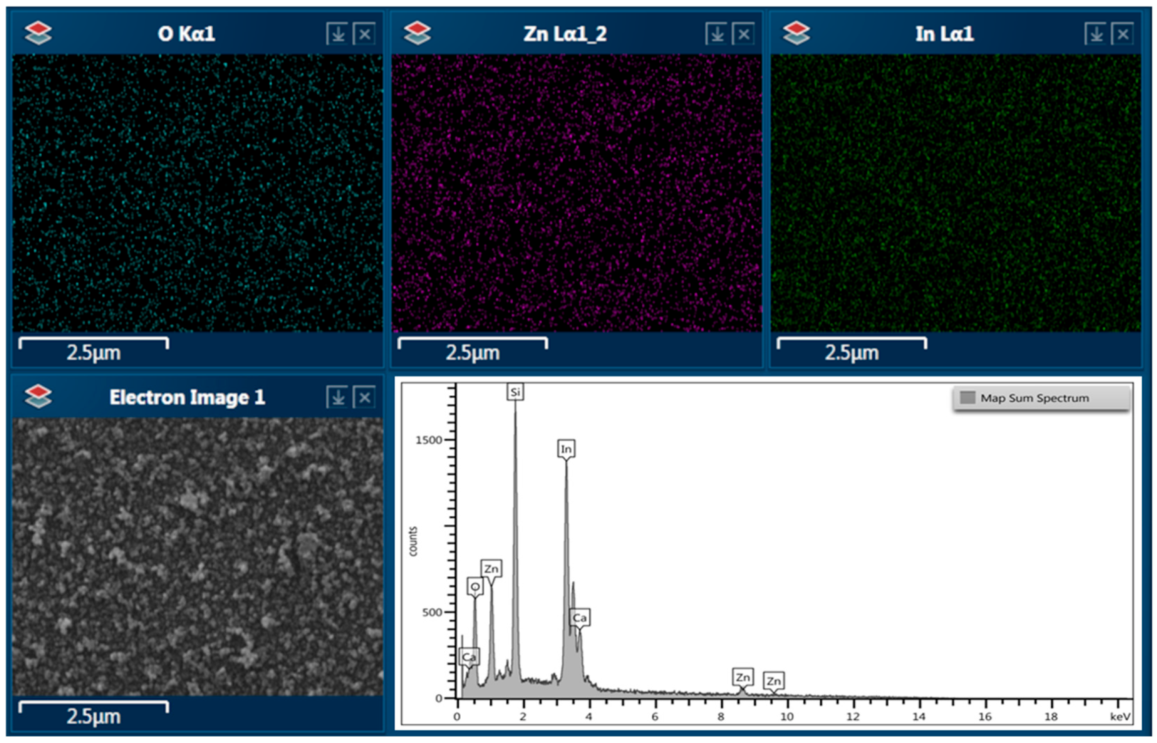
Figure 10 shows the hyperspectral color mapping for sample M7-S, which was representative of the samples synthesized by CBD-HVE-B. All mappings show uniformity in the chemical composition for the samples.

3.3. X-Ray Diffraction

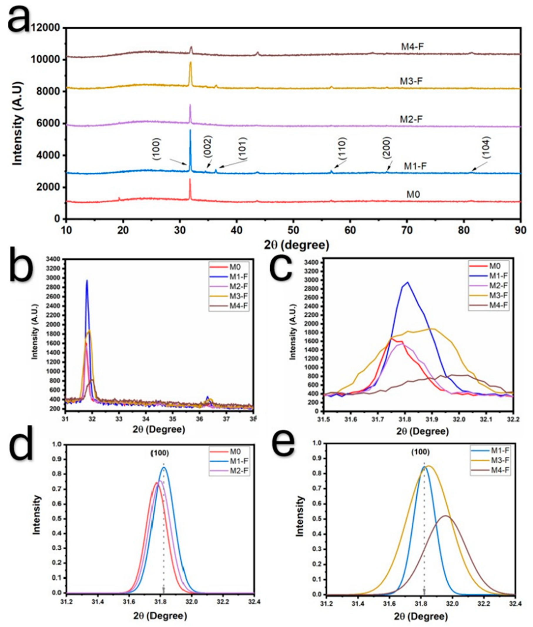
Figure 11a shows the XRD patterns for samples synthesized by using the CBD-HVEF-A system. The diffraction patterns were indexed to crystallographic card JCPDS No. 076-0704, corresponding to the hexagonal wurtzite phase of ZnO. In all samples the (100) peak had the highest intensity, which suggests a preferential growth in the [100] direction. Figure 11b and Figure 11c show close-ups of two different regions of the XRD patterns corresponding to peaks (100), (101), and (002) and peak (100), respectively. At first glance, it is evident that there is a significant widening in the peaks as well as a shifting of their maxima towards greater angles; this suggest a non-uniform compression of the crystalline cell.
For closer examination on shifting and broadening of the (100) peak, Figure 11d,e present its gaussian fit, which was also normalized by each maximum, and its corresponding baseline was subtracted. It can be observed that (100) peaks for samples M1-F and M2-F are shifted to greater angles when comparing them to sample M0, which had no electric field applied, as can be seen in Figure 11d. This shift signals a reduction in the interplanar distance of (100) planes for these samples. Therefore, one could state that the application of an electric field during synthesis can result in a reduction in interplanar distance, which is greater when a higher voltage between plates is used, as is the case for M1-F. In addition, when maintaining a constant voltage of 36 kV but periodically inverting the direction of the electric field, Figure 11e shows that for peak (100) there is a shift towards larger angles as well as a broadening, this in comparison with peak (100) of sample M1-F, which has the same synthesis conditions but no inversion of electric field. For higher inversion frequency, in sample M3-F, there is a major broadening of the diffraction peak, which implies a smaller grain size, along with a reduction in the interplanar distance between (100) planes, as indicated by the shift in its diffraction angle, this also occurs for sample M4-F, although in this case, grain size reduction is still significant but less than that of M3-F, with an even smaller interplanar distance. Table 4 shows the calculated values for interplanar distance and grain size, considering peak (100), where it is even more evident how polarity inversion of the electric field promotes a decrease in interplanar distance along with a big reduction in grain size to around half of the value obtained by no inversion.

3.4. Absorbance

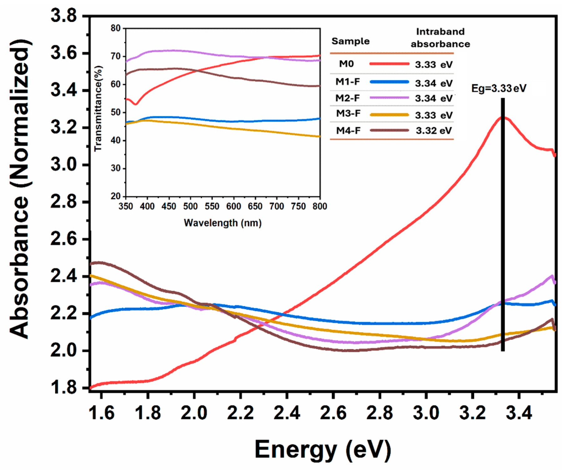
Figure 12 presents the absorbance spectra for samples synthesized by CBD-HVEF-A obtained by using a Cary 5000 UV-Vis-spectrometer (Agilent, Santa Clara, CA, USA); the values of their respective intraband absorption energies are summarized in the table inserted in the same figure. The insert of Figure 12 shows the corresponding transmittance spectra. The intraband absorption energy values were obtained through the first and second derivatives of the absorbance curves. There is an evident blue-shift of ~5 nm in all samples as an effect of the applied electric field during synthesis, with the exception of M4-F. This blue shift of ~5 nm indicates a constant increase in the band gap of the material as a result of the electric field applied independently of its intensity or if its polarity was inverted. This is inconsistent with the diffraction angle shift to larger values observed in the XRD patterns, since a lower interplanar distance translates into a higher crystalline field, and shorter Zn–O bond in-plane distances strengthen the electrostatic crystal field interaction, enhancing Zn 3d–O 2p hybridization and causing a greater upward shift in the valence band maximum (VBM). In contrast, the Zn 4s orbitals forming the conduction band minimum (CBM) are less sensitive to bond shortening than the O 2p/Zn 3d states. As a result, the valence band rises more significantly than the conduction band shifts, leading to a reduction in the bandgap. More studies are needed to resolve this discrepancy, which should consider the non-homogeneous (100) interplanar reduction observed in XRD patterns.
Regarding the absorption of ZnO in the visible spectrum, commonly associated with the presence of intrinsic defects in its crystalline structure, it is observed that while sample M0 deposited by conventional CBD presents an absorption that begins at 550 nm and becomes more intense as it approaches the blue, none of the samples grown by CBD HVEF-A present this absorption (see Figure 12). This absorption is commonly associated with oxygen defects and/or interstitial zinc [25], so in principle it can be observed that deposition by CBD-HVEF-A inhibits the formation of these types of intrinsic defects. When comparing the transmittance spectra of the samples grown by CBD HVEF-A, it is clear that sample M1F is the one that in principle presents the fewest intrinsic crystalline defects, since it only presents a slight absorption centered at 2.05 eV, which is commonly associated with the presence of hydroxyl (OH) groups as an emission center, particularly present in synthesis methods involving aqueous solutions [25], while M2-F, M3-F, and M4-F presented, in addition to this absorption, an absorption centered at 1.59 eV, commonly associated with hydrogen impurities [26,27,28].
Figure 13 presents the absorbance spectra for samples synthesized by CBD-HVEF-A obtained using a Shimadzu UV-Vis spectrophotometer as well as their corresponding Tauc plots. At first glance, in the Tauc plots it can be seen that all samples appear to have the same energy gap (Eg) value of 3.10 eV; however, once you zoom in on the region between 3.00 and 3.30 eV, inserted in Figure 13b, you can see that there is a slight but noticeable difference between the Eg values of the samples as a result of the electric field applied, independent of its intensity or if its polarity was inverted. These Eg values are listed in the table inserted in Figure 13b.
Regarding the absorption of ZnO in the visible spectrum, it is observed that samples with absorption at 449 nm would correspond to an intraband level situated 2.76 eV above the valence band, and has been widely associated by several authors with zinc interstitial (Zni) defects and their extended energy levels (ex-Zni) that act as shallow donors [25,29,30]. Additionally, the absorption situated at 556 nm has also been previously reported by Lizarraga, et al., who determined it could be linked to Zni. As for the peak present at 704 nm (about 1.76 eV) it is not commonly documented in the literature as being linked to a particular intrinsic defect, although a few authors do report that luminescence in this particular energy field could be linked to oxygen interstitials (Oi) [31], but further studies would need to be carried out to associate this absorption to a particular defect, which constitutes interesting future work. The fact that the relative intensities of the 449, 556, and 704 nm bands in the samples remain practically constant means that the relative concentrations of intrinsic Zni and Oi defects in all samples are practically the same. This result is atypical since the relative concentration of intrinsic defects is very sensitive to variations in the synthesis parameters. Other studies such as FTIR and Raman spectroscopy are needed to resolve the relative concentrations of intrinsic defects to elucidate this atypical result.

3.5. General Discussion

The application of a high-intensity electric field during the CBD of ZnO thin films introduces significant electrostatic and electrochemical effects that strongly influence nucleation kinetics, ion transport, and film morphology. In conventional CBD, film growth proceeds through ion-by-ion and hydroxide cluster mechanisms, where Zn2+ and OH species either react directly on the substrate surface or form Zn(OH)2 colloids that subsequently dehydrate into ZnO. In the absence of an electric field, ion mobility is primarily governed by diffusion and convection, allowing for homogeneous nucleation in the bulk solution. The application of an external electric field, however, promotes directional ionic migration, enhancing heterogeneous nucleation and improving film compactness and uniformity.
Additionally, the electric field induces water electrolysis, generating OH ions and shifting the precursor solution toward alkaline conditions that favor heterogeneous over homogeneous nucleation. This effect was confirmed by the reduced compactness observed in films synthesized from acidic precursors compared with those obtained under alkaline conditions. Increasing field intensity further enhanced film compactness, reaching an optimum at 30 kV, consistent with the preferential promotion of heterogeneous nucleation.
At the substrate–solution interface, the electric field compresses the electric double layer, thereby reducing the nucleation energy barrier and facilitating uniform film formation. The combined effects of field-induced ion migration and electrochemical modification of the bath yield ZnO films with improved coalescence, crystallinity, and surface coverage. In particular, the CBD-HVEF-B configuration at 30 kV produced highly compact ZnO layers with minimal particle size dispersion, confirming the beneficial role of electric field-assisted CBD in tailoring ZnO film microstructure and growth behavior.
4. Conclusions

ZnO coatings of the group A system were confirmed to exhibit the hexagonal wurtzite crystalline structure. Structural, morphological, and optical analyses demonstrated that applying a high-voltage electric field during synthesis markedly influences the crystallographic and morphological features of the films. The electric field promoted a reduction in the interplanar distance of the (100) planes and induced peak broadening, particularly under periodic polarity inversion at 36 kV, which also reduced grain size. SEM analysis revealed rod-shaped ZnO particles whose dimensions and distribution depend strongly on the electric field conditions. The application of a constant field increased both particle length and dispersion, while polarity inversion amplified these effects, leading to broader and often bimodal or multimodal particle size distributions. These results indicate that periodic polarity inversion modulates nucleation and growth kinetics, significantly altering the structural and morphological evolution of ZnO. Overall, electric field-assisted CBD enables precise control of ZnO film properties and provides a promising route for tailoring materials for optoelectronic applications through controlled field modulation.
ZnO coatings of group B showed a strong dependence between morphology and substrate coverage on the applied synthesis parameters. The application of an electric field substantially increased substrate coverage (up to 99.66%) and reduced average particle size (up to sixfold) compared to conventional CBD. Air injection stirring of the precursor solution also produced smaller particles (up to twelvefold reduction), although with lower coverage, while promoting the formation of well-defined columnar structures oriented perpendicularly to the substrate. When combined, electric field and air injection exhibited a cumulative effect, yielding intermediate particle sizes and mixed morphologies that varied with field strength. The electric field intensity was found to be critical: 30 kV produced more compact and uniform coatings, whereas higher or lower intensities (24 and 36 kV) resulted in reduced coverage and greater dispersion. Additionally, lowering the precursor pH from alkaline to acidic conditions suppressed particle coalescence and decreased size dispersion, enhancing coating uniformity. These findings demonstrate that ZnO morphology, particle size, and uniformity can be effectively tuned by adjusting electric field intensity, air injection, and solution pH, providing a versatile platform for optimizing coating properties for diverse technological applications.

Author Contributions

Conceptualization, F.R.-B. and J.N.A.-R.; Methodology, J.B.C.-R., F.R.-B., J.N.A.-R., M.A.S.-A., R.M.-M., E.C.-G., E.L.-M., F.J.S.-R., C.A.-A., A.C.-R., S.J.C., J.J.M.-D. and M.G.-H.; Validation, F.R.-B. and J.N.A.-R.; Formal analysis, F.R.-B., J.N.A.-R. and E.L.-M.; Investigation, J.B.C.-R., F.R.-B., J.N.A.-R., M.A.S.-A., R.M.-M., E.C.-G., E.L.-M., F.J.S.-R., C.A.-A., A.C.-R., S.J.C., J.J.M.-D. and M.G.-H.; Resources, F.R.-B., J.N.A.-R., M.A.S.-A. and E.C.-G.; Writing—original draft, F.R.-B., J.N.A.-R., R.M.-M., E.L.-M. and M.G.-H.; Writing—review & editing, F.R.-B., J.N.A.-R. and E.L.-M.; Visualization, J.B.C.-R., F.R.-B., J.N.A.-R., M.A.S.-A., R.M.-M., E.C.-G., E.L.-M., F.J.S.-R., C.A.-A., A.C.-R., S.J.C., J.J.M.-D. and M.G.-H.; Supervision, F.R.-B. and J.N.A.-R.; Project administration, F.R.-B. and J.N.A.-R.; Funding acquisition, F.R.-B. and J.N.A.-R. All authors have read and agreed to the published version of the manuscript.

Funding

This research received publication funding by Coordinación General Para el Fomento a La Investigación Científica e Innovación del Estado de Sinaloa (CONFíE).

Institutional Review Board Statement

Not applicable.

Informed Consent Statement

Not applicable.

Data Availability Statement

The original contributions presented in this study are included in the article. Further inquiries can be directed to the corresponding authors.

Conflicts of Interest

The authors declare no conflict of interest.

References

  1. Wilson, N. Advancements in Material Synthesis Techniques and their Implications. Mater. Sci. Eng. 2024, 13, 694. [Google Scholar] [CrossRef]
  2. Schmidt, R.; Gonjal, J.P.; Morán, E. Microwave-Assisted Hydrothermal Synthesis of Nanoparticles. In CRC Concise Encyclopedia of Nanotechnology; T. & F. Group, Ed.; CRC Press: Boca Ratón, FL, USA, 2016; pp. 561–572. [Google Scholar]
  3. Tang, B.; Lu, Y.; Zhou, J.; Chouhan, T.; Wang, H.; Golani, P.; Xu, M.; Xu, Q.; Guan, C.; Liu, Z. Machine learning-guided synthesis of advanced inorganic materials. Mater. Today 2020, 41, 72–80. [Google Scholar] [CrossRef]
  4. Tayyab, M.; Zizhe, L.; Rauf, S.; Xu, Z.; Sagar, R.U.R.; Faiz, F.; Tayyab, Z.; Rehman, R.U.; Imran, M.; Waheed, A.; et al. Advanced fabrication techniques for polymer–metal nanocomposite films: State-of-the-art innovations in energy and electronic applications. Chem. Sci. 2025, 16, 3362–3407. [Google Scholar] [CrossRef] [PubMed]
  5. Schneller, H.; Waser, R.; Kosec, M.; Payne, D. Chemical Solution Deposition of Functional Oxide Thin Films; Springer: Berlin/Heidelberg, Germany, 2013. [Google Scholar]
  6. Strano, V.; Greco, M.G.; Ciliberto, E.; Mirabella, S. ZnO Microflowers Grown by Chemical Bath Deposition: A Low-Cost Approach for Massive Production of Functional Nanostructures. Chemosensors 2019, 7, 62. [Google Scholar] [CrossRef]
  7. Hodes, G. Semiconductor and ceramic nanoparticle films deposited by chemical bath deposition. Phys. Chem. Chem. Phys. 2007, 9, 2181–2196. [Google Scholar] [CrossRef] [PubMed]
  8. Sagadevan, S.; Das, I. Chemical bath deposition (CBD) of zinc selenide (ZnSe) thin films and characterisation. Aust. J. Mech. Eng. 2017, 15, 222–227. [Google Scholar] [CrossRef]
  9. Oliva, A.I.; González-Chan, I.J.; Várguez, P.E.; Trejo-Ramos, A.I.; Oliva-Avilés, A.I. The chemical process for materials deposition in aqueous solution: A review. Surf. Eng. 2022, 38, 907–929. [Google Scholar] [CrossRef]
  10. Guire, M.; Bauermann, L.; Parikh, H.; Bill, J. Chemical Bath Deposition. In Chemical Solution Deposition of Functional Oxide Thin Films; Springer: Springfield, IL, USA, 2013; pp. 319–339. [Google Scholar]
  11. Wang, X.; Hu, W. Polydopamine thin film-assisted patterned chemical bath deposition of ZnO nanorods on arbitrary substrates. CrystEngComm 2017, 19, 6182–6188. [Google Scholar] [CrossRef]
  12. Arsad, A.Z.; Zuhdi, A.W.M.; Abdullah, S.F.; Chau, C.F.; Ghazali, A.; Ahmad, I.; Abdullah, W.S.W. Effect of Chemical Bath Deposition Variables on the Properties of Zinc Sulfide Thin Films: A Review. Molecules 2023, 28, 2780. [Google Scholar] [CrossRef]
  13. Di Mari, G.M.; La Matta, V.; Strano, V.; Reitano, R.; Cerruti, P.; Filippone, G.; Mirabella, S.; Bruno, E. Optimized Chemical Bath Deposition for Low Cost, Scalable, and Environmentally Sustainable Synthesis of Star-Like ZnO Nanostructures. ACS Omega 2024, 9, 38591–38598. [Google Scholar] [CrossRef]
  14. Zhao, Y.; Li, K.; Hu, Y.; Hou, X.; Lin, F.; Tang, J.; Tang, X.; Xing, X.; Zhao, X.; Zhu, H.; et al. The effect of the solution flow and electrical field on the homogeneity of Large-Scale electrodeposited ZNO nanorods. Materials 2024, 17, 1241. [Google Scholar] [CrossRef]
  15. Alba-Cabañas, J.; Rodríguez-Martínez, Y.; Vaillant-Roca, L. Effects on the ZnO nanorods array of a seeding process made under a static electric field. Mater. Today Commun. 2024, 39, 108917. [Google Scholar] [CrossRef]
  16. Lakhdari, M.; Habelhames, F.; Nessark, B.; Girtan, M.; Derbal-Habak, H.; Bonnassieux, Y.; Tondelier, D.; Nunzi, J.M. Effects of pulsed electrodeposition parameters on the properties of zinc oxide thin films to improve the photoelectrochemical and photoelectrodegradation efficiency. Eur. Phys. J. Appl. Phys. 2018, 84, 30102. [Google Scholar] [CrossRef]
  17. de la Mata, M.; Zamani, R.R.; Martí-Sánchez, S.; Eickhoff, M.; Xiong, Q.; i Morral, A.F.; Caroff, P.; Arbiol, J. The role of polarity in nonplanar semiconductor nanostructures. Nano Lett. 2019, 19, 3396–3408. [Google Scholar] [CrossRef] [PubMed]
  18. Koch, S.; Späth, S.; Shmeliov, A.; Nicolosi, V.; Mandel, K. Air bubble promoted large scale synthesis of luminescent ZnO nanoparticles. J. Mater. Chem. C 2015, 3, 12430–12435. [Google Scholar] [CrossRef]
  19. Abdulrahman, A.F.; Ahmed, S.M.; Ahmed, N.M.; Almessiere, M.A. Enhancement of ZNO nanorods properties using modified chemical bath deposition method: Effect of precursor concentration. Crystals 2020, 10, 386. [Google Scholar] [CrossRef]
  20. Shirvani, M.; Naji, L. Interface engineering of electrochemically deposited ZnO nanorods as electron transport layer in polymer solar cells using organic dyes. Mater. Chem. Phys. 2020, 259, 124064. [Google Scholar] [CrossRef]
  21. Guo, Q.; Dai, Y.; Qi, Y. Modulation of optical properties and defects of ZnO films with preferred orientations by annealing in different atmospheres. J. Chem. Phys. 2024, 161, 084701. [Google Scholar] [CrossRef]
  22. Toma, F.T.Z.; Rahman, S.; Maria, K.H. A review of recent advances in ZnO nanostructured thin films by various deposition techniques. Discov. Mater. 2025, 5, 1–31. [Google Scholar] [CrossRef]
  23. Alqaisi, M.M.; Ghazai, A.J. Optical Properties of Sn Doped ZnO Thin Film Prepared Using Sol-Gel Method for Optical Limiting Application. Al-Nahrain J. Sci. 2025, 24, 38–42. [Google Scholar] [CrossRef]
  24. Esmerio, C.L.; Rojas, C.R.; Rocha, J.A.; Medina, E.L.; Brito, F.R.; García, E.C.; Martinez, R.M.; Frutis, M.A.; Hipólito, M.G. Study of The Electrical, Optical and Morphological Properties in Submicron and Microstructured ZnO Thin Films Obtained by Spin Coating and Chemical Bath Deposition. Sci. Technol. Indones. 2022, 7, 291–302. [Google Scholar] [CrossRef]
  25. Lizárraga-Medina, E.; Ramos-Brito, F.; Aguilar-Frutis, M.; Angulo-Rocha, J.; Martinez-Martinez, R.; Sánchez-Alejó, M.A.; Alejo-Armenta, C.; Borja-Urby, R.; García-Hipólito, M. Pure ZnO with cool white, warm white, orange and turquoise color emissions: A purely experimental approach. Appl. Phys. A 2025, 131, 1–22. [Google Scholar] [CrossRef]
  26. Janotti, A.; Van de Walle, C.G. Native point defects in ZnO. Phys. Rev. B 2007, 76, 165202. [Google Scholar] [CrossRef]
  27. McCluskey, M.D.; Jokela, S.J. Defects in ZnO. J. Appl. Phys. 2009, 106, 071101. [Google Scholar] [CrossRef]
  28. Lavrov, E.V.; Weber, J.; Börrnert, F.; Van de Walle, C.G.; Helbig, R. Hydrogen-related defects in ZnO studied by infrared absorption spectroscopy. Phys. Rev. B 2002, 66, 165205. [Google Scholar] [CrossRef]
  29. Oba, F.; Choi, M.; Togo, A.; Tanaka, I. Point defects in ZnO: An approach from first principles. Sci. Technol. Adv. Mater. 2011, 12, 034302. [Google Scholar] [CrossRef] [PubMed]
  30. Zeng, H.; Duan, Y.; Yang, X.; Li, S.; Xu, X.; Cai, W. Blue Luminescence of ZnO Nanoparticles Based on Non-Equilibrium Processes: Defect Origins and Emission Controls. Adv. Funct. Mater. 2010, 20, 561–572. [Google Scholar]
  31. Ong, H.; Du, G. The evolution of defect emissions in oxygen-deficient and -surplus ZnO thin films: The implication of different growth modes. J. Cryst. Growth 2004, 265, 471–475. [Google Scholar] [CrossRef]
Figure 1. Diagrams of arrangements CBD-HVEF-A (a.1) and CBD-HVEF-B (b.1) for electric field-assisted bath deposition. Electric field is induced by (a) a voltage between two parallel plates placed on opposite outer walls of the glass container and (b) a voltage between the conductive substrate (ITO-coated glass) immersed in the precursor solution and a metallic plate placed on the outer wall of the glass container. (a.2), (a.3), and (a.4) are pictures of CBD-HVEF-A as set up in the lab, and (b.2), (b.3), and (b.4) are respective pictures of CBD-HVEF-B.
Coatings 15 01225 g001
Figure 3. Micrographs of the coatings obtained using CBD-HVEF-A (ae), as well as their corresponding size distribution functions (a.1e.1) for the ZnO rods in each of the samples. The percentage value of its area covered by ZnO is inserted in the upper right corner of each micrograph. Synthesis parameters are shown in Table 1.
Coatings 15 01225 g003
Figure 4. Cumulative curves of the length of the ZnO rods for synthesized samples using the CBD-HVEF-A system. The inset table shows the slope values for each sample.
Coatings 15 01225 g004
Figure 10. Hyperspectral color mapping for sample M7-S with its associated EDS spectrum.
Coatings 15 01225 g010
Figure 11. XDR patterns of all samples of the CBD-HVEF-A system. Indexed patterns (a). Enlargement of the XRD patterns considering the three main XRD peaks, (100), (002), and (101) (b). Enlargement of the (100) peak (c). Gaussian fit of the normalized (100) peak (d,e).
Coatings 15 01225 g011
Figure 12. Absorbance spectra for samples synthesized using the CBD-HVEF-A system. The inserted image and table correspond to their transmittance spectra and intraband absorption values, respectively.
Coatings 15 01225 g012
Figure 13. Absorbance spectra (a) and Tauc plots (b) for synthesized samples using the CBD-HVEF-A system. The image inserted in (b) is a magnification of the Tauc graphs showing the differences between the Eg values; these values are shown in the attached table.
Coatings 15 01225 g013
Table 2. Descriptive statistics of the distribution functions for each sample synthesized by CBD-HVEF-A shown in Figure 3.
SampleMean
(µm)
Mode
(µm)
Standard Deviation
(µm)
Interquartile Range
(µm)
M01.091.050.3610.486
M1-F1.270.850.5360.766
1.65
M2-F1.631.371.130.765
M3-F3.612.701.151.84
3.90
M4-F2.682.300.9421.28
 4.30
Table 3. Elemental composition of representative samples obtained using the CBD-HVEF-A and CBD-HVEF-B systems, determined by EDS. The symbol “*” indicates that the element was detected but not quantified.
Element Elemental Chemical Composition in Atomic Percent
M1-FM3-FM4-FM0a-SM0b-SM1-SM2-SM4-SM6-S
C********2.02
O58.5950.3055.7754.7353.4552.5750.9251.2951.07
Al   ****1.030.72
Si16.986.6910.759.4910.4014.5017.6316.906.54
Ca1.181.030.851.131.492.332.672.430.87
Zn23.2441.9832.6325.8625.2416.9915.3612.3829.35
In   8.799.4113.6113.4214.638.81
Sn   ****1.330.62
Table 4. Interplanar distance and grain size values for all samples, considering peak (100).
Samples2θ DegreeFWHMInterplanar Distance (Å)Grain Size (nm)
M031.780.00262.8254.84
M1-F31.820.00282.8151.47
M2-F31.800.00252.8152.05
M3-F31.850.00562.8125.69
M4-F31.960.00522.8027.29
Disclaimer/Publisher’s Note: The statements, opinions and data contained in all publications are solely those of the individual author(s) and contributor(s) and not of MDPI and/or the editor(s). MDPI and/or the editor(s) disclaim responsibility for any injury to people or property resulting from any ideas, methods, instructions or products referred to in the content.