Abstract
In order to enhance the bonding strength between coatings and substrates, argon glow plasma pretreatment with various times was conducted on tantalum substrates, followed by hafnium coating deposition. The coating, consisting of deposition and a diffusion layer with nanocrystalline grains of dimensions ranging from 10 to 20 nm, obtained on the substrate pretreated for 1 h, manifested the optimal structure, with a maximum thickness of approximately 14 μm and the best adhesion performance of approximately 9.5 N. The study found that the pretreatment led to grain refinement at a depth of approximately 150 nm and an increase in the crystal face spacing of substrate and high-energy defects. In addition, the crystal defects and lightly increased surface roughness enhanced the surface energy, while the Ta (200) and Ta (211) crystal faces, which had a lower combination energy and a more stable state with Hf atoms than the Ta (110) crystal face, were considerably increased on pretreated substrates with a decrease in the Ta (110) crystal face. Consequently, coating elements exhibited enhanced diffusion within the substrate, leading to the better formation of a gradient structure, which effectively improved the adhesion of coatings. Further, this study offers an efficacious approach to enhance coating adhesion and provides a deeper understanding of plasma pretreatment.
1. Introduction
Plasma vapor deposition (PVD) technology is widely used in high-end manufacturing industries owing to its environmental friendliness and controllable coating composition and structure [1]. Among myriad factors influencing the quality of the coating, the surface condition emerges as a pivotal determinant encompassing the surface roughness, surface energy, surface stress, and surface crystal structure [2,3,4,5]. A good substrate surface condition has positive effects on the adhesion and stable properties of the deposited coatings [6].
In order to improve the quality of coatings, scholars have diligently carried out extensive research on surface pretreatment methodologies. A previous study reported that aluminum titanium nitride (AlTiN) coating was deposited on titanium carbonitride-based (TiCN-based) cermet substrates via four different pretreatments (mirror polishing, grinding, sandblasting, and acid washing); the coating deposited on the sandblasted surface exhibited the best wear resistance owing to its small grain size and high hardness [7]. In another study [8], shot peening pretreatment improved nitriding kinetics on a TC4 alloy owing to high-density defects. Nevertheless, the surface pretreatment process does not always improve the coating quality, and matching the shot peening pretreatment and coating preparation process effectively is essential [9]. According to a study [10], a nano-ceramic film deposited with the atomic layer deposition (ALD) process on a 2024 aluminum alloy demonstrated better corrosion resistance due to the low-potential electrochemical pretreatment, which improved the interface bonding strength and integrity by removing the near-surface harmful intermetallic particles.
Furthermore, the plasma pretreatment is also an exciting technology without shape and size limitations for improving the quality of coatings. In a study [11], following the plasma-assisted laser texturing pretreatment of tungsten–cobalt carbide (WC/Co) substrates, the wear resistance of the subsequently deposited titanium aluminum nitride (TiAlN) coatings witnessed a remarkable increase, exceeding two-fold. This notable enhancement can be attributed to the combined effects of compressive stress and enhanced surface activity resulting from the formation of a nano-textured surface on the substrate. Similarly, the plasma electrolytic polishing pretreatment effectively eliminated the surface contaminants of cemented carbide (WC-Co) substrates, resulting in the better adhesion performance and wear resistance of subsequently deposited titanium nitride (TiN) coatings [12]. In addition, a researcher applied oxygen plasma etching pretreatment on the surface of a copper alloy, leading to an increase in surface free energy, inducing slight pitting and micro roughness as well as promoting a more hydrophilic surface, so that the deposition of electroless Ni-P coatings exhibited improved fatigue performance and hardness characteristics [13]. Although plasma surface treatment offers many advantages, its efficacy is primarily contingent upon the substrate materials and pretreatment parameters [14]. It can be concluded that pretreatment exerts a complex influence on subsequent coating deposition, occasionally even manifesting negative effects. Consequently, there is a pressing need for further investigation into virous surface pretreatment processes, including the plasma surface pretreatment.
In this study, pure Ta substrates were subjected to argon plasma pretreatment for various times. Subsequently, double glow plasma surface metallurgy technology (Xu-Tec Process) [15,16,17] was used to prepare the Hf coating. This technology accelerates the deposition and diffusion rate of elements provided with solid targets, gases, or solid targets mixed with gases using the double glow discharge phenomenon. The study focused on the deposition and diffusion behavior of Hf on Ta substrates and can guide the subsequent preparation of Hf-rich TaHf bond coating between a tantalum alloy and surface TaHf-ceramic coatings, which have a wide application prospect in the field of ultra-high temperature coatings.
2. Materials and Methods
The tantalum substrate used was of a 99.95% purity and had dimensions of 10 mm × 10 mm × 3 mm. It was ground using #3000 SiC emery paper (Hengyu, Jinhua, China), polished with a diamond suspension agent, and cleaned with deionized water and ethanol. The Hf target used was also of a 99.95% purity and had dimensions of Φ100 mm × 5 mm. The Hf coatings were prepared using the Xu-Tec Process with the same parameters (target cathode voltage of 850–900 V with a corresponding current value of 1.2–1.3 A; sample cathode voltage of 550–600 V with a corresponding current value of 2.6–2.7 A, and these two cathodes had a distance of 18 mm; coating deposition time of 3 h; and argon pressure of 38 Pa). Before the coating deposition process, the pure tantalum substrates were pretreated with argon plasma using a sample cathode at a voltage of 1200 V with a corresponding current value of 0.9 A, an argon pressure of 20 Pa, and varying times of 0, 0.5, 1, 1.5, and 2 h with 4 substrates each (two for subsequent coating deposition). It should be noted that the coating was prepared at the same time after the pretreatment in order to maintain consistency in this study. Actually, the two steps of the glow plasma pretreatment and subsequent coating deposition process can be carried out continuously instead.
The roughness was measured using a Time TR200 hand-held roughness tester (Beijing TIME High Technology Ltd., Beijing, China) with an evaluation length of 2.5 mm. X-ray diffraction (XRD) tests were performed using a D8-ADVANCE (Bruker, Karlsruhe, Germany) diffractometer equipped with Cu Kα (λ = 0.154 nm) radiation at a speed of 2°/min, and then the crystal structure evolution was analyzed with Fullprof suite software (https://www.ill.eu/sites/fullprof/) [18,19]. Adhesion was evaluated using a micro scratch tester (CSM) with a scratch track of 5 mm, operating at loads ranging from 30 mN to 30 N, a speed of 5 mm/min, and a load rate of 30 N/min. The morphologies and elements’ distribution of coatings were obtained using scanning electron microscopy (SEM) and energy dispersive X-ray spectroscopy (EDS) with a QUANTA650 equipment (FEI, Stoney Creek, CA, USA) at the voltage of 20 kV, work distance of 10 mm, and spot size of 3. Furthermore, the detailed morphology of the coating–substrate interface was observed with transmission electron microscopy (TEM) using a Talos F200X equipment (FEI, Stoney Creek, CA, USA) at the voltage of 200 kV, screen current of 1.5 nA, and spot size of 3. The sample for TEM observing was prepared with the focused ion beam (FIB) method, and the selected area electron diffraction (SAED)analysis was conducted with the use of Crystbox GUI utilities [20].
In the first-principles calculation part, the Perdew–Burke–Ernzerhof exchange-correlation functional was treated using the generalized gradient approximation [21]. A plane wave expansion with a cutoff energy of 400 eV and a 3 × 3 × 1 Monkhorst–Pack k-point setup for geometry optimization were adopted. The ion–electron interaction was estimated with the projector augmented wave model [22]. The convergence energy for terminating the electronic self-consistent field was 10−6 eV/atom, and the convergence force on each atom for geometric optimization was 10−2 eV/Å.
3. Results and Discussion
3.1. Surface Conditions of Substrates
Figure 1 illustrates the surface conditions of substrates treated with plasma for various durations. As can be seen, the regular micro scratches on the substrates gradually vanish with increasing plasma time. After undergoing treatment for 0.5 h, the scratches and plasma sputtered pits progressively develop into a network structure, which subsequently transitions into a state of disorder after 1 h. With further plasma treatment, the micro scratches disappear and the micro sputtering pits join larger pits to form a step morphology. Figure 1f illustrates the evolution of surface roughness at various treatment durations. The data reveal that the roughness values of the surface pretreated for 0.5 h is better than that of the unpretreated one. Conversely, surface roughness escalates to the range of 0.2–0.3 μm following 1 h and 1.5 h of bombardment. Articles suggest that a slight increase in surface roughness can result in an elevation of surface free energy, thereby facilitating the adsorption of deposited atoms [23,24]. Additionally, a substantial surge in surface roughness surpassing about 0.7 μm is observed after a 2 h pretreatment, primarily caused by the presence of irregular large pits. The relationship between surface roughness and pretreatment time is found to follow a quadratic correlation:
where R is surface roughness, and t is the time value in hours. The fitting relationship reveals that the variation in roughness remains relatively small within a treatment time of 1 h, but it exhibits a rapid increase after 1.5 h of treatment. In summary, when the pretreatment time is less than 1.5 h, although the surface roughness tends to increase with longer pretreatment durations, there is a slight improvement in flatness.
R = 0.237t2 − 0.199t + 0.147
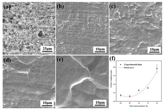
Figure 1.
Surface SEM images of plasma pretreated substrates. Morphologies of plasma pretreated times of (a) 0 h; (b) 0.5 h; (c) 1 h; (d) 1.5 h; and (e) 2 h. (f) Roughness.
The XRD results (Figure 2) reveal that the unpretreated substrate primarily consists of three crystal faces, namely (110), (200), and (211), with the (110) face being the predominant one. However, following the pretreatment of the substrate, there is a decrease in the XRD intensity of the (110) face, accompanied by an enhancement in the prominence of the (200) and (211) faces. This observation suggests that plasma surface treatment not only modifies the surface morphology but also alters the crystal structure, consequently influencing the subsequent coating deposition. The further observation of the diffraction peak corresponding to the (110) crystal face reveals varying degrees of a leftward shift relative to the unpretreated surface, with the degree of deviation increasing as the pretreatment time is prolonged. This phenomenon indicates that the pretreated substrate undergoes expansion in its surface lattice, which can be attributed to the introduction of dislocations and vacancies caused by the bombardment of argon ions on the surface. Further, through calculations, it was determined that the lattice volumes of Ta substrates after 0–2 h of pretreatment were measured as 36.03 Å3, 36.10 Å3, 36.11 Å3, 36.12 Å3, and 36.20 Å3, respectively. As the pretreatment time is extended, the lattice volume exhibited a consistent increasing trend, aligning with the TEM observation results indicating an expansion of surface crystal spacing. This expansion is anticipated to enhance the subsequent atomic diffusion, promoting the formation of a strong metallurgical bond at the interface between the coating and the substrate.
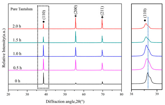
Figure 2.
XRD patterns of the substrate surface for various plasma pretreatment times.
3.2. Microstructure and Adhesion Performance of Coatings
Figure 3 shows the surface morphology of Hf coatings on pretreated Ta substrates for various durations. These coatings exhibit uniform and complete coverage on substrates, whereas the untreated substrate surface displays directional wear scratches. Following the glow plasma pretreatment, the deposited coatings demonstrate a flatter morphology, accompanied by the presence of micro pits and folds that resemble the surface features observed on the pretreated substrate. Interestingly, different from the substrate surface, the surface morphology of the substrate treated for 1.5 h appears to be the most severe among these coatings, rather than the surface treated for 2 h. This may be attributed to the higher surface energy at the step sites, making coating atoms easier to deposit and effectively fill in pitted areas. Strikingly, the coating on the substrate pretreated for 1 h appears to be the flattest surface, closely resembling the characteristics of the untreated substrates. Figure 3f illustrates the average roughness of Hf coatings on different substrates. The coating on the substrate pretreated for 1 h exhibits the lowest roughness value, approximately 0.15 μm, along with the highest level of flatness. In short, the plasma pretreatment on substrates leads to a reduction in the roughness of the following deposited coating as well as an improvement in surface flatness, which can be primarily attributed to the elimination of surface micro scratches.
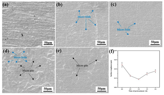
Figure 3.
Surface SEM images of Hf coatings on substrates with various plasma pretreatment times: (a) 0 h; (b) 0.5 h; (c) 1 h; (d) 1.5 h; and (e) 2 h. (f) Roughness.
Figure 4 shows the cross-sectional morphology and EDS results of Hf coatings on pretreated Ta substrates for various durations. The coatings present a uniform and compact structure, devoid of any micro holes or cracks either within the coatings or at the substrate–coating interfaces. The EDS results reveal that the coatings, comprising deposition and interdiffusion layers, exhibit a greater thickness on pretreated substrates. Specifically, the coating obtained on the substrate pretreated for 1 h manifests the utmost thickness of approximately 14 μm, whereby the deposition layer and interdiffusion layer increase to 10 μm and 4 μm, respectively. These outcomes signify that plasma surface pretreatment significantly enhances coating thickness due to the heightened efficiency of atom diffusion, primarily attributed to increased surface defects and elevated surface energy [25].
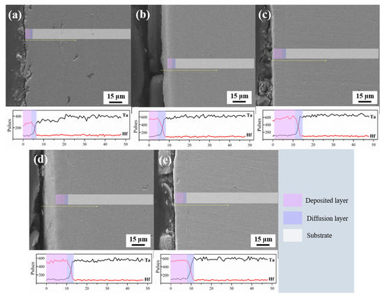
Figure 4.
Cross-section SEM images and EDS results of Hf coatings on substrates with various plasma pretreatment times: (a) 0 h; (b) 0.5 h; (c) 1 h; (d) 1.5 h; and (e) 2 h.
Figure 5 shows the XRD results of Hf coatings on pretreated Ta substrates for various durations. The obtained results reveal that the surface composition of the samples predominantly consists of pure Hf, demonstrating a remarkable preference for the (110) crystal face orientation. Additionally, there is a relatively minor occurrence of Hf (100) and Hf (002) crystal faces within these coatings. Furthermore, the XRD analysis identifies the presence of Ta phases, which diminish in perceptibility with increasing thickness of the Hf coating. These results suggest that the crystal structure of the deposited coatings remains unaffected after the argon plasma surface pretreatment.
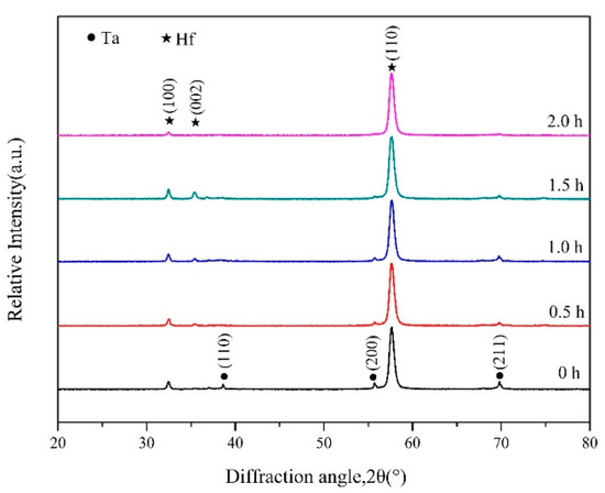
Figure 5.
XRD patterns of Hf coatings on substrates with various plasma pretreatment times.
To meet the diverse requirements of engineering applications, achieving an exceptional bond strength between the coating and the substrate is of utmost importance for the coating. In this study, scratch tests were conducted to evaluate the adhesion performance of the coatings. The scratched scar images with the earliest failure locations marked using arrows and the corresponding acoustic emission spectra are shown in Figure 6. Coatings with arrows shifting to further right locations denote standing higher test pressure in these figures, indicating better adhesion performance. Remarkably, the coating on the substrate pretreated for 1 h exhibits the best adhesion performance, reaching approximately 9.5 N. However, the adhesion value decreases to around 6 N for coatings deposited on substrates pretreated for 1.5 h and 2 h. This decline could be attributed to the crater morphology and pit steps, which increase surface roughness and consequently reduce adhesion performance [8]. In summary, an increase in coating thickness leads to an enhanced ability to withstand positive load, while a smoother coating surface facilitates improved bonding force between the coating and the substrate. It is worth noting that the presence of a diffusion layer significantly enhances the bonding force, and this effect continuously improves with increasing thickness.
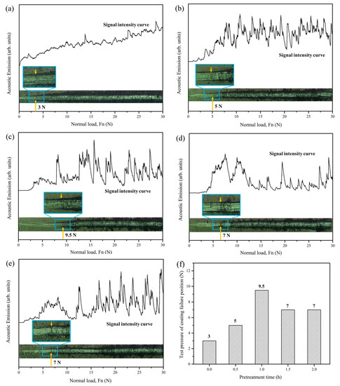
Figure 6.
Scratch tests of Hf coatings on substrates with various plasma pretreatment times: (a) 0 h; (b) 0.5 h; (c) 1 h; (d) 1.5 h; and (e) 2 h. (f) Comparison of the scratch test results.
3.3. TEM Analysis of Coating–Substrate Interface
Figure 7 shows the region near the coating–substrate interface observed from the TEM sample, which was cut using the FIB technique. The comprehensive analysis of morphology and element distribution reveals a composition primarily consisting of Ta and Hf elements. The content of Hf elements gradually decreases from the coating side towards the substrate side, while the Ta content shows the opposite trend, constituting a well-defined continuous gradient structure attributed to mutual element diffusion. Interestingly, a distinctive transition layer is observed at the coating–substrate interface, comprising three different morphologies. Figure 7d provides an enlarged view of Figure 7a marked with a rectangular frame. A refined grain layer can be observed in the Ta substrate, forming a sputtering-affected layer at a depth of approximately 150 nm. The refined grain layer, with grain sizes ranging from 10 to 20 nm, significantly promotes more grain boundaries of high energy, facilitating enhanced element diffusion and thereby improving the interface bonding strength. Figure 7e is selected area electron diffraction (SAED) patterns corresponding to areas circled in Figure 7d, providing a closer examination of the refined grains in the surface layer of the substrate. In addition, although the diffusion transition layer exhibits three different morphologies, it shares the same crystal structure composed of Hf and Ta elements. This discrepancy in appearance can be attributed to variations in the thickness difference during the ion thinning process, resulting in distinct signal reception. Similarly, the bright regions observed in the coating side represent perforations generated during the thinning process. Notably, both the entire diffusion layer and the coating in the visual field consist of nanocrystalline grains with dimensions ranging from 10 to 20 nm, indicating the exceptional mechanical and chemical properties.
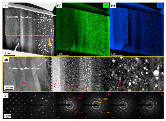
Figure 7.
Cross-section TEM results of Hf coating. (a) Entire morphology; (b) EDS maps of the Hf distribution; (c) EDS maps of the Ta distribution; (d) high-magnification morphology marked in (a); and (e) SAED patterns corresponding to areas circled in (d).
To obtain atomic-scale details of the interface between the coating and the substrate, High-Resolution Transmission Electron Microscopy (HR-TEM) images were captured and are presented in Figure 8. Figure 8b shows a high-magnification image of the internal substrate within the region denoted as box b in Figure 8a. This image is accompanied by the corresponding Fast Fourier Transform (FFT), Inverse Fast Fourier Transform (IFFT), and atomic arrangement images within the same region. An analysis reveals that the single-layer crystal face spacing in the Ta substrate measures 0.238 nm with a well-organized atomic arrangement and no noticeable lattice defects. Figure 8c provides analogous information to Figure 8b but specifically focuses on the sputtering-affected layer of the substrate. It becomes apparent that the sputtering-affected layer exhibits a larger single-layer crystal face spacing of 0.258 nm compared to the internal Ta substrate. Moreover, a significant number of dislocations and vacancies are observed in this region. These high-energy defects are highly conducive to the diffusion of coating atoms into the substrate and their subsequent binding with the substrate atoms [8]. This not only enhances the bonding strength of the coating but also helps to mitigate abrupt changes in the physical and chemical properties resulting from the gradient distribution of the Ta and Hf elements, so that the coating can exhibit significantly heightened dependability and enhanced performance throughout its service cycle. Figure 8d presents a high-magnification image of the coating–substrate interface region. A substantial number of dislocations are evident on the substrate side; concurrently, nanocrystalline and nano-amorphous grains exist on both the interface and coating side. In addition, the continuous gradient structure induces interface fuzziness, thereby promoting enhanced stability in stress release within the coating. Consequently, it effectively mitigates the stress gradient on both sides of the interface arising from structural mutations. These structural features play a pivotal role in enhancing the coating’s toughness, bolstering adhesion, and fortifying its resistance against external damage.
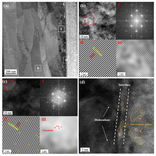
Figure 8.
TEM images (a) near coatings–substrate region; HR-TEM analysis of (b) internal Ta substrate; (c) sputtering-affected layer of Ta substrate; (d) coating–substrate interface.
3.4. First-Principles Calculations
The study suggests that substrate roughness does not have a significant effect on coating thickness [26], and the previous XRD analysis shows a strong change in the substrate crystal face index after plasma surface pretreatment. Consequently, the first-principles calculations were conducted to understand the influence of different crystal faces of the Ta substrate on deposition of Hf coatings in this study. We mainly focused on calculating the formation energies of Hf with Ta on (110), (200), and (211) crystal faces to explain the different performance of coatings. Figure 9 is a computational depicting the combination of Hf atoms with three different crystal faces of Ta.
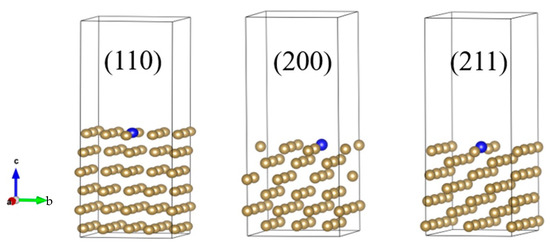
Figure 9.
Computational models of the (a) Ta (110) face, (b) Ta (200) face, and (c) Ta (211) face containing Hf.
Table 1 presents the formation energies of Hf on the three different crystal faces. We calculated the formation energies using the following formula:
where ΔESlab-Hf is the formation energy, ESlab-Hf is the energy of combined slabs, E2Ta is the energy of a single tantalum cell, ESlab is the energy of combined slabs, and E2Hf is the energy of a single hafnium cell.
ΔESlab-Hf = (ESlab-Hf + E2Ta/2) − (Eslab + E2Hf/2)

Table 1.
Formation energies of Hf on the (110), (200), and (211) crystal faces.
The formation energies of Hf on the (110), (200), and (211) crystal faces are −0.25 eV, −0.72 eV, and −0.57 eV, respectively. Compared to the (110) crystal face, the combination energy on the other two crystal faces, particularly the (200) crystal face, is significantly lower, resulting in improved deposition and diffusion efficiency of Hf atoms on the Ta substrate. The article suggests that high-index Ta crystal faces exhibited higher surface energy compared to low-index crystal faces, with values of 1.12 eV/atom of the (110) face, 3.21 eV/atom of the (111) face, and 2.24 eV/atom of the (112) face, respectively [27]. This implies that substrates featuring high-index Ta crystal faces are more favorable for the adsorption of Hf atoms and the deposition of Hf coatings, which aligns with the conclusion drawn in this study.
Figure 10 shows that Hf in the slab of the (200) crystal face has the highest electron energy level, with 3.3 eV−1, which is more than twice that of the (110) crystal face, which has the lowest energy level at 1.3 eV−1. This indicates that Hf atoms can more easily combine with the (200) and (211) crystal faces of Ta [28]. Additionally, the (200) crystal face has the lowest energy level at the Fermi energy among the three Ta slabs, indicating that Hf in the slab of the (200) crystal face has the most stable state. Therefore, the Hf coating can easily combine with the substrate and exist more stably, thereby improving both the thickness and adhesion performance of Hf coatings.
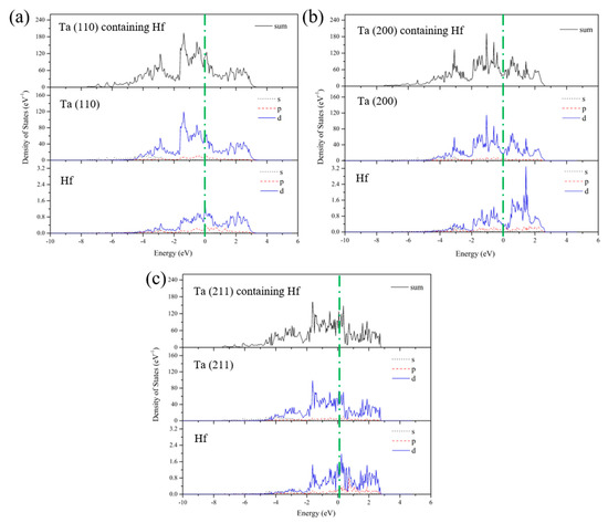
Figure 10.
(a–c) Density of states for Hf, various Ta crystal faces, and various Ta crystal faces containing Hf.
4. Conclusions
In this study, double glow plasma surface metallurgy technology was used to prepare Hf coatings on Ta substrates with various pretreatment times. Conclusions are as follows:
- The plasma surface pretreatment proved to be effective in improving the condition of the substrate surface. It greatly eliminated initial surface micro scratches and enhanced surface flatness. Moreover, the surface pretreatment not only modified the surface morphology of the substrate but also induced changes in the crystal structure of the surface layer. XRD results demonstrated a decrease in the intensity of the Ta (110) face, while the prominence of the Ta (200) and Ta (211) faces became more pronounced.
- The Hf coatings consisted of a deposition layer and diffusion layer, and the glow plasma pretreatment considerably improved the thickness and adhesion performance of the deposited coatings. The coating obtained on the substrate pretreated for 1 h manifested the optimal structure, with a maximum thickness of approximately 14 μm and the best adhesion performance of approximately 9.5 N. The TEM results revealed that the plasma treatment led to grain refinement at a depth of approximately 150 nm. Moreover, the pretreatment resulted in an increase in the crystal face spacing of the substrate as well as high-energy defects, such as vacancies and dislocations. Furthermore, both the diffusion layer and the deposition layer of the coating are exclusively comprised of nanocrystalline grains measuring 10–20 nm in size.
- The crystal defects and lightly increased surface roughness enhance the surface energy, while the Ta (200) and Ta (211) crystal faces, which have a lower combination energy and a more stable state with Hf atoms than the Ta (110) crystal face, are considerably increased on pretreated substrates with a decrease in the Ta (110) crystal face. Because of the high-energy defects and the lower combination energy, the coating elements exhibit enhanced diffusion within the substrate, leading to the better formation of a gradient structure. The gradient structure significantly improved the bonding strength between the substrate and the coating, while simultaneously reducing the stress gradient at both sides of the coating–substrate interface.
Author Contributions
K.Y.: Methodology, Formal analysis, Writing—original draft, Investigation, Supervision. B.D.: Investigation, Writing—original draft, Methodology. X.J.: Data curation, Formal analysis, Writing—original draft. F.L. (Fenghua Lu): Methodology, Formal analysis, Investigation. F.D.: Formal analysis, Funding acquisition. F.L. (Fengkun Li): Investigation, Data curation. D.W.: Writing—original draft. P.Z.: Project administration, Conceptualization, Funding acquisition, Writing—review and editing, Resources. All authors have read and agreed to the published version of the manuscript.
Funding
This work was supported by the Nantong Basic Science Research Program (No. JC12022056).
Data Availability Statement
The datasets generated during and/or analyzed during the current study are available from the corresponding author on reasonable request.
Conflicts of Interest
The authors declare that they have no known competing financial interests or personal relationships that could have appeared to influence the work reported in this paper.
References
- Deng, Y.; Chen, W.; Li, B.; Wang, C.; Kuang, T.; Li, Y. Physical vapor deposition technology for coated cutting tools: A review. Ceram. Int. 2020, 46, 18373–18390. [Google Scholar]
- Ostadi, A.; Hosseini, S.H.; Fordoei, M.E. The effect of temperature and roughness of the substrate surface on the microstructure and adhesion strength of EB-PVD ZrO2-% 8wtY2O3 coating. Ceram. Int. 2020, 46, 2287–2293. [Google Scholar]
- Lugscheider, E.; Bobzin, K. The influence on surface free energy of PVD-coatings. Surf. Coat. Technol. 2001, 142, 755–760. [Google Scholar]
- Morshed, M.M.; McNamara, B.P.; Cameron, D.C.; Hashmi, M.S.J. Effect of surface treatment on the adhesion of DLC film on 316L stainless steel. Surf. Coat. Technol. 2003, 163, 541–545. [Google Scholar]
- Teng, X.; Peng, H.; Li, L.; Guo, H. Investigation on crystal orientations in EB-PVD YSZ coatings under different substrate rotation mode. J. Eur. Ceram. Soc. 2023, 43, 5373–5380. [Google Scholar]
- Sun, W.; Tan, A.W.Y.; Khun, N.W.; Marinescu, I.; Liu, E. Effect of substrate surface condition on fatigue behavior of cold sprayed Ti6Al4V coatings. Surf. Coat. Technol. 2017, 320, 452–457. [Google Scholar]
- Xian, G.; Xiong, J.; Fan, H.; Guo, Z.; Xian, L.; Sun, L.; Zhao, H. Effect of substrate pretreatments on the structure and properties of AlTiN coatings deposited on TiCN-based cermets. Thin Solid Film. 2023, 770, 139769. [Google Scholar]
- Xiao, H.; Liu, X.; Lu, Q.; Hu, T.; Hong, Y.; Li, C.; Zhong, R.; Chen, W. Promoted low-temperature plasma nitriding for improving wear performance of arc-deposited ceramic coatings on Ti6Al4V alloy via shot peening pretreatment. J. Mater. Res. Technol. 2022, 19, 2981–2990. [Google Scholar]
- Zhao, H.; Miao, Q.; Liang, W.; Yi, J.; Liu, R.; Xue, L.; Zuo, S. A study on pre-treatment with rotation accelerated shot peening in multi-NbN films by double glow plasma surface metallurgy. Surf. Coat. Technol. 2021, 405, 126671. [Google Scholar]
- Merisalu, M.; Aarik, L.; Kozlova, J.; Mändar, H.; Tarre, A.; Piirsoo, H.M.; Sammelselg, V. Al alloy protection via ultra-thin ceramic coatings and different surface pretreatments. Surf. Coat. Technol. 2022, 435, 128240. [Google Scholar]
- Zhang, K.; Guo, X.; Wang, C.; Liu, F.; Sun, L. Effect of plasma-assisted laser pretreatment of hard coatings surface on the physical and chemical bonding between PVD soft and hard coatings and its resulting properties. Appl. Surf. Sci. 2020, 509, 145342. [Google Scholar]
- An, S.; Foest, R.; Fricke, K.; Riemer, H.; Fröhlich, M.; Quade, A.; Schäfer, J.; Weltmann, K.; Kersten, H. Pretreatment of cutting tools by plasma electrolytic polishing (PEP) for enhanced adhesion of hard coatings. Surf. Coat. Technol. 2021, 405, 126504. [Google Scholar]
- Huang, H.; Wu, M.C.; Liang, T.; Chen, D.Y.; Tsao, C.C.; Hsu, C.Y. Substrate pretreatment using plasma etching to enhance electroless Ni-P coatings performance. Int. J. Electrochem. Sci. 2020, 15, 7093–7105. [Google Scholar]
- Drábik, M.; Truchlý, M.; Ballo, V.; Roch, T.; Kvetková, L.; Kúš, P. Influence of substrate material and its plasma pretreatment on adhesion and properties of WC/a-C:H nanocomposite coatings deposited at low temperature. Surf. Coat. Technol. 2018, 333, 138–147. [Google Scholar] [CrossRef]
- Xu, Z.; Huang, J.; Wu, H.; Xu, Z.; Liu, X.; Lin, N.; Wei, D.; Zhang, P. A modern-day alchemy: Double glow plasma surface metallurgy technology. AIP Adv. 2022, 12, 030702. [Google Scholar] [CrossRef]
- Chen, X.; Zhang, P.; Wei, D.; Ding, F.; Li, F.; Wei, X.; Ma, S. Preparation and characterization of Cr/CrC multilayer on γ-TiAl alloy by the double glow plasma surface alloying technology. Mater. Lett. 2018, 215, 292–295. [Google Scholar] [CrossRef]
- Qiu, Z.K.; Zhang, P.Z.; Wei, D.B.; Wei, X.F.; Chen, X.H. A study on tribological behavior of double-glow plasma surface alloying W-Mo coating on gear steel. Surf. Coat. Technol. 2015, 278, 92–98. [Google Scholar]
- Rodriguez-Carbajal, J. Recent advances in magnetic structure determination by neutron powder diffraction. Phys. B Condens. Matter. 1993, 192, 55–69. [Google Scholar]
- Rodriguez-Carbajal, J.; Roisnel, T. Line Broadening Analysis Using FullProf*: Determination of Microstructural Properties. Mater. Sci. Forum. 2004, 443, 123–126. [Google Scholar] [CrossRef]
- Klinger, M.; Jager, A. Crystallographic Tool Box (CrysTBox): Automated tools for transmission electron microscopists and crystallographers. J. Appl. Crystallogr. 2015, 48, 2012–2018. [Google Scholar] [CrossRef]
- Perdew, J.P.; Burke, K.; Ernzerhof, M. Generalized gradient approximation made simple. Phys. Rev. Lett. 1996, 77, 3865–3868. [Google Scholar] [CrossRef] [PubMed]
- Kresse, G.; Joubert, D. From ultrasoft pseudopotentials to the projector augmented-wave method. Phys. Rev. B 1999, 59, 1758–1775. [Google Scholar] [CrossRef]
- Kuznetsov, G.V.; Islamova, A.G.; Orlova, E.G.; Ivashutenko, A.S.; Shanenkov, I.I.; Zykov, I.Y.; Feoktistov, D.V. Influence of roughness on polar and dispersed components of surface free energy and wettability properties of copper and steel surfaces. Surf. Coat. Technol. 2021, 422, 127518. [Google Scholar] [CrossRef]
- Tang, L.; Jia, W.; Hu, J. An enhanced rapid plasma nitriding by laser shock peening. Mater. Lett. 2018, 231, 91–93. [Google Scholar] [CrossRef]
- Zhang, C.; Wu, H.; Wang, L.; Yang, X.; Pei, H.; Wei, Y.; Hu, L. Role of the double-glow plasma pre-sputtering in the growth mechanisms and metal–insulator transition of VO2 film. Appl. Surf. Sci. 2022, 603, 154043. [Google Scholar] [CrossRef]
- Huang, R.X.; Qi, Z.B.; Sun, P.; Wang, Z.C.; Wu, C.H. Influence of substrate roughness on structure and mechanical property of TiAlN coating fabricated by cathodic arc evaporation. Phys. Procedia. 2011, 18, 160–167. [Google Scholar] [CrossRef]
- Zhang, Z.; Wang, Q.; Wang, X.; Gao, L. The influence of crystal faces on corrosion behavior of copper surface: First-principle and experiment study. Appl. Surf. Sci. 2017, 396, 746–753. [Google Scholar] [CrossRef]
- Kiejna, A. Surface atomic structure and energetics of tantalum. Surf. Sci. 2005, 598, 276–284. [Google Scholar] [CrossRef]
Disclaimer/Publisher’s Note: The statements, opinions, and data contained in all publications are solely those of the individual author(s) and contributor(s) and not of MDPI and/or the editor(s). MDPI and/or the editor(s) disclaim responsibility for any injury to people or property resulting from any ideas, methods, instructions, or products referred to in the content. |
Disclaimer/Publisher’s Note: The statements, opinions and data contained in all publications are solely those of the individual author(s) and contributor(s) and not of MDPI and/or the editor(s). MDPI and/or the editor(s) disclaim responsibility for any injury to people or property resulting from any ideas, methods, instructions or products referred to in the content. |
© 2023 by the authors. Licensee MDPI, Basel, Switzerland. This article is an open access article distributed under the terms and conditions of the Creative Commons Attribution (CC BY) license (https://creativecommons.org/licenses/by/4.0/).