Article

An Optimized Dip Coating Approach for Metallic, Dielectric, and Semiconducting Nanomaterial-Based Optical Thin Film Fabrication

1
Department of Electronics and Communication Technology, Gauhati University, Guwahati 781014, India
2
Centre of Excellence in Nanotechnology, Assam down town University, Guwahati 781026, India
*
Authors to whom correspondence should be addressed.
Coatings 2023, 13(8), 1391; https://doi.org/10.3390/coatings13081391
Submission received: 18 April 2023 / Revised: 25 July 2023 / Accepted: 26 July 2023 / Published: 8 August 2023
(This article belongs to the Special Issue Recent Advances in Functional Surfaces and Interfaces)

Abstract

:
The field of optical thin films has garnered significant attention due to their potential applications in visible light communication, optical sensing, and imaging. Among the various fabrication methods available, conventional layer-by-layer (LBL) dip coating is less sophisticated and more economical. Nevertheless, this approach frequently encounters deficiencies in the precise control of the growth of thin films. This work aimed at properly comprehending the growth conditions associated with the LBL dip coating process and optimizing the conditions to obtain the best thin film growth for different materials: metallic (Ag), semiconducting (ZnO), and insulating (SiO2). The optimization of the conditions for surface functionalization with 3-aminopropyltriethoxysilane (APTES) together with other parameters like dipping time, drying time, the number of dipping–drying cycles, and the timing of the intermediate APTES layers led to the controlled growth of thin films. Atomic force microscopy and scanning electron microscopy revealed even deposition in the case of ZnO and SiO2 from the very beginning, while with Ag NPs, the growth of the thin film was observed to be uneven and gradually became smooth as the number of layers increased, and a smooth layer could be observed after over 100 layers of dipping.

1. Introduction

Optical thin films or optical filters have become increasingly important in modern technology, finding applications in numerous fields from optical imaging and optical sensing to visible light communications [1,2,3,4,5,6]. One popular method for creating these filters is the fabrication of thin films that can be used to selectively transmit or block certain wavelengths of light [7]. For modern optical filters in the visible and near-infrared (NIR) domain, Fabry–Perot resonating structures [8,9] and free-standing nanostructures at the subwavelength scale [10,11] are used. Fabry–Perot resonating structures are multi-layered thin films with resonant cavities made of heterostructures of plasmonic and dielectric or dielectric and semiconducting materials [8,9]. Free-standing nanostructures are made up of plasmonic materials, dielectric materials, or a heterostructure of plasmonic and dielectric materials [10,11]. The refractive index, which depends on the film material and thickness, maintains the aforementioned optical filter characteristics. A uniform thickness is essential for the performance of these thin films. A uniform thickness ensures that the film’s properties are consistent across the entire surface, allowing for predictable and reproducible behavior. To achieve a uniform thickness, the deposition process must be carefully controlled and optimized [8]. Various deposition techniques including vacuum vapor deposition [12], magnetron sputtering [11,13], and sol–gel deposition [14,15,16] are widely used to fabricate optical thin films. Vacuum vapor deposition [12,13,17] and magnetron sputtering [11] are the techniques commonly used to produce uniform, high-quality films whose thickness and composition may be precisely controlled. However, the major drawback of these techniques is that up-scaling for commercial use is very expensive [11]. Sol–gel deposition is a low-cost, bottom-up approach for the fabrication of thin films that includes the drop casting [9], spin coating [10,17], Langmuir–Blodgett [18], and dip coating techniques [14,17,19,20]. The greatest benefit of sol–gel deposition is that it allows the colloid characteristics to be transferred to the thin film [14,20,21]. However, the limitations of the drop casting [9], spin coating [10], and Langmuir–Blodgett techniques [14] include insufficient control over the film thickness and homogeneity; a dependency on the spinning substrate; and limitations regarding the types of materials that can be used, respectively. In comparison to other sol–gel approaches, the electrostatically self-assembled layer-by-layer (LBL) deposition method via dip coating has fewer limitations and is widely recognized as the preferred technique for producing optical thin films from colloids [14,20,21,22,23,24,25,26,27,28]. Optical thin film fabrication through self-assembled LBL dip coating is widely employed for many applications, such as distributed Bragg reflectors (DBRs) or one-dimensional photonic crystals for electromagnetic spectral manipulation [24], the production of transparent windows that are resistant to fogging and frost [22,23,27], and high-performance optical fiber sensors [22,23,25,26,27]. However, limited knowledge related to the precise control and detailed analysis of thin film growth through the LBL dip coating process is available in the literature [20,29,30]. In this regard, the standardization of the conventional dip coating technique for producing optical thin films from colloids is of utmost importance in order to facilitate the commercialization of these films and fully exploit their potential in diverse applications.
The present study is focused on the development of a single procedure for the production of controlled mono- or heterostructured thin films of metal, semiconductor, and insulator materials to ensure commercial viability. The procedure involved optimizing various conditions affecting thin film growth, such as surface functionalization (using APTES), dipping time, drying time, the number of dipping–drying cycles, and the timing of the intermediate APTES layers. As the process employed here was non-lithographic and non-heating, the properties of the substance being deposited were preserved [28]. Representative materials, viz., Ag as a plasmonic material (both spherical and prismatic), SiO2 as a dielectric material, and ZnO as a semiconducting material, were used in the experiment. Research involving these three materials is important because Ag, SiO2, and ZnO are the most frequently used materials for optical thin film fabrication [2,3,4,14,21,22,23,24,25,26,31,32,33,34]. These materials’ zeta potentials and electrostatic interactions depend on their characteristics. By passivating the nanoparticles’ surfaces with polycation or polyanion molecules, the zeta potential and, subsequently, the electrostatic interaction could be changed [35]. The interaction of the nanoparticles with the quartz substrate, as well as their zeta potential and surface functionalization role, were also studied here. The possibilities of tailoring the zeta potential of colloids with polyanion and polycation molecules open up the pathway for the use of different types of nanoparticles for thin film fabrication.

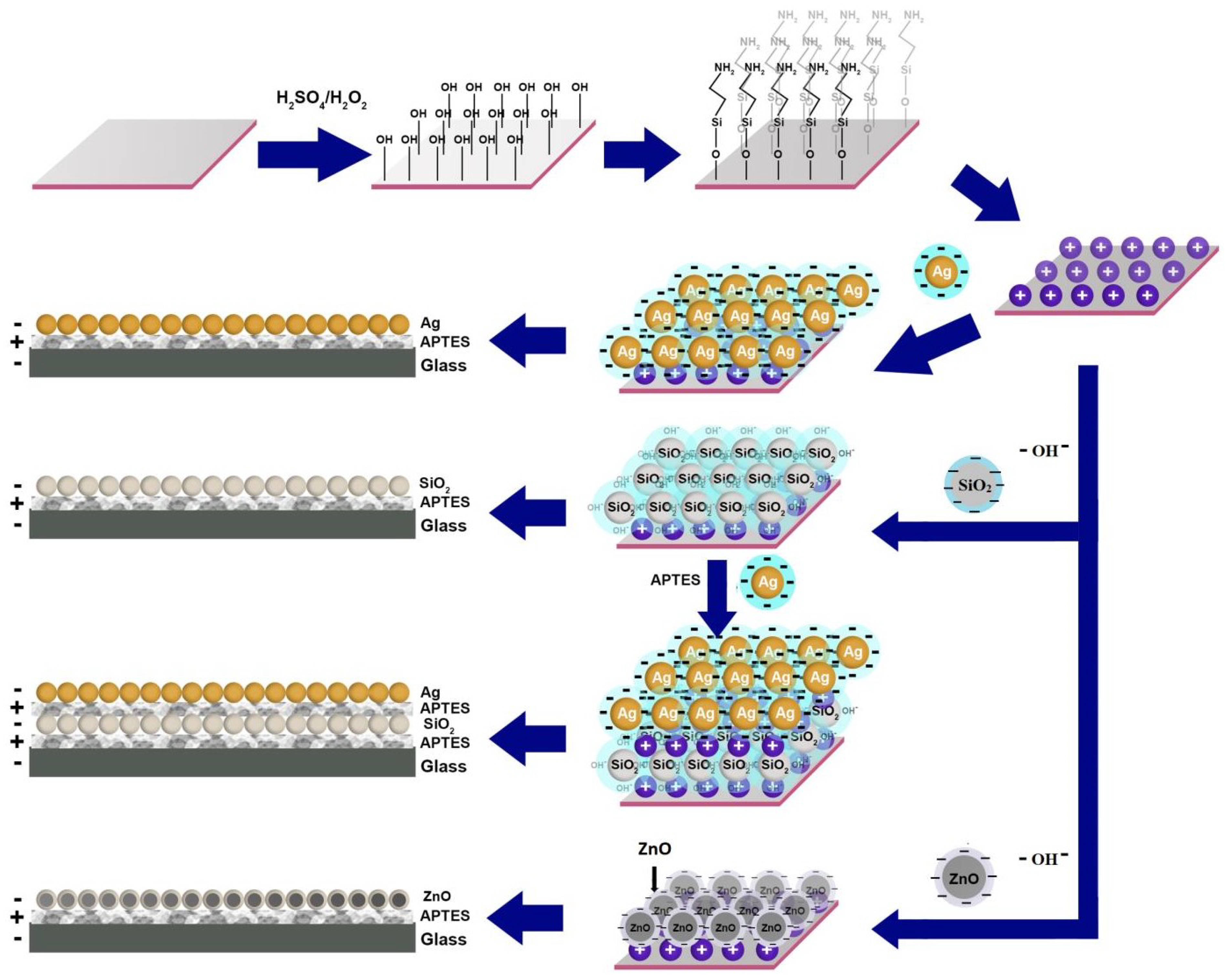
2. Materials and Methods
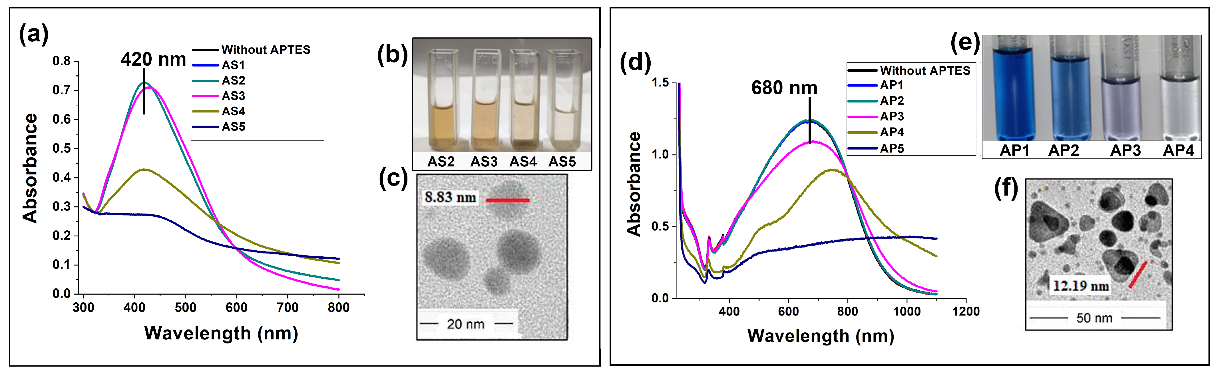
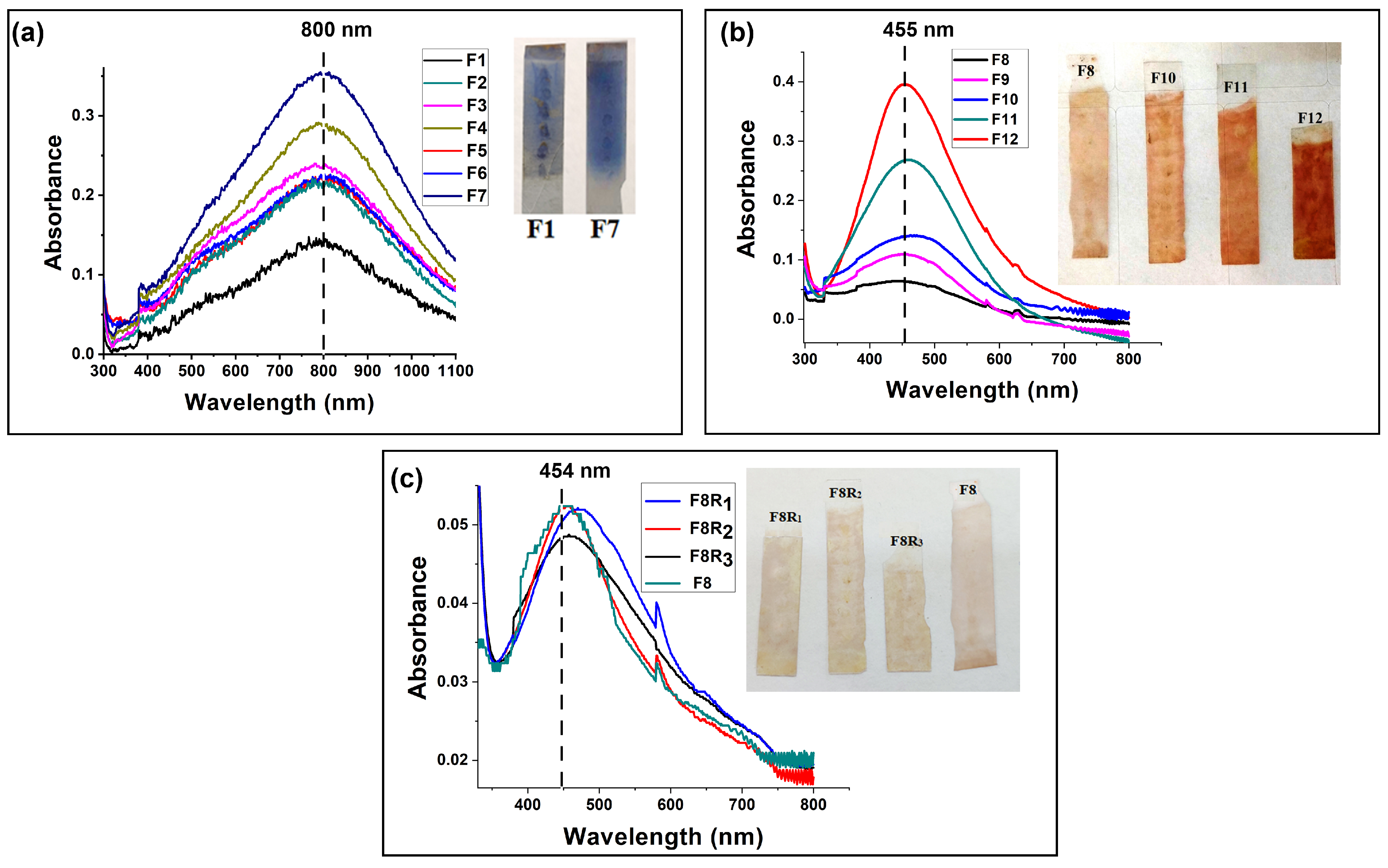
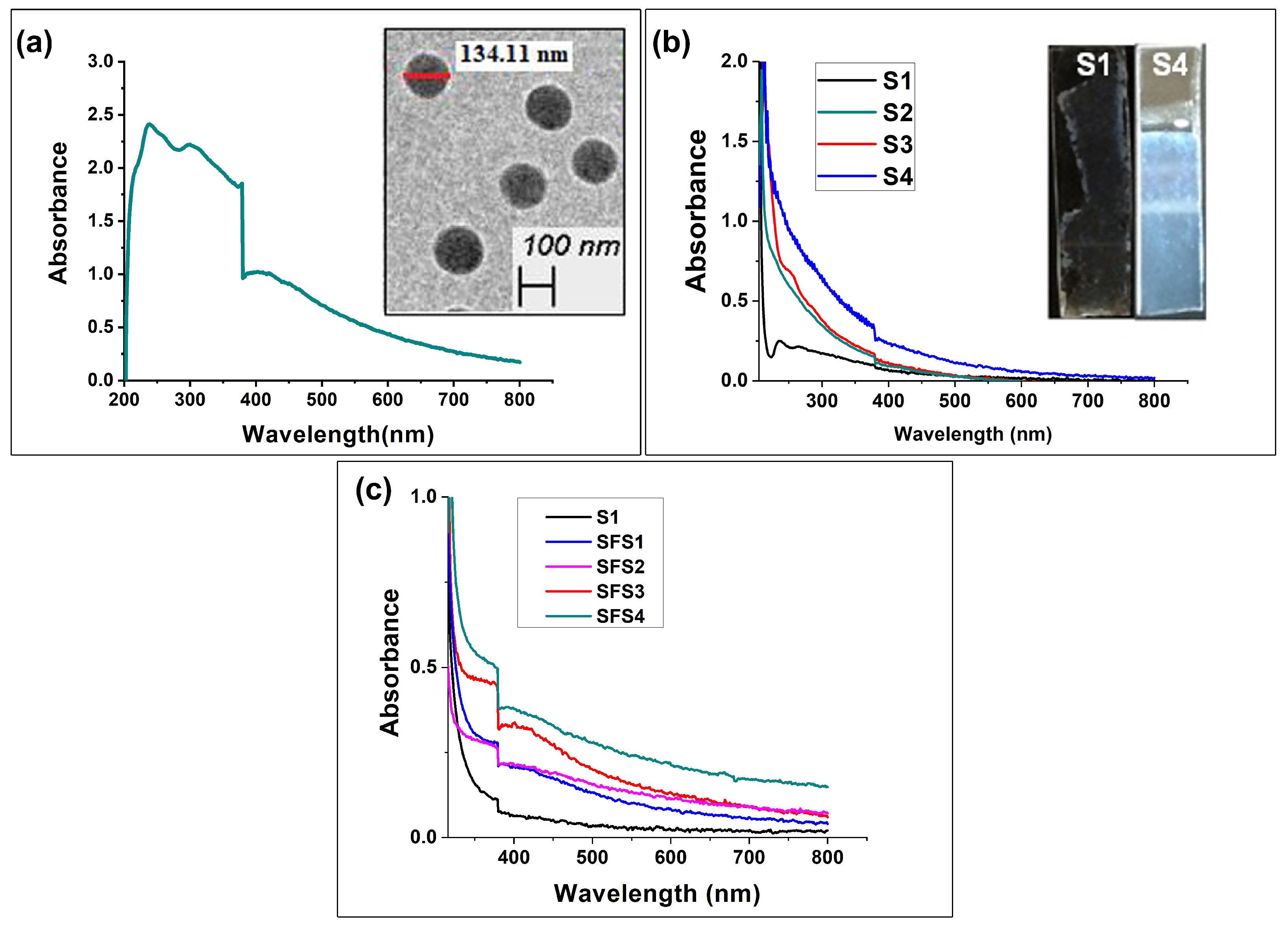
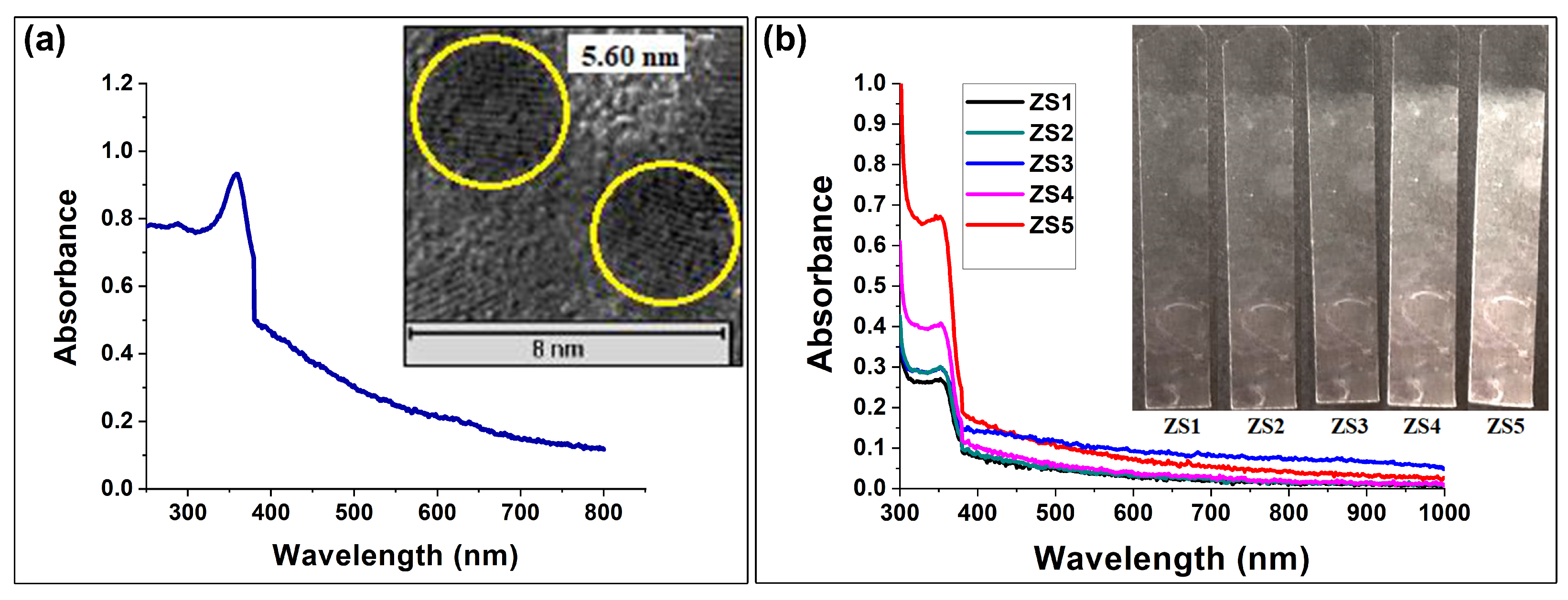
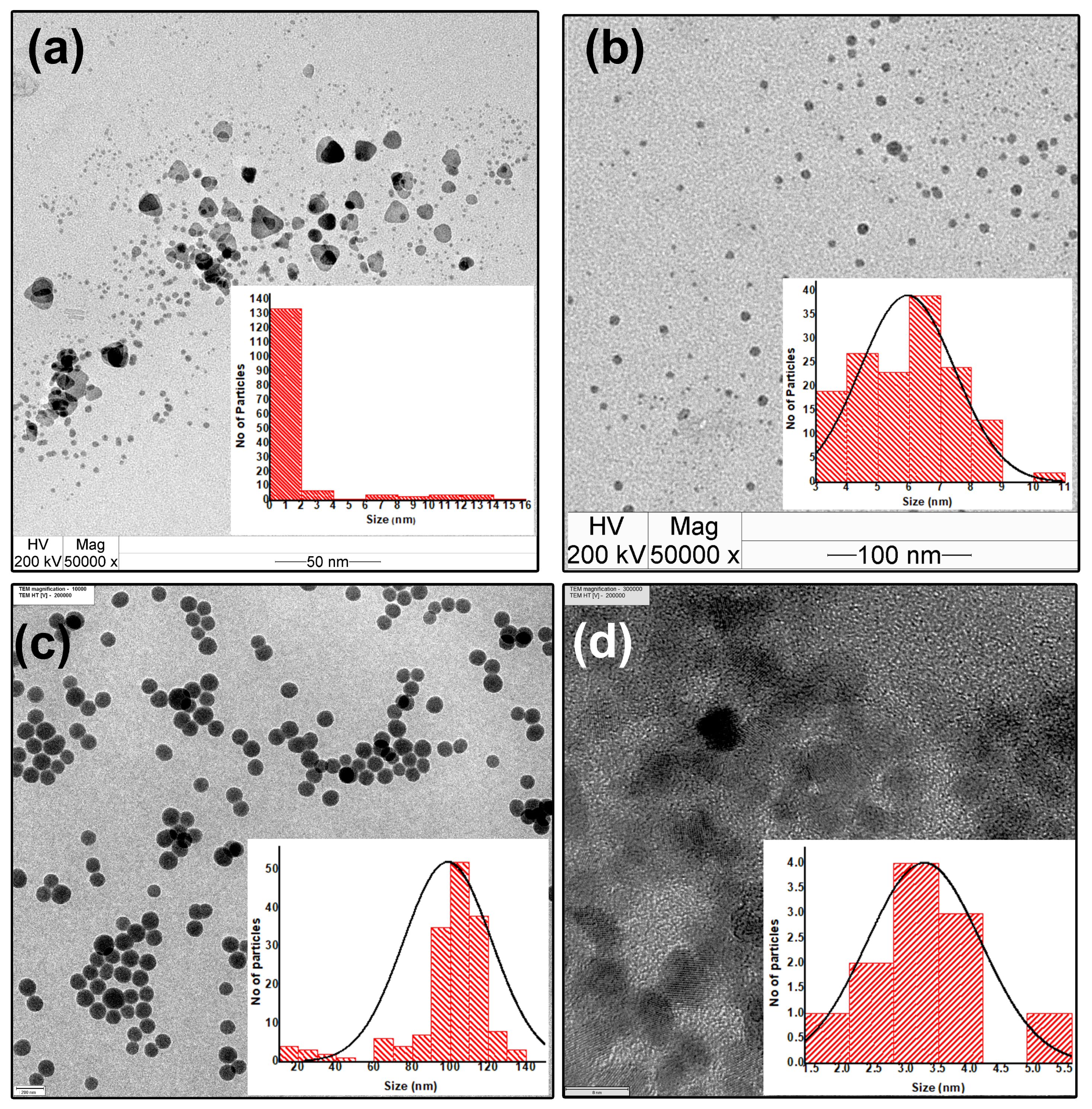
Chemical Reagents: Silver nitrate ((AgNO3), ≥99.9%); trisodium citrate ((Na3C6H5O7), ≥99%); polyvinylpyrrolidone (PVP); hydrogen peroxide ((H2O2), 30%); sodium borohydride ((NaBH4), ≥98%); tetraethyl orthosilicate (TEOS); ammonium hydroxide ((NH4OH), 25%); zinc acetate dihydrate ((Zn(CH3COO)2·2H2O), ≥99%); ethanol ((C2H5OH), ≥99%); and 3-aminopropyltriethoxysilane ((APTES), ≥98.0%) were purchased from Merck (Procured from North East Chemicals Corporation, Guwahati). All samples were prepared by using de-ionized (DI) water.
Synthesis of Ag Nanospheres and Nanosprisms: The one-pot synthesis method proposed by Huang et al. [36] was used for the synthesis of Ag nanospheres and nanoprisms. In this method, 30 mM tri-sodium citrate in 3.68 mL of DI water, 2 w/w% PVP in 3.68 mL of DI water, and 120 μL of hydrogen peroxide were added into the freshly prepared AgNO3 solution (0.14 mM AgNO3 in 43 mL DI water) under continuous stirring. After 3 min, 170 μL and 330 μL of 100 mM NaBH4 were added into the mixtures, which turned light orange and bluish, respectively. Finally, the solutions were kept under cold and dark conditions for stabilization and then observed under UV-vis spectroscopy.
Synthesis of SiO2 Nanoparticles: Based on the SiO2 nanoparticle synthesis used in Natte’s work [37], the Stöber method was used in this study. In order to prepare SiO2 nanoparticles, 250 μL of NH4OH was mixed into 3 mL of absolute ethanol, 125 μL of pure TEOS, and 180 μL of DI water under magnetic stirring that continued at room temperature for 30 min.
Synthesis of ZnO Nanoparticles: Zn(CH3COO)2.2H2O at a 4 mM concentration was prepared in 20 mL ethanol under vigorous stirring at 50 °C for the synthesis of the ZnO nanoparticles. The stirring was continued for 45 min and then diluted with another 20 mL of fresh ethanol. After allowing the solution to cool in air, 20 mL of 4 mM sodium hydroxide in ethanol was added drop by drop while stirring. After 2 h of cooling to room temperature from a temperature of 60 °C, the mixture was analyzed [38].
Thin Film Growth Process using Layer-By-Layer (LBL) Method: The LBL method used for the fabrication of controlled metallic, semiconducting, and dielectric nanoparticle thin films is outlined in Figure 1. Initially, a Piranha-treated [20] quartz plate (immersed in a solution of 30% H2O2 and concentrated H2SO4 in a volume ratio of 7:3 for 30 min under sonication, then washed and dried) was functionalized with APTES solution (20 μL of APTES plus 3.125 mL ethanol); then, the quartz substrate was dipped into the nanoparticle colloid. Finally, dried nanoparticles were deposited on a quartz plate, and we repeated the dipping–drying cycle for multiple deposition steps. After a certain deposition step, the layer growth became saturated. To enhance the layer re-growth, we incorporated the APTES layer at the growth saturation point and repeated steps 4–2, as shown in Figure 1. Similar flows were employed for the fabrication of heterostructured thin films, as shown in Figure 1. The dipping and drying time for all films was 1 min, with the exception of F5 and F6, for which the dipping time was 2 min and 5 min, respectively, while the drying time remained at 1 min. In this study, Ag nanoparticles of two different morphologies were employed for metallic thin films, and ZnO and SiO2 nanoparticles were used for semiconducting and dielectric thin films, respectively. A total of 29 thin films were fabricated in this study, and details of the fabrication of these films are shown in Table 1. The dip coating instrument Xdip SV1 was used to fabricate the thin films.
Characterization: The fabricated thin films were characterized by atomic force microscopy (AFM) (Model: NTEGRA Vita, NTMDT at IASST, Guwahati) and field emission scanning electron microscopy (FE-SEM) (Model:ZEISS Sigma 300 at Chemistry Department, Gauhati University at an acceleration voltage of 3 KV). The size and shape of nanoparticles were characterized by transmission electron microscopy (Model:JEOM 2010 at MTEC, NSTDA, Thailand). The optical characterizations were carried out using an ultraviolet–visible (UV-vis) spectrophotometer (ELICO SL 159 at Assam down town University), and the zeta potential of the nanoparticles was measured by a Malvern Zetasizer at Nanotech, NSTDA, Thailand. All the measurements were taken at room temperature. The details of characterization technique are discussed in Appendix B.

3. Results

In the fabrication of the thin films, APTES was used to functionalize the quartz substrate for the better attachment of the nanoparticles. Before APTES treatment, the Piranha treatment of the quartz substrate was used to generate sites for the attachment of APTES molecules. The amino groups of the APTES molecules were responsible for the positively charged surface of the entire quartz substrate. Hence, the citrate anion on the Ag nanoparticles resulted in strong binding to the positively charged quartz surface and thin film formation. Similarly, the OH ion on the SiO2, as well as ZnO, nanoparticles was the reason for attachment on quartz. The zeta potential and its influence on the formation of monostructured and heterostructured nanoparticle thin films is shown in Figure 2. The effect of the zeta potential of the nanoparticles on the formation of alternative layers is also shown in Figure 2. The zeta potential for ZnO nanoparticles synthesized in ethanol was measured to be −32.6 mV, indicating a stable colloid.
In addition to the significance of the zeta potential of the nanoparticle colloid, it was found that the concentration of APTES, the dipping time, the drying time, the number of dipping–drying cycles, and the timing of the intermediate APTES layer were crucial for the controlled growth of the thin films. Multiple dips of the APTES-functionalized quartz substrate in the same colloid increased the APTES concentration within it, leading to agglomeration and, finally, sedimentation. To optimize the APTES concentration, initially five different volumes of APTES, viz., 10 μL, 20 μL, 30 μL, 40 μL, and 60 μL, were hydrolyzed with 3.125 mL ethanol. It was observed that for APTES concentrations of 20 μL or below 20 μL hydrolyzed with 3.125 mL ethanol, no change occurred in the Ag colloid after 100 dips of the quartz substrates. APTES concentrations above 20 μL hydrolyzed with 3.125 mL ethanol resulted in the agglomeration of nanoparticles and a decrease in absorbance, as shown in Figure 3a,d. Among the different concentrations of APTES, 20 μL of APTES hydrolyzed with 3.125 mL ethanol was found to be the optimum concentration for functionalizing a quartz substrate. The same concentration was found to be optimal for both the spherical and prismatic Ag samples. The sample codes of the Ag nanoparticle colloids after 100 dips of the quartz substrate functionalized at the five abovementioned APTES concentrations (viz., 10 μL, 20 μL, 30 μL, 40 μL, or 60 μL) hydrolyzed with 3.125 mL ethanol were AS1, AS2, AS3, AS4, and AS5 (spherical) and AP1, AP2, AP3, AP4, and AP5 (prismatic). The spherical and prismatic morphologies of the Ag nanoparticles, as well as the size variation, were confirmed from TEM micrographs, as shown in Figure 3c,f.
The timing of the intermediate APTES layer, as well as the optimal dipping and drying times, are depicted in Figure 4a. It was determined that the minimum time for dipping and drying an APTES-functionalized quartz substrate to form an Ag layer was 1 min. Figure 4a reveals that longer dipping times did not significantly contribute to layer growth, as the absorbance of thin films dipped for 1 min, 2 min, and 5 min was nearly identical. However, the number of dipping–drying cycles had a noticeable impact on layer growth: thin film F3 with 100 dipping–drying cycles comprising a 1 min dip and 1 min dry showed better absorbance than F2, F5, and F6 with 50 dipping–drying cycles comprising dipping times of 1 min, 2 min, and 5 min, respectively, and drying times of 1 min for all. With the addition of the APTES layer after 50 dipping–drying cycles, thin film F4 (100 dipping–drying cycles) showed better absorbance as compared to F3 (100 dipping–drying cycles), to which no intermediate APTES layer was applied till 100 cycles; the effect of the APTES layer lasted up to 50 dips and gradually reduced with the number of dips. These results suggest that a 1 min dip, 1 min dry, and the addition of the APTES layer after every 50 dips were the best conditions for metallic thin film growth on a quartz substrate. The results of UV-vis spectroscopy and atomic force microscopy (AFM) characterization shown in Figure 4 and Figure 5, respectively, confirmed that the growth of the Ag thin film increased with an increase in the number of dipping–drying cycle.
The visible change in the color and UV-vis absorbance of thin films F1–F12 shown in Figure 4a,b provides optical confirmation of thin film growth. The surface plasmon resonance (SPR) peaks of thin films F1–F12 confirmed that their morphological variation was nearly identical to that of the colloidal dispersions. Spherical and prismatic Ag colloids had SPR peaks at 420 nm and 680 nm, respectively (shown in Figure 3a,d). The colloids’ thin film SPR peaks were at 455 and 800 nm (Figure 4a,b). The particle size and shape distribution of the synthesized Ag nanoparticles are discussed in Appendix A.1. The thicknesses of thin films F8, F10, and F12 according to the analysis of the AFM results (film thickness = total thickness − bare quartz substrate roughness) were found to be approximately 18.91 nm, 43.8 nm, and 80 nm, respectively (shown in Figure 5a,d,e). From the AFM images, it could also be concluded that the morphology of the thin films gradually smoothened with the increase in dipping cycles. As shown in Figure 5h, the root-mean-square (RMS) roughness of the thin films showed a decreasing trend in accordance with the increasing dipping iterations (details of the roughness parameters are discussed in Appendix A.2). The AFM results were also validated by SEM micrographs for the F10 thin film, as shown in Figure 5f. Consistency in the thickness of thin films for multiple repetitions of the same growth parameters is essential to standardize a thin film growth procedure. To find consistency, the thin film growth parameters for F8 were repeated three additional times on the quartz substrate, and the respective UV-vis and AFM results were analyzed. Thin films F8, F8R1, F8R2, and F8R3 showed similarity in absorbance as well as in morphology (as shown in Figure 4c and Figure 5a,b,c). From AFM analysis, thin films F8, F8R2, and F8R3 showed near-similar thicknesses, i.e., approximately 18.91 nm, 18.41 nm, and 17.9 nm, respectively. Based on the AFM micrographs of thin films F8, F10, and F12, the increasing trend and empirical formula for thin film thickness in accordance with the number of dipping–drying cycles are shown in Figure 5g.
The procedure followed for developing the metallic thin film was kept similar to that for the development of the dielectric thin film. The APTES concentration to functionalize the quartz substrate was kept the same. As SiO2 nanoparticles are much larger than Ag nanoparticles (as shown in Figure 3c,f and Figure 6a), the number of dipping–drying cycles and the timing of intermediate APTES layers were changed, as given in Table 1. The average diameters of the spherical Ag nanoparticles and SiO2 nanoparticles were, respectively, 6.0 ± 3.0 nm and 105.0 ± 15 nm. The average length and height of the prism-shaped nanoparticles were 9.0 ± 3.0 nm and 12.0 ± 2.0 nm, respectively (thoroughly discussed in Appendix A.1). As shown in Figure 6, the absorbance enhancement was significant for steps S1 to S2 and S2 to S4, but steps S2 to S3 had a very low absorbance enhancement. This was because no intermediate APTES layer was used for S2 to S3. The timing of the intermediate APTES layers was optimized by incorporation after each dipping–drying cycle. The changes in layer growth in accordance with the number of dipping–drying cycles were also confirmed through the SEM micrographs shown in Figure 7. The side-view SEM images of the SiO2 thin films were analyzed to estimate the film thicknesses. Thin film S1, with a single instance of dipping, produced a monolayer of SiO2 nanoparticles (with a film thickness of around 131.5 nm). Thin films S2 and S4 had thicknesses around 293.6 nm and 850.8 nm, respectively. Figure 7f displays the empirical formula and the increasing trend (based on the SEM micrographs of S1, S2, and S4) for the relationship between the number of dipping–drying cycles and the thin film thickness of SiO2 nanoparticles. The quantitative element analysis of thin film S4 was carried out through SEM-EDX characterization, as shown in Figure 7d, confirming its SiO2 composition (the maximum percentage availability of Si and O compared to the other elements).
The development of metallic/dielectric heterostructured thin films was achieved through the alternate dipping of Ag and SiO2 nanoparticles and the incorporation of the APTES layer after every single dipping of SiO2 and every 50 dippings of Ag, respectively. A visible change in UV-vis absorbance for the alternate deposition of Ag and SiO2 confirmed the heterostructured thin film growth shown in Figure 6c. The cross-sectional view of the SEM micrographs and SEM-EDX for the SFS3 thin film shown in Figure 7e confirmed the alternate SiO2 and Ag layer growth.
The synthesized ZnO nanoparticles were similar in size (as shown in Figure 8a) to the Ag nanoparticles, so the same steps used to create the metallic thin films were also employed to create the ZnO thin films (fabrication details are given in Table 1). The average diameter of the ZnO nanoparticles was 3.37 ± 2.1 nm (thoroughly discussed in Appendix A.1). Similar to the Ag nanoparticle deposition, the timing of the intermediate APTES layers for the ZnO nanoparticle thin films was optimized to occur after every 50 dipping–drying cycles. The absorbance enhancement was lower without the intermediate APTES layers (as shown in Figure 8b). Thin films ZS1, ZS4, and ZS5 exhibited substantial changes in absorbance and morphology as a function of the number of dipping–drying cycles, as depicted in Figure 8b and Figure 9. The thicknesses of the ZnO nanoparticle thin films were estimated by analyzing the side views of the SEM micrographs. The thicknesses of thin films SZ1, SZ4, and SZ5 were approximately 360.8 nm, 426.69 nm, and 850.8 nm, respectively.
Based on the SEM micrographs of thin films ZS1, ZS4, and ZS5, the empirical formula and the increasing trend for the relationship between the number of dipping–drying cycles and the thin film thickness are shown in Figure 9d. The SEM-EDX characterization of the ZnO thin film’s composition (maximum percentage of Zn and O availability) is shown in Figure 9c.

4. Conclusions

The optimization of the parameters involved in the conventional dip coating approach for the fabrication of optical thin films was carried out under precise control. The parameters, viz., the surface functionalization (using varied APTES concentrations), dipping time, drying time, number of dipping–drying cycles, and timing of the intermediate APTES layers, were optimized for the effective growth of thin films, which was confirmed through AFM and SEM characterization. The best surface affixation was observed for Ag using a mixture of APTES and ethanol in the ratio of 1:156 by volume of as-purchased chemicals (20 μL APTES hydrolyzed with 3.125 mL ethanol). Depending upon the requirements, different parameters can be opted for. The particle sizes used for the growth of insulating and semiconductor thin films were on average 134.11 nm for SiO2 nanoparticles and 5.60 nm for ZnO nanoparticles. Measurements carried out on the SEM micrographs of the thin films revealed particle sizes comparable to the original colloidal form, indicating minimal agglomeration during the deposition process. The comparable absorbance peaks observed in the thin films of the corresponding Ag colloids also indicated minimal agglomeration during deposition for Ag thin films. The AFM micrographs confirmed that the metallic (Ag) nanoparticle-deposited thin films (F8, F8R2, and F8R3) showed high surface roughness in the initial layers and gradually smoothened according to the increasing number of dips (after 100 layers). All the fabricated thin films showed an increasing polynomial trend in thickness. Optimizing the system by adjusting the aforementioned variables paves the way for the development of fully automated thin film fabrication systems.

Author Contributions

Conceptualization, A.K.S.; methodology, A.K.S. and S.B.; software, A.K.S. and D.S.; validation, A.K.S. and S.B.; formal analysis, A.K.S. and S.B.; investigation, A.K.S. and D.S.; resources, A.K.S.; data curation, A.K.S. and D.S.; writing—original draft preparation, A.K.S. and D.S.; writing—review and editing, A.K.S., D.S., P.D. and S.B.; visualization, A.K.S. and S.B.; supervision, P.D. and S.B. All authors have read and agreed to the published version of the manuscript.

Funding

This research received no external funding.

Institutional Review Board Statement

Not applicable.

Informed Consent Statement

Not applicable.

Data Availability Statement

Data sharing is not applicable to this article.

Acknowledgments

The authors acknowledge the support provided by Gauhati University and Assam Downtown University through granting access to their laboratory and instrumentation facility.

Conflicts of Interest

The authors declare no conflict of interest.

Abbreviations

The following abbreviations are used in this manuscript:
viz.Videlicet
SEMScanning electron microscopy
TEMTransmission electron microscopy
UV-visUltraviolet-visible spectroscopy
APTES3-aminopropyltriethoxysilane
NPsNanoparticles
SPRSurface plasmon resonance
AFMAtomic force microscopy

Appendix A

Appendix A.1

In the process of synthesizing prismatic Ag nanoparticles, small Ag nanoparticles ranging from 1 to 2 nm were formed. The percentage of these small nanoparticles was 82%, and only 2.8% of the nanoparticles had a prismatic shape. The average length and height of the prism-shaped nanoparticles were 9.0 ± 3.0 nm and 12.0 ± 2.0 nm, respectively (as shown in Figure A2a). During the synthesis of spherical Ag nanoparticles, a significant majority of the particles exhibited a spherical morphology, as depicted in Figure A2b. The average diameter of these spherical nanoparticles was 6.0 ± 3.0 nm. The process employed in the synthesis of SiO2 and ZnO nanoparticles resulted in the generation of nanoparticles with average diameters of 105.0 ± 15.0 nm and 3.37 ± 2.1 nm, respectively, as illustrated in Figure A2c,d.

Appendix A.2

The AFM micrographs confirmed that the metallic (Ag) nanoparticle-deposited thin films (F8, F8R2, and F8R3) showed high surface roughness in the initial layers and gradually smoothened according to the increasing number of dips (after 100 layers). Thin film F8 at 25 layers had a root-mean-square (RMS) roughness of 14.27 nm, whereas thin film F10 at 100 layers had an RMS roughness of 10.04 nm, and thin film F12 at 150 layers had an RMS roughness of 6.59 nm. Figure A1a–c depict the RMS roughness of thin films F8, F10, and F12, respectively. The aforementioned results showed a decreasing trend in surface roughness in accordance with an increasing number of dipping iterations.

Appendix B

The details of the characterization techniques and sample preparation are presented below.
Scanning electron microscopy (SEM) was carried out to determine the width of the thin films using a ZEISS Sigma 300 field emission scanning electron microscope maintained at an acceleration voltage of 3 KV. In order to image the thin films using a scanning electron microscope (SEM), the thin films were first cleaned using an air blower before being placed into a sputter coater for gold coating, which was required to prevent charge accumulation on the specimen surface. The thickness of the gold coating was maintained at around 5 nm such that the coating was thick enough to prevent charging but not thick enough to obscure specimen surface details. After gold coating, the specimen was inserted into the SEM chamber, where a high-energy electron beam was guided by the condenser lenses to generate a concentrated electron probe on the specimen. This probe had a diameter ranging from approximately 0.4 nm to 5 nm. In order to deflect the beam across the surface of the sample, the beam was directed through sets of deflection coils. When the electron beam struck the sample, it was scattered and absorbed randomly, thereby losing energy. During the period of interaction, there was an exchange of energy between the electron beam and the specimen. This exchange generated high-energy backscattered electrons. These backscattered electrons were subsequently detected and translated into digital images based on the sample’s surface topography. Thus, the specimen’s signal intensity determined the image. Transmission electron microscopy (TEM) was carried out to determine the size of the synthesized nanoparticles using a JEOL/JEM 2010 TEM operated at 200 kV. For the TEM imaging sample preparation, the nanoparticle colloid was diluted considerably (at least 10 times) to ensure the detection of dispersed particles. A carbon-coated TEM copper grid was placed on a glass slide and covered with a drop of nanoparticle colloid. The grid was then left for a few minutes, placed on filter paper, and allowed to dry at room temperature. Following the completion of sample preparation, the prepared samples were introduced into the TEM, where a beam of electrons interacted with an ultra-thin sample and transmitted through it. This interaction allowed for the observation of the crystal structure, composition, and defects within the sample. The outcome of this interaction led to the formation of an image, which was subsequently amplified and directed toward an imaging apparatus, such as a fluorescent screen, a layer of photographic film, or a CCD camera. The capacity to visualize the target is a thousand times greater in TEM compared to optical microscopy, as the process of imaging uses a smaller wavelength of electron beam instead of light. As a result, detailed information on the internal structures can be analyzed.
Atomic force microscopy (AFM) was carried out to determine the morphology of the thin films using an NTEGRA Vita NTMDT AFM with a scanning size of 2.0 × 2.0 μm2. In order to scan the surface topography of the sample and obtain the width of the thin film on the quartz substrate, the substrate was initially inserted into the AFM, where a cantilever with a sharp tip (radius 10 nm) scanned the sample surface in semi-contact mode. In the semi-contact or tapping mode, the tip periodically made contact with or tapped the surface of the sample. This was facilitated by the use of a piezoelectric crystal that caused the cantilever to oscillate in a vertical direction near its resonance frequency. The resonance frequency was set at 1 Hz to scan the fabricated thin films’ surfaces. A feedback system was responsible for ensuring the constancy of the oscillation amplitude. When the tip traversed a depression on the surface, the cantilever experienced expanded space for oscillation, resulting in increased amplitude. Likewise, the magnitude of the amplitude diminished as the tip traversed a raised surface. The utilization of alterations in oscillation amplitude served as a means to identify and quantify surface characteristics.

References

  1. Căilean, A.M.; Dimian, M. Current challenges for visible light communications usage in vehicle applications: A survey. IEEE Commun. Surv. Tutor. 2017, 19, 2681–2703. [Google Scholar] [CrossRef]
  2. Pimenta, S.; Cardoso, S.; Miranda, A.; De Beule, P.; Castanheira, E.; Minas, G. Design and fabrication of SiO2/TiO2 and MgO/TiO2 based high selective optical filters for diffuse reflectance and fluorescence signals extraction. Biomed. Opt. Express 2015, 6, 3084–3098. [Google Scholar] [CrossRef] [Green Version]
  3. Kim, D.; Woo, H.K.; Lee, Y.M.; Kim, Y.; Choi, J.H.; Oh, S.J. Controllable doping and passivation of ZnO thin films by surface chemistry modification to design low-cost and high-performance thin film transistors. Appl. Surf. Sci. 2020, 509, 145289. [Google Scholar] [CrossRef]
  4. Yu, R.; Mazumder, P.; Borrelli, N.F.; Carrilero, A.; Ghosh, D.S.; Maniyara, R.A.; Baker, D.; García de Abajo, F.J.; Pruneri, V. Structural coloring of glass using dewetted nanoparticles and ultrathin films of metals. ACS Photonics 2016, 3, 1194–1201. [Google Scholar] [CrossRef] [Green Version]
  5. Shaukat, A.; Noble, F.; Arif, K.M. Nanostructured color filters: A review of recent developments. Nanomaterials 2020, 10, 1554. [Google Scholar] [CrossRef]
  6. Ge, P.; Liang, X.; Wang, J.; Zhao, C.; Gao, X.; Ding, Z. Optical filter designs for multi-color visible light communication. IEEE Trans. Commun. 2018, 67, 2173–2187. [Google Scholar] [CrossRef]
  7. Kaiser, N. Review of the fundamentals of thin-film growth. Appl. Opt. 2002, 41, 3053–3060. [Google Scholar] [CrossRef] [PubMed]
  8. Barber, Z.; Blamire, M. High throughput thin film materials science. Mater. Sci. Technol. 2008, 24, 757–770. [Google Scholar] [CrossRef]
  9. Kumar, A.K.S.; Zhang, Y.; Li, D.; Compton, R.G. A mini-review: How reliable is the drop casting technique? Electrochem. Commun. 2020, 121, 106867. [Google Scholar] [CrossRef]
  10. Mustafa, H.A.M.; Jameel, D.A. Modeling and the main stages of spin coating process: A review. J. Appl. Sci. Technol. Trends 2021, 2, 91–95. [Google Scholar] [CrossRef]
  11. Safi, I. Recent aspects concerning DC reactive magnetron sputtering of thin films: A review. Surf. Coat. Technol. 2000, 127, 203–218. [Google Scholar] [CrossRef]
  12. Affinito, J.; Martin, P.; Gross, M.; Coronado, C.; Greenwell, E. Vacuum deposited polymer/metal multilayer films for optical application. Thin Solid Film. 1995, 270, 43–48. [Google Scholar] [CrossRef]
  13. Wasa, K.; Kanno, I.; Kotera, H. Handbook of Sputter Deposition Technology: Fundamentals and Applications for Functional Thin Films, Nano-Materials and MEMS; William Andrew Publishing: Norwich, NY, USA, 2012. [Google Scholar]
  14. Khan, Z.R.; Khan, M.S.; Zulfequar, M.; Khan, M.S. Optical and structural properties of ZnO thin films fabricated by sol-gel method. Mater. Sci. Appl. 2011, 2, 340–345. [Google Scholar] [CrossRef] [Green Version]
  15. Tian, W.; Vahid Mohammadi, A.; Wang, Z.; Ouyang, L.; Beidaghi, M.; Hamedi, M.M. Layer-by-layer self-assembly of pillared two-dimensional multilayers. Nat. Commun. 2019, 10, 2558. [Google Scholar] [CrossRef] [Green Version]
  16. Suchikova, Y.; Kovachov, S.; Bohdanov, I.; Popova, E.; Moskina, A.; Popov, A. Characterization of CdxTeyOz/CdS/ZnO Heterostructures Synthesized by the SILAR Method. Coatings 2023, 13, 639. [Google Scholar] [CrossRef]
  17. Butt, M.A. Thin-film coating methods: A successful marriage of high-quality and cost-effectiveness—A brief exploration. Coatings 2022, 12, 1115. [Google Scholar] [CrossRef]
  18. Samha, H.; DeArmond, M.K. Multilayer sol-gel films using the Langmuir-Blodgett deposition method. Langmuir 1993, 9, 1927–1929. [Google Scholar] [CrossRef]
  19. Kitsomboonloha, R.; Ngambenjawong, C.; Mohammed, W.; Chaudhari, M.; Hornyak, G.; Dutta, J. Plasmon resonance tuning of gold and silver nanoparticle-insulator multilayered composite structures for optical filters. Micro Nano Lett. 2011, 6, 342–344. [Google Scholar] [CrossRef]
  20. Higashi, N.; Takagi, T.; Koga, T. Layer-by-layer fabrication of well-packed gold nanoparticle assemblies guided by a β-sheet peptide network. Polym. J. 2010, 42, 95–99. [Google Scholar] [CrossRef] [Green Version]
  21. Rivero, P.J.; Goicoechea, J.; Matias, I.R.; Arregui, F.J. A comparative study of two different approaches for the incorporation of silver nanoparticles into layer-by-layer films. Nanoscale Res. Lett. 2014, 9, 301. [Google Scholar] [CrossRef] [Green Version]
  22. Rivero, P.J.; Goicoechea, J.; Arregui, F.J. Layer-by-layer nano-assembly: A powerful tool for optical fiber sensing applications. Sensors 2019, 19, 683. [Google Scholar] [CrossRef] [Green Version]
  23. Rivero, P.J.; Urrutia, A.; Goicoechea, J.; Arregui, F. Optical fiber humidity sensors based on Localized Surface Plasmon Resonance (LSPR) and Lossy-mode resonance (LMR) in overlays loaded with silver nanoparticles. Sens. Actuator B Chem. 2012, 173, 244–249. [Google Scholar] [CrossRef]
  24. Yuehui, W.; Xing, Y. High-reflection optical thin films based on SiO2/TiO2 nanoparticles multilayers by dip coating. Micro Nano Lett. 2018, 13, 1349–1351. [Google Scholar] [CrossRef]
  25. Shibraen, M.H.; Yagoub, H.; Zhang, X.; Xu, J.; Yang, S. Anti-fogging and anti-frosting behaviors of layer-by-layer assembled cellulose derivative thin film. Appl. Surf. Sci. 2016, 370, 1–5. [Google Scholar] [CrossRef]
  26. Saffar, M.A.; Eshaghi, A.; Dehnavi, M.R. Fabrication of superhydrophobic, self-cleaning and anti-icing ZnO/PTFE-SiO2 nano-composite thin film. Mater. Chem. Phys. 2021, 259, 124085. [Google Scholar] [CrossRef]
  27. Rivero, P.J.; Urrutia, A.; Goicoechea, J.; Matias, I.; Arregui, F. A Lossy Mode Resonance optical sensor using silver nanoparticles-loaded films for monitoring human breathing. Sens. Actuator B Chem. 2013, 187, 40–44. [Google Scholar] [CrossRef]
  28. Michel, M.; Toniazzo, V.; Ruch, D.; Ball, V. Deposition mechanisms in layer-by-layer or step-by-step deposition methods: From elastic and impermeable films to soft membranes with ion exchange properties. ISRN Mater. Sci. 2012, 2012, 701695. [Google Scholar] [CrossRef] [Green Version]
  29. Scherino, L.; Giaquinto, M.; Micco, A.; Aliberti, A.; Bobeico, E.; La Ferrara, V.; Ruvo, M.; Ricciardi, A.; Cusano, A. A time-efficient dip coating technique for the deposition of microgels onto the optical fiber tip. Fibers 2018, 6, 72. [Google Scholar] [CrossRef] [Green Version]
  30. Wu, L.; Yang, D.; Fei, L.; Huang, Y.; Wu, F.; Sun, Y.; Shi, J.; Xiang, Y. Dip-coating process engineering and performance optimization for three-state electrochromic devices. Nanoscale Res. Lett. 2017, 12, 390. [Google Scholar] [CrossRef] [PubMed]
  31. Eshaghi, A.; Aghaei, A.A.; Zabolian, H.; Jannesari, M.; Firoozifar, A. Transparent superhydrophilic SiO2/TiO2/SiO2 tri-layer nanostructured antifogging thin film. Ceram. Silik. 2013, 57, 210–214. [Google Scholar]
  32. Szeghalmi, A.; Helgert, M.; Brunner, R.; Heyroth, F.; Gösele, U.; Knez, M. Atomic layer deposition of Al2O3 and TiO2 multilayers for applications as bandpass filters and antireflection coatings. Appl. Opt. 2009, 48, 1727–1732. [Google Scholar] [CrossRef] [PubMed]
  33. Shelemin, A.; Baloukas, B.; Zabeida, O.; Klemberg-Sapieha, J.E.; Martinu, L. Fabrication of plasmonic Ag nanoparticles for optical coating applications. In Proceedings of the Optical Interference Coatings Conference (OIC 2022), Whistler, BC, Canada, 19–24 June 2022; Optica Publishing Group: Washington, DC, USA, 2022; p. MD-3. [Google Scholar]
  34. Park, C.; Kim, T.; Kim, Y.I.; Lee, M.W.; An, S.; Yoon, S.S. Supersonically sprayed transparent flexible multifunctional composites for self-cleaning, anti-icing, anti-fogging, and anti-bacterial applications. Compos. Part B Eng. 2021, 222, 109070. [Google Scholar] [CrossRef]
  35. Halbus, A.F.; Horozov, T.S.; Paunov, V.N. Surface-modified zinc oxide nanoparticles for antialgal and antiyeast applications. ACS Appl. Nano Mater. 2020, 3, 440–451. [Google Scholar] [CrossRef] [Green Version]
  36. Huang, T.; Xu, X.H.N. Synthesis and characterization of tunable rainbow colored colloidal silver nanoparticles using single-nanoparticle plasmonic microscopy and spectroscopy. J. Mater. Chem. 2010, 20, 9867–9876. [Google Scholar] [CrossRef] [Green Version]
  37. Natte, K.; Behnke, T.; Orts-Gil, G.; Würth, C.; Friedrich, J.F.; Österle, W.; Resch-Genger, U. Synthesis and characterisation of highly fluorescent core–shell nanoparticles based on Alexa dyes. J. Nanopart. Res. 2012, 14, 680. [Google Scholar] [CrossRef]
  38. Baruah, S.; Rafique, R.F.; Dutta, J. Visible light photocatalysis by tailoring crystal defects in zinc oxide nanostructures. Nano 2008, 3, 399–407. [Google Scholar] [CrossRef]
Figure 1. Thin film growth process by LBL method.
Coatings 13 01391 g001
Figure 2. Zeta potential of nanoparticles and their influence on the formation of alternative layers.
Coatings 13 01391 g002
Figure 3. Optimization of APTES concentration: (a) UV-vis absorption spectra for spherical Ag nanoparticles after 100 dips of the quartz substrate functionalized at different APTES concentrations; (b) optical image to visualize the effect of different concentrations of APTES on spherical Ag NPs; (c) TEM micrographs of spherical Ag nanoparticles; (d) UV-vis absorption spectra for prism-shaped Ag nanoparticles after 100 dips of the quartz substrate functionalized at different APTES concentrations; (e) optical image to visualize the effect of different concentration of APTES on prism-shaped Ag NPs; (f) TEM micrographs of prism-shaped Ag nanoparticles.
Coatings 13 01391 g003
Figure 4. UV-vis absorption spectra of (a) Ag nanoparticle (prism-shaped) thin film growth for different numbers of dipping–drying cycles and optical image of the same; (b) Ag nanoparticle (spherical) thin film growth at different numbers of dipping–drying cycles and optical image of the same; (c) repeatability of the thin films for the same dipping parameters.
Coatings 13 01391 g004
Figure 5. AFM micrographs of (a) thin film F8, (b) thin film F8R2, (c) thin film F8R3, (d) thin film F10, (e) thin film F12, (f) SEM micrographs for thin film F10, (g) thin film thickness of Ag nanoparticles as a function of number of dipping–drying cycles (the data for thin film thickness used in the graph were the average of 3 sets of corresponding thin films), (h) RMS roughness of Ag thin film as a function of number of dips.
Coatings 13 01391 g005
Figure 6. UV-vis absorption spectra of (a) SiO2 nanoparticles along with TEM micrographs; (b) SiO2 nanoparticle-deposited thin films for different numbers of dipping–drying cycles; (c) SiO2/Ag nanoparticle-deposited heterostructured thin films.
Coatings 13 01391 g006
Figure 7. SEM results of (a) thin film S1, (b) thin film S2, (c) thin film S4, (d) SEM-EDX results for thin film S3, (e) SEM and SEM-EDX results for SiO2/Ag heterostructured thin film, (f) thin film thickness of SiO2 nanoparticles as a function of number of dipping–drying cycles (the data for thin film thickness used in the graph were the average of 3 sets of corresponding thin films).
Coatings 13 01391 g007
Figure 8. UV-vis spectroscopy of (a) ZnO nanoparticles (with TEM results where yellow circles represent the diameter of the nanoparticles) and (b) thin film growth at different numbers of dipping–drying cycles.
Coatings 13 01391 g008
Figure 9. SEM results for (a) thin film ZS3 and (b) thin film ZS5, (c) SEM-EDX results for thin film ZS4, (d) SEM-EDX results for ZnO thin film (the data for thin film thickness used in the graph were the average of 3 sets of corresponding thin films).
Coatings 13 01391 g009
Figure A1. SEM results for (a) thin film ZS3 and (b) thin film ZS5; (c) SEM-EDX results for thin film ZS4, (d) SEM-EDX results for ZnO thin film (the data for thin film thickness used in the graph were the average of 3 sets of corresponding thin films).
Coatings 13 01391 g0a1
Figure A2. AFM micrographs and surface roughness of (a) thin film F8, (b) thin film F10, and (c) thin film F12.
Coatings 13 01391 g0a2
Table 1. Experimental parameters for fabrication of thin films.
Thin FilmDepositing NanoparticlesNo. of DipsTiming of Intermediate APTES Layer
F1Ag (prismatic)25-
F250-
F3100-
F4100After 50 dipping–drying cycles
F550 *-
F6100 *-
F7150After every 50 dipping–drying cycles
F8Ag (spherical)25-
F935-
F1050-
F11100After 50 dipping–drying cycles
F12150After every 50 dipping–drying cycles
3-4 F8R1 25-
F8R2 25-
F8R3 25-
S1SiO21-
S22After the first dip
S33
S44After every dipping–drying cycle
SFS1Both SiO2 and Ag (spherical)Silica-1Silica—after every dipping–drying cycle
Ag-50
SFS2Silica-2
Ag-50
SFS3Silica-2Ag—after every 50 dipping–drying cycles
Ag-100
SFS4Silica-3
Ag-100
ZS1ZnO50-
ZS2100-
ZS3150-
ZS4100After 50 dipping–drying cycles
ZS5150After every 50 dipping–drying cycles
* The dipping and drying times for all thin films were 1 min, with the exception of F5 and F6, for which the dipping times were 2 min and 5 min, respectively, while the drying time remained at 1 min.
Disclaimer/Publisher’s Note: The statements, opinions and data contained in all publications are solely those of the individual author(s) and contributor(s) and not of MDPI and/or the editor(s). MDPI and/or the editor(s) disclaim responsibility for any injury to people or property resulting from any ideas, methods, instructions or products referred to in the content.

