Abstract
The characterization of defect states in a hydrothermally grown single crystal of ZnO was performed using deep-level transient spectroscopy in the temperature range of 77–340 K. The native intrinsic defect energy level within the ZnO band gap occurred in the depletion region of ZnO Schottky barrier diodes. A major defect level was observed, with a thermal activation energy of 0.27 eV (E3) within the defect state distribution from 0.1 to 0.57 eV below the conduction band minimum. We confirmed the maximum defect concentration to be 3.66 × 1016 cm−3 at 0.27 eV (E3). As a result, we clearly confirmed the distribution of density of defect states in the ZnO band gap.
1. Introduction
Zinc oxide has attracted a lot of interest recently, due to its direct and wide band gap (3.4 eV at 300 K), high mobility, and simple processing, which make it suitable for optical applications such as light-emitting diodes (LEDs), and as a channel material for thin-film transistors (TFTs) in flat-panel displays [1,2,3,4]. While ZnO has a great deal of potential as a candidate for many optical applications, the electrical role of native defects in ZnO (e.g., Zn interstitial (Zni), Zn vacancy (VZn) and oxygen vacancy (V0)) still remains unclear. It is also difficult to control the electrical defect properties and understand the exact mechanisms of carrier transport, which are associated with a complex defect distribution [5]. Native defects could extensively affect the electrical and optical properties of ZnO-based electronic devices. In particular, the role of defect distribution has been widely examined using photoluminescence (PL) [6], electron paramagnetic resonance (EPR) [7], admittance spectroscopy (AS) [8], and deep level transient spectroscopy (DLTS) [9,10,11,12].
Among these techniques, DLTS has a high sensitivity and is suitable for the analysis of defect states and impurities using Schottky diodes or p–n junction devices [13]. Therefore, the electronic defect states of ZnO have been intensively investigated using DLTS to find the evidence of intrinsic conductivity and the role of defect states. One of the most dominant defect states in n-type ZnO is the well-known V0 due to the relatively low formation energy of 3.5 eV. Recently, V0 has turned out to be a deep donor rather than a shallow donor [5]. Therefore, the origin of intrinsic n-type conductivity in undoped ZnO is believed not to be V0. However, there is not a consensus regarding the source of the intrinsic n-type conductivity in undoped ZnO. Moreover, the explicit role of the defect states has not been fully explained, especially regarding the defect state distribution.
Up to now, very few papers have addressed the identity of defect states [9,14,15]. Additionally, none of these have confirmed the defect state distribution within the ZnO band gap. In this work, we have clearly confirmed the defect state distribution under the conduction band minimum (CBM) in the ZnO band gap. A summary of the prominent defect properties observed in ZnO using DLTS is shown in Table 1, compared with our result in the end row. In our method, we applied boiling H2O2 (prior to metal deposition) on the Zn-face (0001) of hydrothermally grown single-crystal ZnO, with Pd Schottky contacts to improve the Schottky contacts [8,16,17,18,19]. DLTS measurements were employed to investigate the defect state distribution. Defect energy levels with E3 (0.27–0.30 eV) and E4 (0.53 eV) in the ZnO Schottky barrier diodes (SBDs) have been confirmed in previous literature [20,21,22,23]. The major defect state of E3 (0.27 eV) below the CBM was also observed in our Pd/ZnO SBDs from the variations of the transient capacitance slope.

Table 1.
Literature survey of the electronic properties of prominent defects investigated by deep level transient spectroscopy (DLTS) in as-grown ZnO; the defect energy level (Et), defect concentration (Nt), capture cross section (σn) and oxygen vacancy (V0).
2. Experimental Methods
A hydrothermally grown single crystal of bulk ZnO with the (0001) Zn face up was used in this experiment. The Zn face has a lower amount of surface defect concentrations than the O face, which allows for a higher Schottky barrier height [18]. The carrier concentration, mobility, and resistivity of ZnO were measured at 0.86 × 1017 cm−3, 91.9 cm2·V−1·s−1, and 0.85 Ω·cm, respectively, through Hall effect measurements using the van der Pauw geometry (sample size of 10 × 10 × 5 mm3).
The samples were cleaned in an ultrasonic bath with acetone, isopropyl alcohol (IPA), and de-ionized (DI) H2O, sequentially. Before the metallization, the samples were placed into a boiling solution of 30% H2O2 for 3 min to improve the quality of the Schottky contacts, based on previous reports [8,19,23], and were blown using N2 gas. As shown in Figure 1, annular ohmic contacts (inside diameter = 550 μm, outside diameter = 800 μm) and Schottky contacts (diameter 450 μm) were formed on the ZnO surface via electron-beam evaporation (base pressure of ~10−6 mbar) and lift-off photolithography. Ti/Al/Pt/Au (20/80/40/80 nm) and Pd (60 nm) were deposited as ohmic and Schottky contacts, respectively [24]. The samples were then annealed at 200 °C for 1 min under an N2 atmosphere. The Schottky contact area was 1.59 × 10⁻³ cm2.
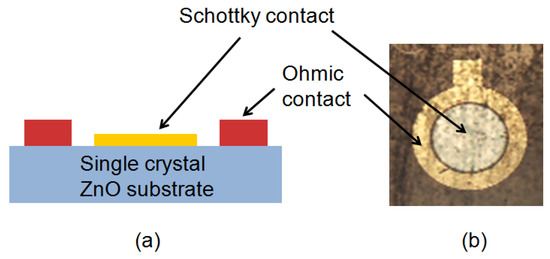
Figure 1.
(Color Online) Simplified schematic illustration of the Pd/ZnO Schottky Barrier Diode (SBD): (a) Cross sectional view, (b) Top view (optical microscope image). Pd and Ti/Al/Pt/Au are used as Schottky and ohmic contacts, respectively.
Current–voltage (I–V), capacitance–voltage (C–V), and DLTS measurements were performed on the Pd/ZnO SBDs. The I–V and C–V measurements were carried out in the dark at room temperature using an Agilent 4156C Precision Semiconductor Parameter Analyzer, and an Agilent E4980A LCR meter. For the C–V measurement, the bias voltage was applied from 0 to −3 V, at 1 MHz. The measurement and data extraction of the DLTS (FT1030 DLTS, PhysTech GmbH, Moosburg, Germany) were followed in a previous report [13].
3. Results and Discussion
Figure 2 shows the I–V curve of the Pd/ZnO SBD. In order to form improved Schottky contacts on ZnO, a Schottky metal contact (e.g., Au, Ag, Pt, and Pd) on ZnO is required. However, the Schottky contact behavior of ZnO does not follow the work function difference directly due to unexpected surface defect states [5,16,17]. To overcome this problem, several techniques have been applied to the ZnO surface, such as oxygen plasma treatment, organic solvent cleaning and hydrogen peroxide (H2O2) treatment [8,18]. Among these treatments, the H2O2 treatment led to the surface defects of ZnO being significantly eliminated and the Schottky contacts between ZnO and metal being improved [8,19].
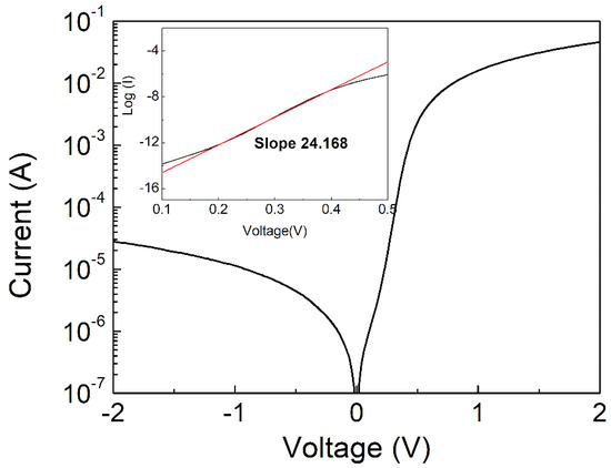
Figure 2.
(Color Online) I–V characteristics of the Pd/ZnO SBDs from -3 to 2 V at room temperature. Ideality factor (n) is shown in the inset.
The leakage current was 2.8 × 10⁻⁵ A with a reverse bias of -2.5 V at room temperature. The leakage current was rectified over 103, and reached 4.61 × 10⁻² A at 2 V. Rectifying behavior was clearly shown in the Pd/ZnO SBDs. Typically, the calculation of the Schottky barrier height in diodes can be conducted using both I–V and C–V techniques, which are important to evaluate the diode performance. To calculate the Schottky barrier height in our devices, the saturation current (Is) can be applied to the following equation [25]:
where A, A*, and ØB represent the Schottky contact area (0.00159 cm2), the effective Richardson constant, and the Schottky barrier height, respectively. The theoretical value of A* in ZnO is 32 A·cm−2·K−2 based on an effective mass (m*) of 0.27m0 [5]. The barrier height is calculated from Is (1.6 × 10⁻⁷ A) at a zero bias from Equation (1). Is was determined by extrapolating the curve of ln[I/(1−exp(−qV/kT))] versus voltage under a forward bias up to V = 0 V. The calculated ØB of our device was 0.85 eV, consistent with previous reports [18].
The ideality factor (n) is plotted by using the ln[I/(1−exp(−qV/kT))] versus voltage curve as shown in the inset of Figure 2, and n is extracted from the slope of this curve for the evaluation of the diode performance [25]. The current–voltage relationship for a Schottky diode can be expressed as I = Io[exp(qV/nkT)−1] ≈ Io *exp(qV/nkT), and gives ln(I) = ln(Io)+qV/nkT. Therefore, in this plot of ln(I) vs. V, the slope ( can be extracted, and the ideality factor is calculated using the below equation. Here, we extracted the value of 1.49 in the linear region. This could be attributed to the carrier recombination, tunneling, or the interfacial layer between the metal and the semiconductor [5,26].
Figure 3 shows the C–V characteristics of the Pd/ZnO SBDs. We considered two factors, with built-in potential (Vbi) and carrier concentration (Nd) evaluated as follows: an approximate evaluation of Vbi was obtained using the intercept of the 1/C2 versus voltage plot, and Nd was also calculated from the slope of this plot (a). Nd was obtained using 2/(qεεoa), where q, ε, and εo represent the elementary charge, the static dielectric constant (8.5 for ZnO), and the vacuum permittivity, respectively [25]. The calculated Vbi of the Pd/ZnO SBDs was 0.77 eV. Moreover, the carrier concentration of ZnO is 2.0 × 1017 cm−3, which is similar to the value obtained using Hall effect measurements (0.86 × 1017 cm−3). The Schottky barrier height was in turn obtained using the following equation [25]:
where Nc is the effective density of states of ZnO in the conduction band (2.94 × 1018 cm−3 using Nc = 2(2πm*kT/h2)3/2). The ØB of our Pd/ZnO SBDs turned out to be 0.863 eV. The values of the Schottky barrier height showed very similar results, regardless of the measurement methods, which indicates that the Pd Schottky contact on ZnO was formed successfully. The detailed Schottky properties of the Pd/ZnO SBDs are listed in Table 2.
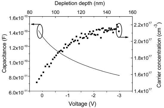
Figure 3.
C–V characteristics of the Pd/ZnO SBDs as a function of reverse bias at 1 MHz. Carrier concentration versus depletion width is also plotted.
Table 2.
The extracted parameters of the Pd/ZnO SBDs at room temperature: the ideality factor (n), reverse current (Irev), barrier heights (ØB), built-in voltage (Vbi) and carrier density (Nd).
For the defect analysis of ZnO, we carried out DLTS measurements for the different temperature ranges from 77 to 340 K at a frequency of 1 MHz. Applied reverse bias voltage was used at −2.5 V to form of a strong depletion region and forward bias voltage was then applied at 0 V with a filling pulse time width (tp) of 50 ms, as shown in Figure 4a. The transient capacitance was measured to within 40 ms at different temperatures from 77 to 340 K (corresponding to 0.1–0.57 eV below the conduction band (Ec)). The maximum transient capacitances were extracted by using different emission rates (en) (emission rate = ln(t1/t2)/(t2–t1), where t1 and t2 are the start and end of the time window), and emission rates of 0.034, 0.042, 0.093, 0.423, and 0.888 ms−1 were selected as shown in Figure 4b. In addition, emission rates (en) can also be determined using the equation below [25]:
with γn = (νth/T1/2)(Nc/T3/2) = 3.25 × 10²¹ (mn/mO) cm−2·s−1·K−2, where mn is the electron density of-states effective mass and mO is the electron rest mass. At different settings of t1 and t2, the DLTS signal gave out a different set of emission rates for the different temperatures. By using an Arrhenius plot of ln (en/T2) vs. 1/T, the trap energy level (Et) and capture cross-section (σn) were obtained. The Arrhenius plot had a slope of −(Ec−Et)/K, determining Et, and an intercept on the ln (en/T2) axis of ln (γnσn), determining σn. We calculated the defect energy level (Et) and capture cross section (σn) by using the Arrhenius plot as shown in Figure 4c. Therefore, we confirmed that the Et and σn of ZnO were Ec–0.27 eV (labeled E3) and 1.36 × 10⁻¹⁶ cm2, respectively [9,20]. It is well known that ZnO has various defect energy levels originating from non-stoichiometry (e.g., Zni, VZn, Oxygen antisite (OZn or V0), etc.) [27,28,29,30].
en/T2 = γnσn × exp(−((Ec−Et)/KT))
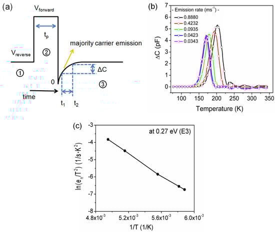
Figure 4.
(Color online) (a) Applied voltage and resultant transient capacitance; (b) DLTS spectra of the Pd/ZnO SBDs samples under different emission rates from 0.0343 ms−1 (t1 = 20.2 ms, t2 = 40.4 ms) to 0.8880 ms−1 (t1 = 0.78 ms, t2 = 1.56 ms); (c) Arrhenius plot of the level E3.
This transient capacitance behavior may have been caused by the positively charged defects through the thermal emission of carriers in the depletion region, and by decreased depletion width due to the increase in total charge density, as shown in Figure 5a–c. This is because the donor-type defect is positively ionized when it is unoccupied and neutral when it is filled with an electron [25]. In this manner, the signal gives out a different set of emission rates and temperatures. The trap emits carriers at this emission rate. As a result, transient capacitance was increased. This phenomenon is in agreement with those obtained from previous reports [27,31]. However, the origin of these defects is still unclear and complex. It requires further study to find the precise evidence of the defect formation.
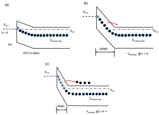
Figure 5.
(Color online) A Schottky diode for majority carrier emission; (a) zero bias (forward bias), (b) reverse bias at t = 0, (c) reverse bias as t → ∞.
Typically, both interface and bulk-trap states can contribute to the DLTS signal in a Schottky junction. Although it was difficult to extract only the bulk traps, due to the overlapping of the electron emissions from the interface states (~1014 cm−2), the interface state density was much weaker than that of the bulk defect states (~1017 cm−3) [32]. Therefore, the predominant defect formation could be defined within the bulk ZnO. Based on DLTS of the Pd/ZnO SBDs, we clearly observed the change of the transient capacitance from 77 to 340 K and predicted the defect states’ distribution between 0.1 and 0.57 eV below the CBM.
The DLTS signal reflects the distribution of the signal originated from each defect energy level. Hence, the DLTS signal is simply proportional to the defect concentration (Nt) given by the equation [13,25]:
where Nd, ΔCmax, and C0 represent the carrier concentration, maximum transient capacitance amplitude, and capacitance of the device at −2.5 V (C0 = 85 pF), respectively. The temperature range from 77 to 340 K can also be related to the defect energy level from 0.1 to 0.57 eV below the CBM, and the defect distribution can be calculated by the electron emission rate equation [13,25,30,33]:
where kT, σn, νth, and τ0 represent the thermal energy, electron capture cross-section area of the trap (assumed to be 10−16 cm2), electron thermal velocity, and emission time constant approximated to be half of the time width used in the measurements (τ0 = 20 ms), respectively [33]. Calculated defect concentration and distribution are shown in Figure 6. Scattering and noise within the data seemed to be due to thermal instability. We confirmed the maximum defect concentration to be 3.66 × 1016 cm−3 at 0.27 eV from the CBM.
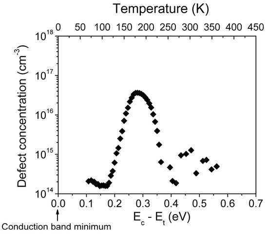
Figure 6.
(Color online) The correspondent subgap density of states as a function of defect energy from the conduction band.
4. Conclusions
We investigated single-crystal ZnO SBDs and carried out a DLTS analysis to find the defect state distribution in the ZnO band gap. We confirmed that a Schottky barrier height of 0.85 eV with a Pd contact was formed on the Pd/ZnO SBDs. Compared to previous reports, our ZnO SBDs have a similar defect energy level of Ec–0.27 eV below the CBM. Although the origin of defects is still unclear and more studies are needed, we believe that complex oxygen-related defects could possibly be the source of defects near the conduction band of single crystal ZnO (in the Pd/ZnO SBDs). Finally, we successfully obtained a defect state distribution below the conduction band in the range of 0.1–0.57 eV. The maximum defect concentration was 3.66 × 1016 cm−3, 0.27 eV from the CBM.
Author Contributions
Conceptualization, writing, and experiments J.P. and Y.S.R.; methodology and analysis, P.S., J.W.; supervision and editing, D.S. All authors have read and agreed to the published version of the manuscript.
Funding
Financial support was provided by the University of California, Los Angeles (UCLA) school of engineering, Samsung, and Basic Science Research Program through the National Research Foundation of Korea (NRF), funded by the Ministry of Education (2017R1D1A1B03030818).
Acknowledgments
J.H. Park and Y.S. Rim equally contributed to this work. Financial support was provided by the University of California, Los Angeles (UCLA) school of engineering and Samsung. We would also like to thank the Nanoelectronics Research Facility (NRF), acknowledge the use of the Integrated Systems Nanofabrication Cleanroom (ISNC) at the California NanoSystems Institute (CNSI) in UCLA, and thank the Basic Science Research Program through the National Research Foundation of Korea (NRF), funded by the Ministry of Education (2017R1D1A1B03030818), for making the fabrication of this device possible. Special thanks to Alan Farrell and Diana Huffaker for their support.
Conflicts of Interest
The authors declare no conflict of interest.
References
- Jagadish, C.; Pearton, S.J. Zinc Oxide Bulk, Thin Films and Nanostructures: Processing, Properties, and Applications, 1st ed.; Elsevier: Oxford, UK, 2006. [Google Scholar]
- Wager, J.F. Transparent electronics. Science 2003, 300, 1245–1246. [Google Scholar] [CrossRef]
- Fortunato, E.; Barquinha, P.; Pimentel, A.; Goncalves, A.; Marques, A.; Pereira, L.; Martins, R. ACMBG Pi-mentel, AMF Goncalves, AJS Marques and LMN Pereira. Adv. Mater. 2005, 17, 590. [Google Scholar] [CrossRef]
- Monakhov, E.V.; Kuznetsov, A.Y.; Svensson, B.G. Zinc oxide: Bulk growth, role of hydrogen and Schottky diodes. J. Phys. D: Appl. Phys. 2009, 42, 153001. [Google Scholar] [CrossRef]
- Özgür, Ü.; Alivov, Y.I.; Liu, C.; Teke, A.; Reshchikov, M.A.; Doğan, S.; Avrutin, V.; Cho, S.J.; Morkoç, H. A comprehensive review of ZnO materials and devices. J. Appl. Phys. 2005, 98, 041301. [Google Scholar] [CrossRef]
- Zeuner, A.; Alves, H.; Hofmann, D.M.; Meyer, B.K.; Heuken, M.; Bläsing, J.; Krost, A. Structural and optical properties of epitaxial and bulk ZnO. Appl. Phys. Lett. 2002, 80, 2078. [Google Scholar] [CrossRef]
- Hofmann, D.M.; Hofstaetter, A.; Leiter, F.; Zhou, H.; Henecker, F.; Meyer, B.K.; Orlinskii, S.B.; Schmidt, J.; Baranov, P.G. Hydrogen: A relevant shallow donor in zinc oxide. Phys. Rev. Lett. 2002, 88, 045504. [Google Scholar] [CrossRef]
- Schifano, R.; Monakhov, E.V.; Grossner, U.; Svensson, B.G. Electrical characteristics of palladium Schottky contacts to hydrogen peroxide treated hydrothermally grown ZnO. Appl. Phys. Lett. 2007, 91, 193507. [Google Scholar] [CrossRef]
- Scheffler, L.; Kolkovsky, V.I.; Lavrov, E.V.; Weber, J. Deep level transient spectroscopy studies of n-type ZnO single crystals grown by different techniques. J. Phys.: Condens. Matter 2011, 23, 334208. [Google Scholar] [CrossRef]
- Chicot, G.; Muret, P.; Santailler, J.-L.; Feuillet, G.; Pernot, J. Oxygen vacancy and EC− 1 eV electron trap in ZnO. J. Phys. D: Appl. Phys. 2014, 47, 465103. [Google Scholar] [CrossRef]
- Gür, E.; Coşkun, C.; Tüzemen, S. High energy electron irradiation effects on electrical properties of Au/n-ZnO Schottky diodes. J. Phys. D: Appl. Phys. 2008, 41, 105301. [Google Scholar] [CrossRef]
- Ohbuchi, Y.; Kawahara, T.; Okamoto, Y. Morimoto, Distributions of Interface States and Bulk Traps in ZnO Varistors. J. Jpn. J. Appl. Phys. 2011, 40, 213. [Google Scholar] [CrossRef]
- Lang, D.V. Fast capacitance transient appartus: Application to ZnO and O centers in GaP p-n junctions. J. Appl. Phys. 1974, 45, 3023. [Google Scholar] [CrossRef]
- Auret, F.D.; Goodman, S.A.; Hayes, M.; Legodi, M.J.; Laarhoven, H.A.V.; Look, D.C. The influence of high energy proton bombardment on the electrical and defect properties of single-crystal ZnO. J. Phys.: Condens. Matter. 2001, 13, 8989. [Google Scholar]
- Rucavado, E.; Jeangr, Q.; Urban, D.F.; Holovský, J.; Remes, Z.; Duchamp, M.; Landucci, F.; Dunin-Borkowski, R.E.; Körner, W.; Elsässer, C.; et al. Enhancing the optoelectronic properties of amorphous zinc tin oxide by subgap defect passivation: A theoretical and experimental demonstration. Phys. Rev. B 2017, 95, 245204. [Google Scholar] [CrossRef]
- Sheng, H.; Muthukumar, S.; Emanetoglu, N.W.; Lu, Y. Schottky diode with Ag on (1120) epitaxial ZnO film. Appl. Phys. Lett. 2002, 80, 2132. [Google Scholar] [CrossRef]
- Allen, M.W.; Alkaisi, M.M.; Durbin, S.M. Metal Schottky diodes on Zn-polar and O-polar bulk ZnO. Appl. Phys. Lett. 2006, 89, 103520. [Google Scholar] [CrossRef]
- Brillson, L.J.; Lu, Y. ZnO Schottky barriers and Ohmic contacts. J. Appl. Phys. 2011, 109, 121301. [Google Scholar] [CrossRef]
- Schifano, R.; Monakhov, E.V.; Svensson, B.G.; Diplas, S. Surface passivation and interface reactions induced by hydrogen peroxide treatment of n-type ZnO (000 1). Appl. Phys. Lett. 2009, 94, 132101. [Google Scholar] [CrossRef]
- Fang, Z.-Q.; Claflin, B.; Look, D.C.; Dong, Y.F.; Mosbacker, H.L.; Brillson, L.J. Surface traps in vapor-phase-grown bulk ZnO studied by deep level transient spectroscopy. J. Appl. Phys. 2008, 104, 063707. [Google Scholar] [CrossRef]
- Auret, F.D.; Nel, J.M.; Hayes, M.; Wu, L.; Wesch, W.; Wendler, E. Electrical characterization of growth-induced defects in bulk-grown ZnO. Superlatt. Microstruct. 2006, 39, 17. [Google Scholar] [CrossRef]
- Vines, L.; Monakhov, E.V.; Svensson, B.G. Effect of high temperature treatments on defect centers and impurities in hydrothermally grown ZnO. Physica B 2009, 404, 4386. [Google Scholar] [CrossRef]
- Gu, Q.L.; Ling, C.C.; Chen, X.D.; Cheng, C.K.; Ng, A.; Beling, C.D.; Fung, S.; Djurišić, A.B.; Lu, L.W.; Brauer, G.; et al. Hydrogen peroxide treatment induced rectifying behavior of Au∕ n-Zn O contact. Appl. Phys. Lett. 2007, 90, 122101. [Google Scholar] [CrossRef]
- Ip, K.; Thaler, G.T.; Yang, S.; Han, H.S.; Li, Y.; Norton, D.P.; Pearton, S.J.; Jang, S.F.; Ren, J. Contacts to ZnO. Cryst. Growth 2006, 287, 149. [Google Scholar] [CrossRef]
- Schroder, D.K. Semiconductor Material and Device Characterization, 3rd ed.; John Wiley & Sons, Inc.: Hoboken, NJ, USA, 2006. [Google Scholar]
- Sze, S.M.; Ng, K.K. Physics of Semiconductor Devices., 3rd ed.; John Wiley & Sons, Inc.: Hoboken, NJ, USA, 2007. [Google Scholar]
- Janotti, A. and Van de Walle, C.G. Native point defects in ZnO. Phys. Rev. B 2007, 76, 165202. [Google Scholar] [CrossRef]
- Kohan, A.F.; Ceder, G.; Morgan, D.; Van de Walle, C.G. First-principles study of native point defects in ZnO. Phys. Rev. B 2000, 61, 15019. [Google Scholar] [CrossRef]
- Janotti, A.; Van de Walle, C.G. Oxygen vacancies in ZnO. Appl. Phys. Lett. 2005, 87, 122102. [Google Scholar] [CrossRef]
- Janotti, A.; Van de Walle, C.G. Fundamentals of zinc oxide as a semiconductor. Rep. Prog. Phys. 2009, 72, 126501. [Google Scholar] [CrossRef]
- Look, D.C.; Hemsky, J.W.; Sizelove, J.R. Residual native shallow donor in ZnO. Phys. Rev. lett. 1999, 82, 2552. [Google Scholar] [CrossRef]
- Brillson, L.J. Semiconductors and Semimetals: Oxide Semiconductors, 1st ed.; Svensson, B.G., Pearton, S.J., Eds.; SEMSEM; Academic Press: San Diego, CA, USA, 2013. [Google Scholar]
- Chasin, A.; Simoen, E.; Bhoolokam, A.; Nag, M.; Genoe, J.; Gielen, G.; Heremans, P. Deep-level transient spectroscopy on an amorphous InGaZnO4 Schottky diode. Appl. Phys. Lett. 2014, 104, 082112. [Google Scholar] [CrossRef]


© 2020 by the authors. Licensee MDPI, Basel, Switzerland. This article is an open access article distributed under the terms and conditions of the Creative Commons Attribution (CC BY) license (http://creativecommons.org/licenses/by/4.0/).