Pre-Melting-Assisted Impurity Control of β-Ga2O3 Single Crystals in Edge-Defined Film-Fed Growth


Abstract
1. Introduction
2. Materials and Methods
3. Results and Discussion
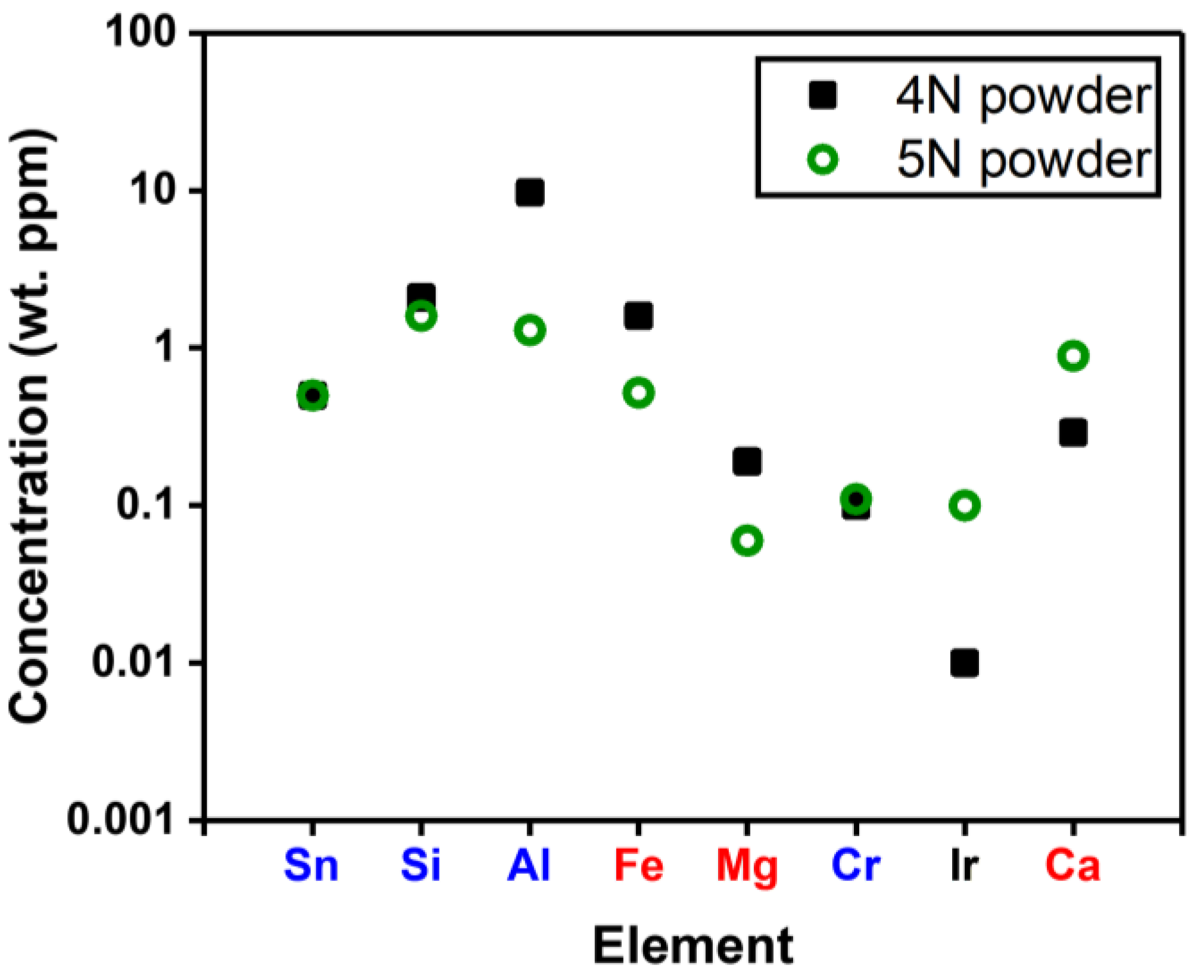
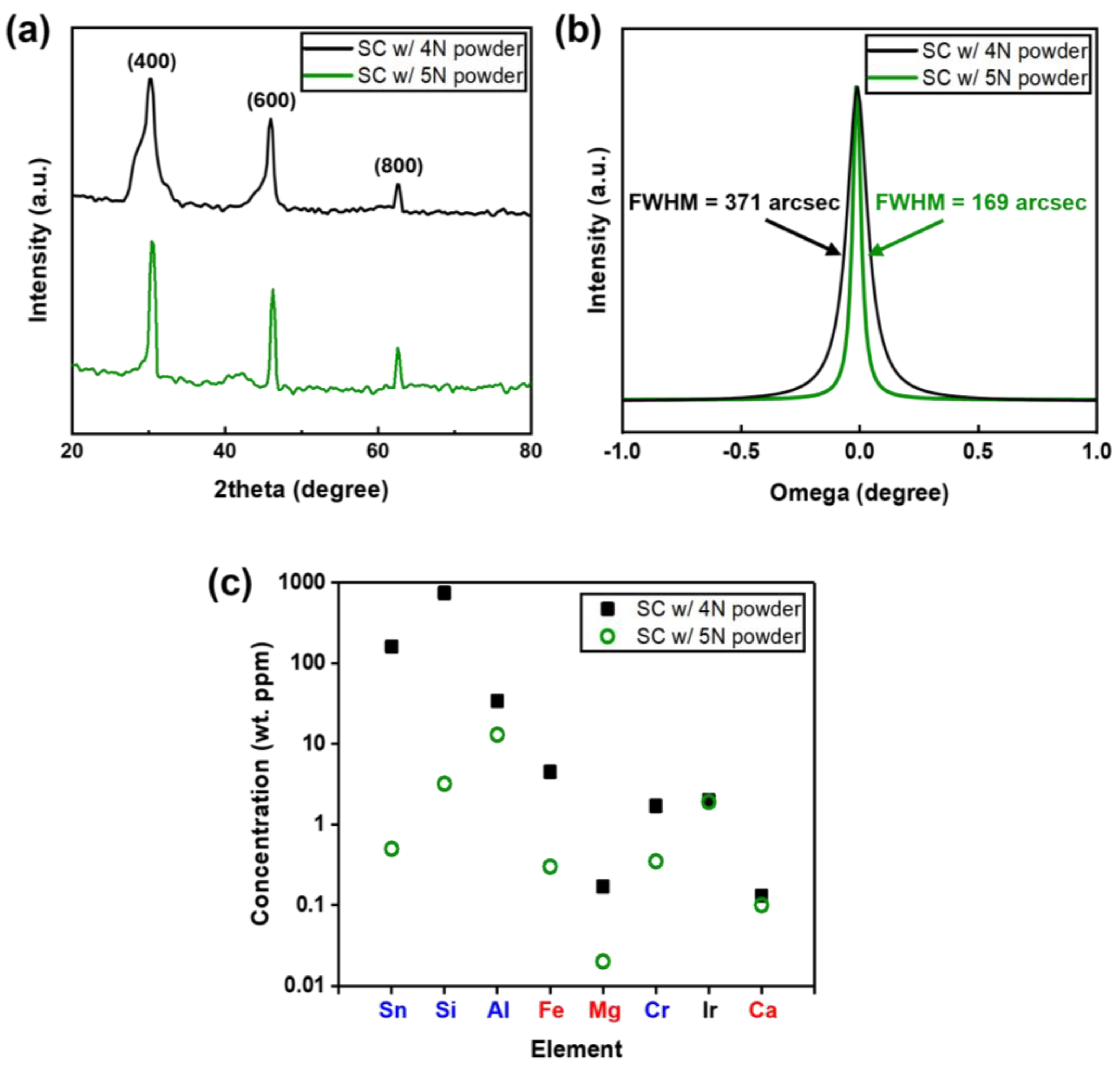
3.1. Effect of Powder Purity on β-Ga2O3 Crystal Growth
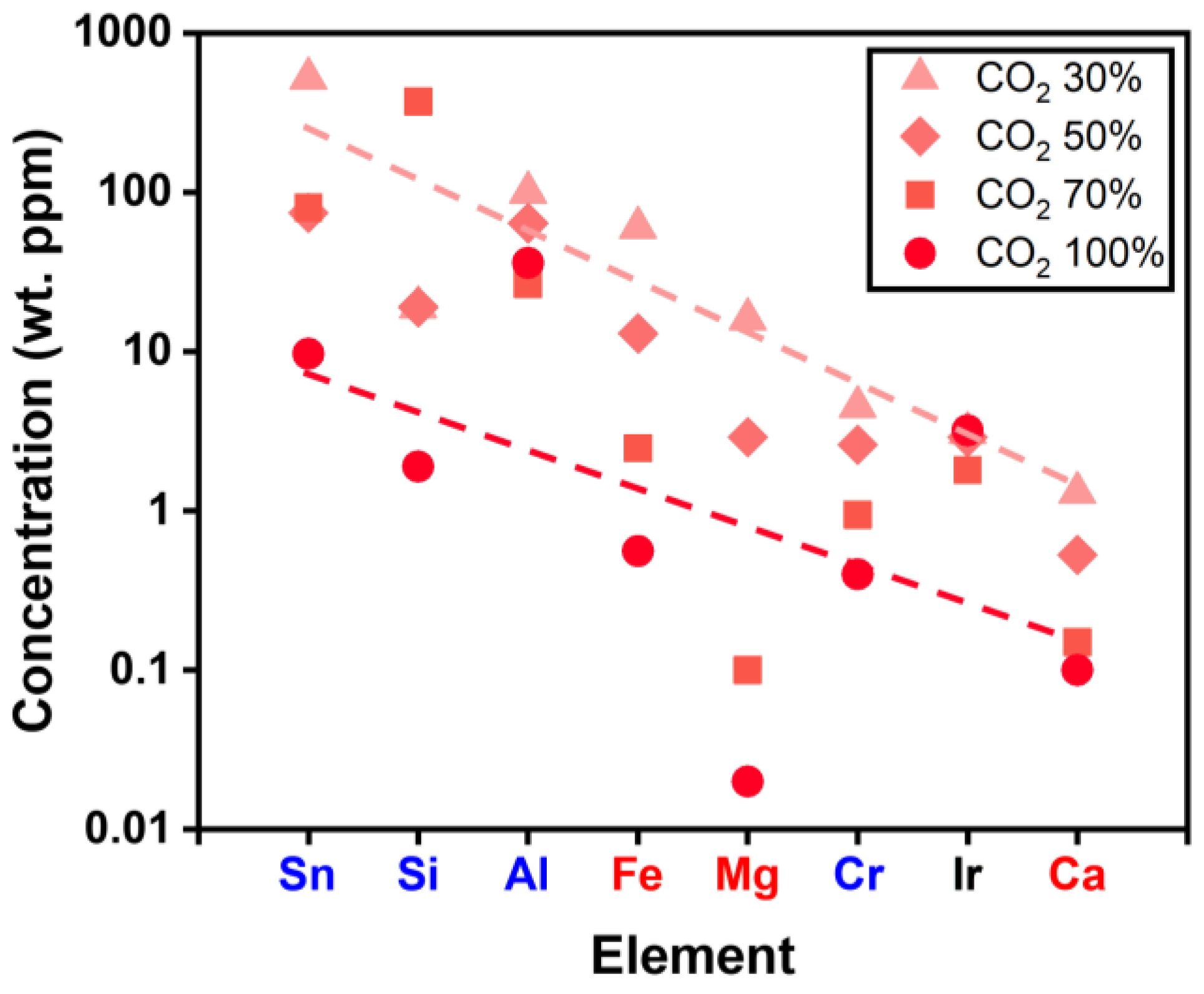
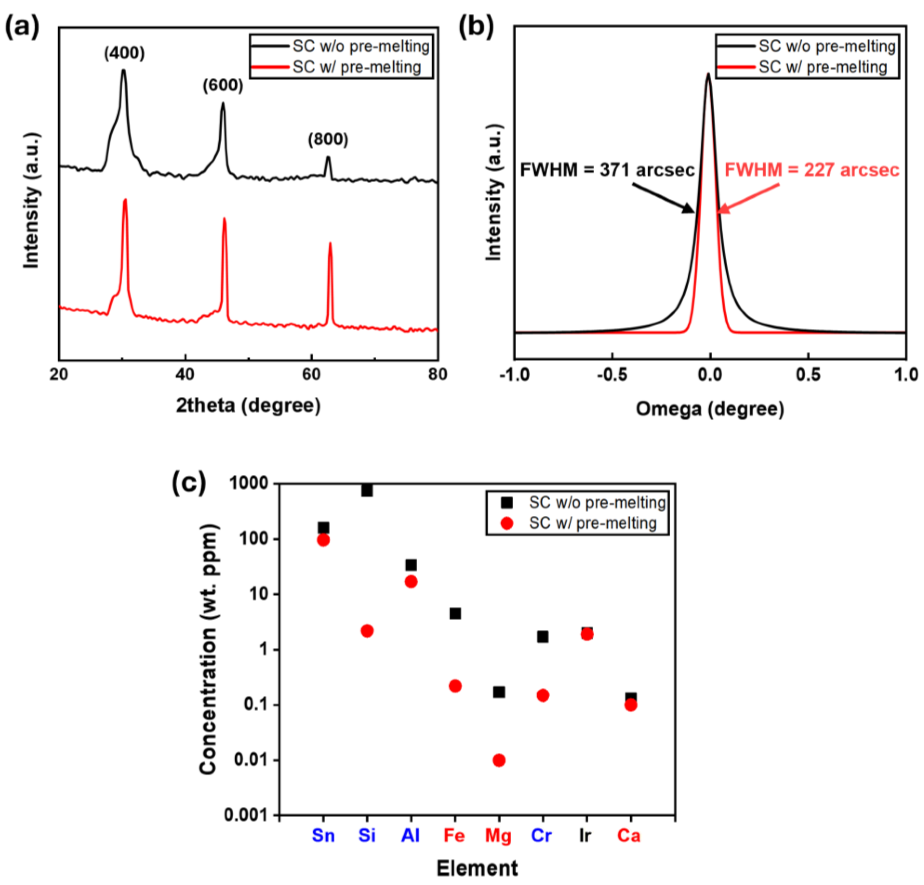
3.2. Effect of Pre-Melting Process on β-Ga2O3 Crystal Growth
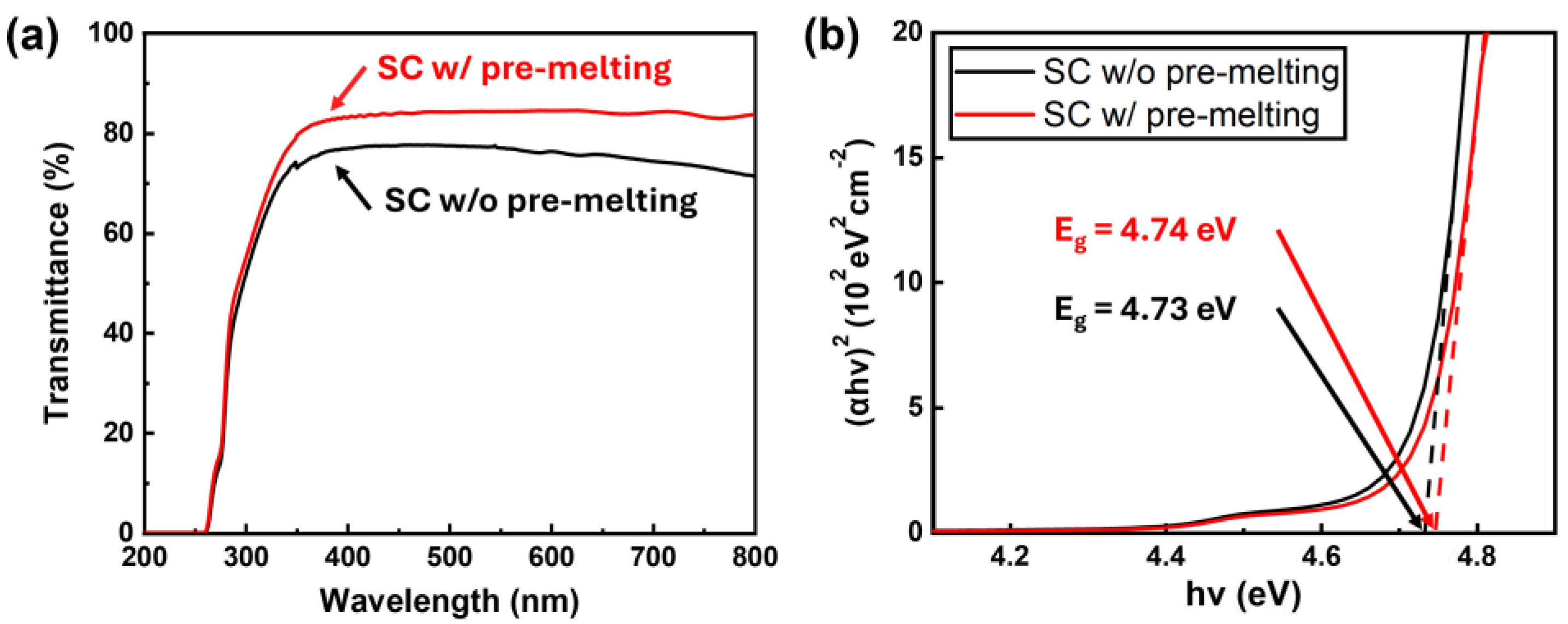
3.3. Optical and Electrical Properties
4. Conclusions
Author Contributions
Funding
Data Availability Statement
Conflicts of Interest
References
- Xue, H.; He, Q.; Jian, G.; Long, S.; Pang, T.; Liu, M. An Overview of the Ultrawide Bandgap Ga2O3 Semiconductor-Based Schottky Barrier Diode for Power Electronics Application. Nanoscale Res. Lett. 2018, 13, 290. [Google Scholar] [CrossRef]
- Pearton, S.J.; Ren, F.; Tadjer, M.; Kim, J. Perspective: Ga2O3 for Ultra-High Power Rectifiers and MOSFETS. J. Appl. Phys. 2018, 124, 220901. [Google Scholar] [CrossRef]
- Maimon, O.; Li, Q. Progress in Gallium Oxide Field-Effect Transistors for High-Power and RF Applications. Materials 2023, 16, 7693. [Google Scholar] [CrossRef]
- Chi, Z.; Asher, J.J.; Jennings, M.R.; Chikoidze, E.; Pérez-Tomás, A. Ga2O3 and Related Ultra-Wide Bandgap Power Semiconductor Oxides: New Energy Electronics Solutions for CO2 Emission Mitigation. Materials 2022, 15, 1164. [Google Scholar] [CrossRef] [PubMed]
- Tang, X.; Lu, Y.; Li, X. Flexible Gallium Oxide Electronics. Semicond. Sci. Technol. 2023, 38, 063001. [Google Scholar] [CrossRef]
- Kaneko, K.; Uno, K.; Jinno, R.; Fujita, S. Prospects for Phase Engineering of Semi-Stable Ga2O3 Semiconductor Thin Films Using Mist Chemical Vapor Deposition. J. Appl. Phys. 2022, 131, 090902. [Google Scholar] [CrossRef]
- Liu, Q.; Guo, D.; Chen, K.; Su, Y.; Wang, S.; Li, P.; Tang, W. Stabilizing the Metastable γ Phase in Ga2O3 Thin Films by Cu Doping. J. Alloys Compd. 2018, 731, 1225–1229. [Google Scholar] [CrossRef]
- Titov, A.I.; Karabeshkin, K.V.; Struchkov, A.I.; Nikolaev, V.I.; Azarov, A.; Gogova, D.S.; Karaseov, P.A. Comparative Study of Radiation Tolerance of GaN and Ga2O3 Polymorphs. Vacuum 2022, 200, 111005. [Google Scholar] [CrossRef]
- Ehrenreich, H. Band Structure and Electron Transport of GaAs. Phys. Rev. 1960, 120, 1951–1963. [Google Scholar] [CrossRef]
- Tairov, Y.M.; Tsvetkov, V.F. General Principles of Growing Large-Size Single Crystals of Various Silicon Carbide Polytypes. J. Cryst. Growth 1981, 52, 146–150. [Google Scholar] [CrossRef]
- Zhang, S.; Lian, X.; Ma, Y.; Liu, W.; Zhang, Y.; Xu, Y.; Cheng, H. Growth and Characterization of 2-Inch High Quality β-Ga2O3 Single Crystals Grown by EFG Method. J. Semicond. 2018, 39, 083003–083005. [Google Scholar] [CrossRef]
- Wei, J.; Bu, Y.; Sai, Q.; Qi, H.; Li, J.; Gu, H. Effect of High-Temperature Remelting on the Properties of Sn-Doped β-Ga2O3 Crystal Grown Using the EFG Method. CrystEngComm 2023, 25, 4317–4324. [Google Scholar] [CrossRef]
- Aida, H.; Nishiguchi, K.; Takeda, H.; Aota, N.; Sunakawa, K.; Yaguchi, Y. Growth of β-Ga2O3 Single Crystals by the Edge-Defined, Film Fed Growth Method. Jpn. J. Appl. Phys. 2008, 47, 8506. [Google Scholar] [CrossRef]
- Kim, H. Control and Understanding of Metal Contacts to β-Ga2O3 Single Crystals: A Review. SN Appl. Sci. 2022, 4, 27. [Google Scholar] [CrossRef]
- Ahmadi, E.; Oshima, Y. Materials Issues and Devices of α- and β-Ga2O3. J. Appl. Phys. 2019, 126, 160901. [Google Scholar] [CrossRef]
- Mu, W.; Jia, Z.; Yin, Y.; Hu, Q.; Li, Y.; Wu, B.; Zhang, J.; Tao, X. High Quality Crystal Growth and Anisotropic Physical Characterization of β-Ga2O3 Single Crystals Grown by EFG Method. J. Alloys Compd. 2017, 714, 453–458. [Google Scholar] [CrossRef]
- Fu, H.; Chen, H.; Huang, X.; Baranowski, I.; Montes, J.; Yang, T.-H.; Zhao, Y. Effect of Crystalline Anisotropy on Vertical (-201) and (010) Beta-Ga2O3 Schottky Barrier Diodes on EFG Single-Crystal Substrates. arXiv 2017, arXiv:1712.01318. [Google Scholar]
- Fu, B.; Jia, Z.; Mu, W.; Yin, Y.; Zhang, J.; Tao, X. A Review of β-Ga2O3 Single Crystal Defects, Their Effects on Device Performance and Their Formation Mechanism. J. Semicond. 2019, 40, 011804. [Google Scholar] [CrossRef]
- Fu, B.; Mu, W.; Zhang, J.; Wang, X.; Zhuang, W.; Yin, Y.; Jia, Z.; Tao, X. A Study on the Technical Improvement and the Crystalline Quality Optimization of Columnar β-Ga2O3 Crystal Growth by an EFG Method. CrystEngComm 2020, 22, 5060–5066. [Google Scholar] [CrossRef]
- Blevins, J.D.; Thomson, D.; Stevens, K.; Foundos, G. Growth of Single Crystal Beta-Gallium Oxide (β-Ga2O3) Semiconductor Material. CS MANTECH Proc. 2017, 22–25. [Google Scholar]
- Feng, G.; Li, S.; Tian, Y.; Qi, S.; Guo, D.; Tang, W. 2 in. Bulk β-Ga2O3 Single Crystals Grown by EFG Method with High Wafer-Scale Quality. ACS Omega 2024, 9, 22084–22089. [Google Scholar] [CrossRef] [PubMed]
- Tang, H.; He, N.; Zhang, H.; Liu, B.; Zhu, Z.; Xu, M.; Chen, L.; Liu, J.; Ouyang, X.; Xu, J. Inhibition of Volatilization and Polycrystalline Cracking, and the Optical Properties of β-Ga2O3 Grown by the EFG Method. CrystEngComm 2020, 22, 924–931. [Google Scholar] [CrossRef]
- Higashiwaki, M.; Fujita, S. Gallium Oxide: Materials Properties, Crystal Growth, and Devices; Springer Nature: Berlin/Heidelberg, Germany, 2020; ISBN 978-3-030-37153-1. [Google Scholar]
- Fu, B.; Jian, G.; Mu, W.; Li, Y.; Wang, H.; Jia, Z.; Li, Y.; Long, S.; Shi, Y.; Tao, X. Crystal Growth and Design of Sn-Doped β-Ga2O3: Morphology, Defect and Property Studies of Cylindrical Crystal by EFG. J. Alloys Compd. 2022, 896, 162830. [Google Scholar] [CrossRef]
- Kuramata, A.; Koshi, K.; Watanabe, S.; Yamaoka, Y.; Masui, T.; Yamakoshi, S. High-Quality β-Ga2O3 Single Crystals Grown by Edge-Defined Film-Fed Growth. Jpn. J. Appl. Phys. 2016, 55, 1202A2. [Google Scholar] [CrossRef]
- Wu, S.; Liu, Z.; Yang, H.; Wang, Y. Effects of Annealing on Surface Residual Impurities and Intrinsic Defects of β-Ga2O3. Crystals 2023, 13, 1045. [Google Scholar] [CrossRef]
- Haven, D.; Moutinho, H.; Mangum, J.S.; Guthrey, H.; Joyce, D.; Zakutayev, A.; Haegel, N.M. Multimodal Microscopy of Extended Defects in β-Ga2O3 (010) EFG Crystals. AIP Adv. 2023, 13, 075122. [Google Scholar] [CrossRef]
- Cui, H.; Sai, Q.; Qi, H.; Zhao, J.; Si, J.; Pan, M. Analysis on the Electronic Trap of β-Ga2O3 Single Crystal. J. Mater. Sci. 2019, 54, 12643–12649. [Google Scholar] [CrossRef]
- Heinemann, M.D.; Berry, J.; Teeter, G.; Unold, T.; Ginley, D. Oxygen Deficiency and Sn Doping of Amorphous Ga2O3. Appl. Phys. Lett. 2016, 108, 022107. [Google Scholar] [CrossRef]
- Higashiwaki, M. β-Ga2O3 Material Properties, Growth Technologies, and Devices: A Review. AAPPS Bull. 2022, 32, 3. [Google Scholar] [CrossRef]
- Dang, J.-N.; Zheng, S.; Chen, L.; Zheng, T. Electronic Structures and Optical Properties of Si- and Sn-Doped β-Ga2O3: A GGA+U Study*. Chin. Phys. B 2019, 28, 016301. [Google Scholar] [CrossRef]
- Neal, A.T.; Mou, S.; Rafique, S.; Zhao, H.; Ahmadi, E.; Speck, J.S.; Stevens, K.T.; Blevins, J.D.; Thomson, D.B.; Moser, N.; et al. Donors and Deep Acceptors in β-Ga2O3. Appl. Phys. Lett. 2018, 113, 062101. [Google Scholar] [CrossRef]
- Zeng, H.; Wu, M.; Gao, H.; Wang, Y.; Xu, H.; Cheng, M.; Lin, Q. Role of Native Defects in Fe-Doped β-Ga2O3. Materials 2023, 16, 6758. [Google Scholar] [CrossRef] [PubMed]
- Kim, H.W.; Myung, J.H. Ga2O3 Films Grown on Sapphire by the Thermal Evaporation of GaN Powders. Key Eng. Mater. 2007, 336–338, 637–639. [Google Scholar] [CrossRef]
- Chiang, J.-L.; Yadlapalli, B.K.; Chen, M.-I.; Wuu, D.-S. A Review on Gallium Oxide Materials from Solution Processes. Nanomaterials 2022, 12, 3601. [Google Scholar] [CrossRef] [PubMed]
- Varley, J.B.; Weber, J.R.; Janotti, A.; Van de Walle, C.G. Oxygen Vacancies and Donor Impurities in β-Ga2O3. Appl. Phys. Lett. 2010, 97, 142106. [Google Scholar] [CrossRef]
- Kim, S.; Ryou, H.; Gyu Lee, I.; Shin, M.; Jin Cho, B.; Sik Hwang, W. Impact of Al Doping on a Hydrothermally Synthesized β-Ga2O3 Nanostructure for Photocatalysis Applications. RSC Adv. 2021, 11, 7338–7346. [Google Scholar] [CrossRef]
- Huang, H.-L.; Chae, C.; Johnson, J.M.; Senckowski, A.; Sharma, S.; Singisetti, U.; Wong, M.H.; Hwang, J. Atomic Scale Defect Formation and Phase Transformation in Si Implanted β-Ga2O3. APL Mater. 2023, 11, 061113. [Google Scholar] [CrossRef]
- Shi, F.; Qiao, H. Photoluminescence Property of Cr-Doped β-Ga2O3 Nanorods Synthesized by a Hydrothermal Method. CrystEngComm 2020, 22, 7794–7799. [Google Scholar] [CrossRef]
- Peelaers, H.; Lyons, J.L.; Varley, J.; Van de Walle, C. Deep Acceptors and Their Diffusion in Ga2O3. APL Mater. 2019, 7, 022519. [Google Scholar] [CrossRef]
- McCluskey, M.D. Point Defects in Ga2O3. J. Appl. Phys. 2020, 127, 101101. [Google Scholar] [CrossRef]
- Zeng, H.; Ma, C.; Wu, M. Exploring the Effective P-Type Dopants in Two-Dimensional Ga2O3 by First-Principles Calculations. AIP Adv. 2024, 14, 055221. [Google Scholar] [CrossRef]
- Hachani, L.; Zaidat, K.; Saadi, B.; Wang, X.D.; Fautrelle, Y. Solidification of Sn–Pb Alloys: Experiments on the Influence of the Initial Concentration. Int. J. Therm. Sci. 2015, 91, 34–48. [Google Scholar] [CrossRef]
- Frodason, Y.K.; Krzyzaniak, P.P.; Vines, L.; Varley, J.B.; Van de Walle, C.G.; Johansen, K.M.H. Diffusion of Sn Donors in β-Ga2O3. APL Mater. 2023, 11, 041121. [Google Scholar] [CrossRef]
- Rahman, S.T.; Choi, J.-R.; Lee, J.-H.; Park, S.-J. The Role of CO2 as a Mild Oxidant in Oxidation and Dehydrogenation over Catalysts: A Review. Catalysts 2020, 10, 1075. [Google Scholar] [CrossRef]
- Kim, D.H.; Lim, D. Effects of Defects and Impurities on the Optical Properties and the Valley Polarization in Monolayer MoS2. J. Korean Phys. Soc. 2015, 66, 1564–1568. [Google Scholar] [CrossRef]
- Tauc, J.; Grigorovici, R.; Vancu, A. Optical Properties and Electronic Structure of Amorphous Germanium. Phys. Status Solidi B Basic. Solid. State Phys. 1966, 15, 627–637. [Google Scholar] [CrossRef]
- Li, S.; Yue, J.-Y.; Wu, C.; Liu, Z.; Yan, Z.-Y.; Li, P.-G.; Guo, D.-Y.; Wu, Z.-P.; Guo, Y.-F.; Tang, W.-H. Self-Powered Ultraviolet Photodetector Based on β-Ga2O3/WO3 NPs Heterojunction with Low Noise and High Visible Rejection. IEEE Sens. J. 2021, 21, 26724–26730. [Google Scholar] [CrossRef]
- Li, S.; Yan, Z.-Y.; Tang, J.-C.; Yue, J.-Y.; Liu, Z.; Li, P.-G.; Guo, Y.-F.; Tang, W.-H. Ga2O3/V2O5 Oxide Heterojunction Photovoltaic Photodetector with Superhigh Solar-Blind Spectral Discriminability. IEEE Trans. Electron. Devices 2022, 69, 2443–2448. [Google Scholar] [CrossRef]
- Li, S.; Yue, J.; Lu, C.; Yan, Z.; Liu, Z.; Li, P.; Guo, D.; Wu, Z.; Guo, Y.; Tang, W. Oxygen Vacancies Modulating Self-Powered Photoresponse in PEDOT:PSS/ε-Ga2O3 Heterojunction by Trapping Effect. Sci. China Technol. Sci. 2022, 65, 704–712. [Google Scholar] [CrossRef]
- Bennett, H.S.; Wilson, C.L. Statistical Comparisons of Data on Band-gap Narrowing in Heavily Doped Silicon: Electrical and Optical Measurements. J. Appl. Phys. 1984, 55, 3582–3587. [Google Scholar] [CrossRef]
- Wagner, J.; del Alamo, J.A. Band-gap Narrowing in Heavily Doped Silicon: A Comparison of Optical and Electrical Data. J. Appl. Phys. 1988, 63, 425–429. [Google Scholar] [CrossRef]
- Gulbransen, E.A.; Jansson, S.A. The High-Temperature Oxidation, Reduction, and Volatilization Reactions of Silicon and Silicon Carbide. Oxid. Met. 1972, 4, 181–201. [Google Scholar] [CrossRef]


| Property | Without Pre-Melting | With Pre-Melting | Remark |
|---|---|---|---|
| Carrier concentration (cm−3) | 8.1 × 10¹⁸ | 3.5 × 10¹⁸ | Hall |
| 1.7 × 10¹⁹ | 1.0 × 10¹⁸ | C−V | |
| Mobility (cm2/V·s) | 58 | 79.1 | Hall |
| Resistivity (Ω·cm) | 1.3 × 10⁻² | 2.3 × 10⁻² | Hall |
Disclaimer/Publisher’s Note: The statements, opinions and data contained in all publications are solely those of the individual author(s) and contributor(s) and not of MDPI and/or the editor(s). MDPI and/or the editor(s) disclaim responsibility for any injury to people or property resulting from any ideas, methods, instructions or products referred to in the content. |
© 2024 by the authors. Licensee MDPI, Basel, Switzerland. This article is an open access article distributed under the terms and conditions of the Creative Commons Attribution (CC BY) license (https://creativecommons.org/licenses/by/4.0/).
Share and Cite
Shin, A.-R.; Gu, T.-H.; Shin, Y.-J.; Jeong, S.-M.; Lee, H.; Bae, S.-Y. Pre-Melting-Assisted Impurity Control of β-Ga2O3 Single Crystals in Edge-Defined Film-Fed Growth. Nanomaterials 2025, 15, 7. https://doi.org/10.3390/nano15010007
Shin A-R, Gu T-H, Shin Y-J, Jeong S-M, Lee H, Bae S-Y. Pre-Melting-Assisted Impurity Control of β-Ga2O3 Single Crystals in Edge-Defined Film-Fed Growth. Nanomaterials. 2025; 15(1):7. https://doi.org/10.3390/nano15010007
Chicago/Turabian StyleShin, A-Ran, Tae-Hun Gu, Yun-Ji Shin, Seong-Min Jeong, Heesoo Lee, and Si-Young Bae. 2025. "Pre-Melting-Assisted Impurity Control of β-Ga2O3 Single Crystals in Edge-Defined Film-Fed Growth" Nanomaterials 15, no. 1: 7. https://doi.org/10.3390/nano15010007
APA StyleShin, A.-R., Gu, T.-H., Shin, Y.-J., Jeong, S.-M., Lee, H., & Bae, S.-Y. (2025). Pre-Melting-Assisted Impurity Control of β-Ga2O3 Single Crystals in Edge-Defined Film-Fed Growth. Nanomaterials, 15(1), 7. https://doi.org/10.3390/nano15010007