Article

Continuous-Wave Pumped Monolayer WS2 Lasing for Photonic Barcoding

1
Key Laboratory for Micro-Nano Physics and Technology of Hunan Province, College of Materials Science and Engineering, Hunan University, Changsha 410082, China
2
Hunan Institute of Optoelectronic Integration, Hunan University, Changsha 410082, China
3
Key Laboratory of Materials for High-Power Laser, Shanghai Institute of Optics and Fine Mechanics, Chinese Academy of Sciences, Shanghai 201800, China
4
Hangzhou Institute for Advanced Study, Chinese Academy of Sciences, Hangzhou 310024, China
*
Authors to whom correspondence should be addressed.
Nanomaterials 2024, 14(7), 614; https://doi.org/10.3390/nano14070614
Submission received: 2 March 2024 / Revised: 21 March 2024 / Accepted: 26 March 2024 / Published: 30 March 2024

Abstract

:
Micro/nano photonic barcoding has emerged as a promising technology for information security and anti-counterfeiting applications owing to its high security and robust tamper resistance. However, the practical application of conventional micro/nano photonic barcodes is constrained by limitations in encoding capacity and identification verification (e.g., broad emission bandwidth and the expense of pulsed lasers). Herein, we propose high-capacity photonic barcode labels by leveraging continuous-wave (CW) pumped monolayer tungsten disulfide (WS2) lasing. Large-area, high-quality monolayer WS2 films were grown via a vapor deposition method and coupled with external cavities to construct optically pumped microlasers, thus achieving an excellent CW-pumped lasing with a narrow linewidth (~0.39 nm) and a low threshold (~400 W cm−2) at room temperature. Each pixel within the photonic barcode labels consists of closely packed WS2 microlasers of varying sizes, demonstrating high-density and nonuniform multiple-mode lasing signals that facilitate barcode encoding. Notably, CW operation and narrow-linewidth lasing emission could significantly simplify detection. As proof of concept, a 20-pixel label exhibits a high encoding capacity (2.35 × 10108). This work may promote the advancement of two-dimensional materials micro/nanolasers and offer a promising platform for information encoding and security applications.

1. Introduction

Micro/nano photonic barcodes have prospered in the era of big data with significant values in information security and anti-counterfeiting. Their compact size, complicated structure, and unique optical properties allow them to be used for advanced identification and make them difficult to tamper with [1,2,3,4,5]. Micro/nano photonic barcodes are commonly classified as graphical and spectral barcodes. However, the graphic encoding labels lack security due to their predictable encoding methods, making them easy to copy [6]. Furthermore, the broad and overlapping spectral signals (typically the wavelength or relative intensity of fluorescence emission) diminish identification capabilities and compromise security levels [7]. Conversely, laser-based barcodes offer clear advantages with their narrow linewidth and brightness, making them reliable for identification. Researchers are exploring micro/nanolaser-based barcodes with different structures, like Whispering Gallery Mode (WGM) and Fabry–Perot [8,9,10,11,12,13]. However, these laser systems usually need expensive pulsed lasers for detection, obstructing their practicality. So, the key is developing room-temperature continuous-wave (CW) laser-based barcodes to overcome this limitation.
Recently, two-dimensional (2D) transition metal dichalcogenides (TMDCs) have attracted significant attention because of their potential to be used as micro/nanolasers owing to their atomic-scale thickness and high emission through small material volumes [14,15,16,17,18,19]. The spatial confinement effect at the atomic level leads to an extreme localization of the carriers, whereby photons are produced with carrier concentrations quickly reaching 1018 cm−3, fulfilling the population inversion requirement for the lasing process [14]. TMDC excitonic lasers have been fabricated by integrating a TMDC monolayer with an external cavity structure, such as a WSe2 monolayer with a GaP photonic crystal cavity [20], a WS2 with a SiO2/TiO2 distributed Bragg reflector vertical cavity [15] and MoTe2 with a Si nanobeam cavity [21]. Nevertheless, resonant cavities require complicated microfabrication processes, which could hinder the practical applications of 2D TMDC-based lasers. In addition, all previously mentioned TMDC-based lasers utilize a single or a few layers of TMDCs as the gain medium produced by mechanical exfoliation, a pathway whose low controllability and repeatability further limit the application of micro/nanolasers.
In this paper, we report a novel high-capacity photonic barcode label by leveraging CW-pumped monolayer WS2 lasing. Specifically, large-area, high-quality monolayer WS2 films prepared via vapor deposition serve as gain mediums for external WGM resonant cavities and facilitate the construction of optically pumped microlasers. With the lensing and shielding effects of the resonant cavity, an excellent CW-pumped lasing with a full-width-half-maximum (FWHM) as low as 0.39 nm and an excitation threshold of 400 W cm−2 was achieved at room temperature. Furthermore, we systematically investigate the influence of resonant cavity sizes and the WS2 WGM lasing properties. Using a confocal microfluorescence system, we acquired high-density and nonuniform multiple-mode lasing signals suitable for barcode encoding through the lasing mapping of a photonic barcode label composed of closely packed WS2 microlasers with different sizes. Moreover, CW operation and narrow-linewidth lasing emission could greatly simplify detection. Remarkably, even with only 20 pixels captured, the 20-pixel label demonstrated an impressive encoding capacity of 2.35 × 10108. This work may promote the advancement of 2D material-based micro/nanolasers and offer a promising platform for information encoding and security applications.

2. Methods

2.1. Synthesis of Monolayer WS2 Films

Monolayer WS2 single-crystal films were grown in a tube furnace with domain-confined chemical vapor deposition (CVD) (Figure 1a). Two pieces of cleaned 300 nm SiO2/Si substrates formed a sandwich structure face-to-face with the mental tungsten precursor (WO3 powder, 3 mg) at the center and were placed together in a porcelain boat. High-purity sulfur powder (800 mg) was used as the S source. The S and the substrate zone temperatures were ~200 °C and ~770 °C, respectively. High-purity N2 was used as the carrier gas at a 65 mL/min flow rate, resulting in slow S precursor diffusion during the synthesis. This growth process was performed within 10 min at the grown temperature, and the furnace was left to cool naturally to room temperature.

2.2. Preparation of the WS2 Microlaser

As-grown WS2 films were used to fabricate WS2 microlasers coupled with external optical cavities. The resonant cavities with different sizes (5, 7, 10, 15 µm) were dispersed in anhydrous ethanol at a 3% volume fraction and sonicated for 10 min to ensure a uniform dispersion. Subsequently, the cavities were spin-coated onto as-grown WS2 films at a speed of 3000 rpm for 30 s and dried naturally.

2.3. Readout and Digitization of Photonic Barcode Labels

A confocal photoluminescence (PL) system was used to read photonic barcodes, and a 405 nm laser was used as the excitation source. PL mapping data were obtained for different pixels (1, 5, and 20) by moving the carrier stage. The rule for photonic barcode label identification was defined as follows: (1) setting 0.25 times the normalized PL intensity as the threshold intensity; values above and below the threshold were set to “1” and “0”, respectively; (2) the width of each bit was specified to be 2.5 nm. Finally, the emission spectra of the WS2 microlaser were converted to photonic barcode labels using “1” (white) and “0” (black) as symbols.

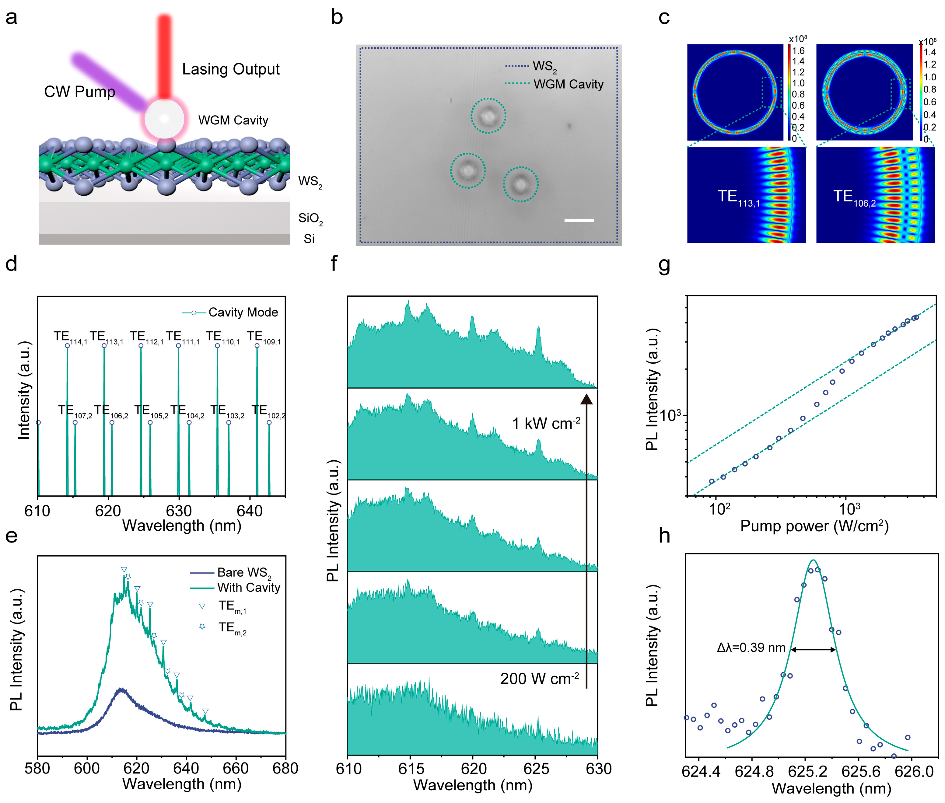
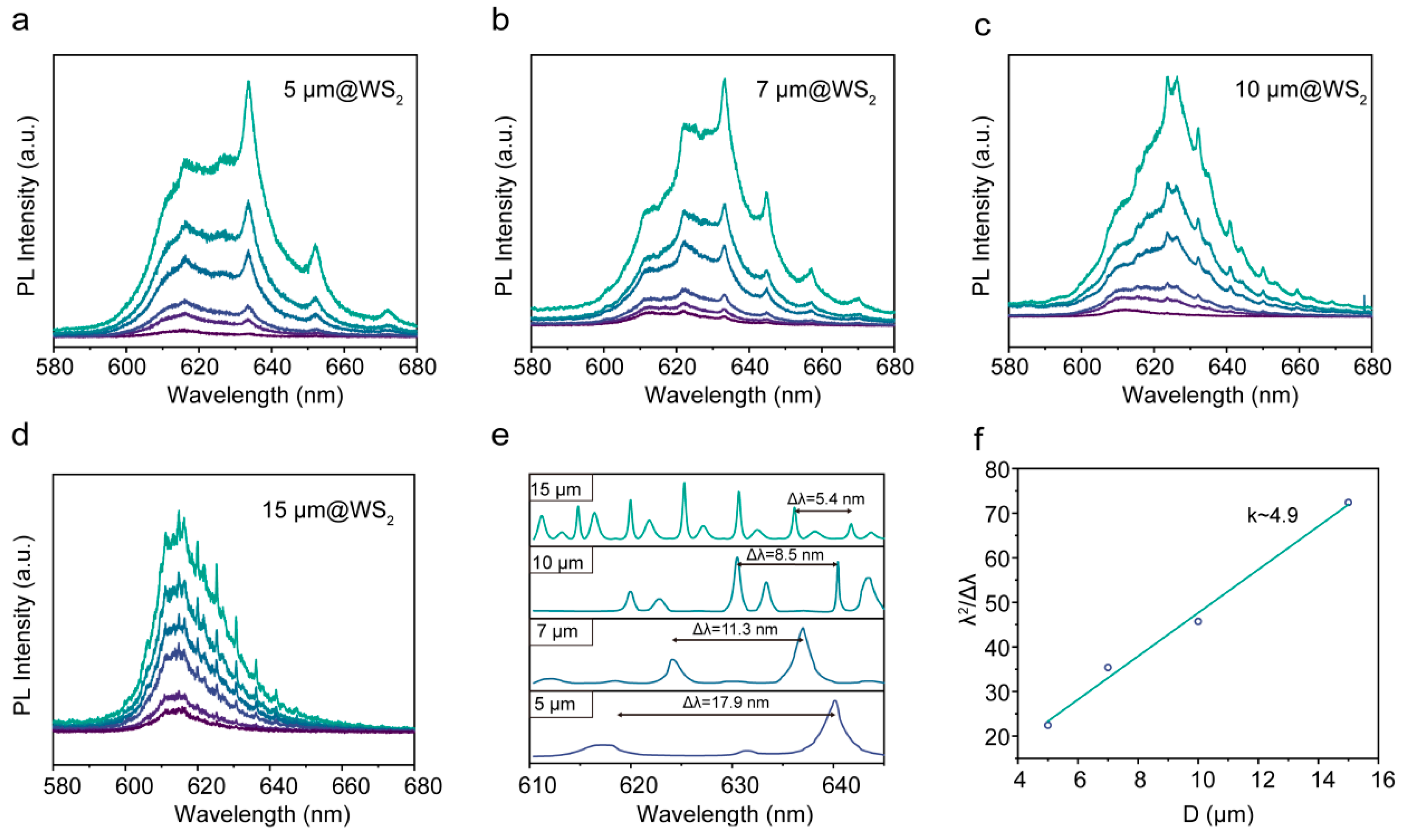
3. Results and Discussion

In contrast to the previously reported growth techniques for WS2 thin films, we successfully synthesized hundred-micron single-crystal monolayer WS2 in one step at 770 °C (Figure 1a), as opposed to employing a two-step process or a higher-temperature system [22,23]. The photograph and optical image of the as-grown WS2 sample show that our method achieved large-area WS2 films on silica substrates, and color contrast directly shows large, thin WS2 films in the central region and small, thick samples at the edges (Figure 1b,c). The as-grown monolayer WS2 has a regular triangular shape with a maximum edge length of 170 µm. Scanning electron microscopy images reveal that the WS2 films have flat, clean atomic surfaces and sharp edges, as shown in Figure 1d. We measured the thicknesses of these triangular films using the height profile obtained from atomic force microscopy (AFM) and Raman spectroscopy. The AFM image (Figure S1) indicates that the as-grown WS2 films are monolayers, consistent with the monolayer WS2 thickness reported in the existing literature [24]. The crystal structure of WS2 films was confirmed by transmission electron microscopy (TEM) in Figure 1e. The as-grown WS2 sample was transferred onto Cu grids and then characterized. The high-resolution TEM image demonstrates a hexagonal ring lattice of alternating tungsten atoms (dark dots) and sulfur atoms (gray dots). The interplanar distance of (1 0 0) was calculated to be 0.27 nm, which conforms with the 2H-WS2 crystal structure. Moreover, selected area electron diffraction (SAED) analysis confirmed the synthesis of monolayer single-crystal WS2 with semiconductor properties (Figure S2). Energy dispersive X-ray spectroscopy (EDS) and X-ray photoelectron spectroscopy (XPS) were performed to identify the composition of the as-grown WS2 films. The EDS elemental mappings, as depicted in Figure 1e, reveal that W and S elements are evenly distributed in the single-crystal films. Figure 1f–h present the XPS images of the as-grown WS2 films. The full spectra show that high-quality WS2 films were synthesized without impurities (Figure 1f). The fine spectra analysis of S and W led to the conclusion that the precursors were wholly transformed into WS2 rather than intermediate products such as WS2xO2−2x [24]. All data unambiguously show that triangular monolayer WS2 films were synthesized with large-scale uniformity and high single-crystal by the CVD method. The large dimensions, perfect triangular shape, and clean surface of the monolayer WS2 make it an ideal candidate for gaining fundamental knowledge and developing practical applications for 2D semiconductors.
Micro-area reflectance and photoluminescence (PL) spectroscopy were employed to investigate the light emission from the as-grown WS2, as illustrated in Figure 2a. A prominent absorption peak at 613 nm in the reflectance curve aligns well with the PL peak of the monolayer WS2. Further analysis of the PL curve reveals a distinct emission peak at 613.6 nm (~2.02 eV), attributed to the neutral exciton (X0) according to previous studies (Figure 2b) [25,26,27,28]. In addition, a weaker luminescence peak at 624.2 nm (~1.98 eV) was identified as the charged exciton or Trion (XT). These favorable luminescence characteristics proved the high quality of the synthesized WS2 monolayer. The inset of Figure 2b presents a PL intensity mapping image of a uniform triangular WS2 monolayer across the sample region. The darkest area at the center may be attributed to local environmental changes, sample defects, and growth-induced strain [24]. Raman spectroscopy has been widely employed to explore molecular vibrations and rotations in 2D materials, especially for analyzing the number of layers [29,30,31], molecular doping effects [32], and internal and external strains [33]. Figure 2c,d show the Raman spectra of the as-grown WS2 monolayer over a frequency range from 130 cm−1 to 500 cm−1 with laser excitation at 532 nm. Typical Raman modes of WS2 are present, as labeled. There are first-order Raman modes, including LA (M), LA (K), E12g (Γ), E12g (M), and A1g (Γ), and second-order modes, such as 2LA (M). The frequency difference between E12g (in-plane mode of S and W atoms) and A1g (out-of-plane mode of S atoms) was 62.6 cm−1, confirming that the as-grown WS2 films were monolayer. The Raman intensity image of A1g mode (inset of Figure 2c) also clearly shows the perfect triangular shape and uniform thickness of the WS2 films. The as-grown monolayer WS2, with excellent luminescent performance and uniformity, offers a fantastic material choice for micro/nano light-emitting devices.
The lasing characteristics of the WS2 microlaser were studied via a homebuilt micro-PL system after introducing external cavities onto the as-grown WS2 films to construct the microlaser, whereby a 405 nm CW laser was focused down to 5 µm and functioned as the pump source. Figure 3a shows a schematic image of the WS2 microlaser. The high-quality optical resonant cavity can prominently enhance the light–matter interaction of the WS2 gain medium, thereby improving the resonant emission of the WS2 microlaser. Figure 3b shows the perfect circular boundaries and the ultrasmooth surfaces of the external cavities in the WS2 microlaser. Dispersed resonant cavities were distributed on top of the as-grown WS2 films on a 300 nm SiO2/Si substrate, which was selected to enhance the absorption and emission efficiency because of constructive interference and a reduction in the lattice distortion [34,35]. To identify the resonance of the laser structure, Figure 3c,d illustrate the simulated electric field distribution of the WS2 microlaser cavity as executed by the finite element method. The analysis only considered the transverse electric (TE). According to the mode simulations, strong and weak modes are associated with fundamental modes (TEm,1) and higher-order modes (TEm,2). Figure 3c presents the electric field profile for different mode numbers. The calculated mode positions distinguished the oscillatory peaks into two groups, as shown in Figure 3d. Experimentally, a series of sharp peaks were superimposed onto the broad emission spectra, which indicates that the external resonant cavity formed typical WGM resonant feedback (Figure 3e). Moreover, the emission intensity of the WS2 microlaser was approximately four times higher than that of the grown substrate, as intuitively seen in the PL intensity mapping image shown in Figure S3. This phenomenon can be attributed to the lensing effect, in which excitation energy is localized at the resonant cavity and WS2 interface, which can significantly improve the excitation efficiency and expand spatial overlap between the excitation and gain regions [36]. Additionally, the center wavelength of the WS2 microlaser exhibited a red shift of ~13 meV compared with the surrounding bare monolayer WS2. This red shift may be attributed to screening and strain effects caused by the resonant cavity [37,38,39]. For both the WS2 microlaser and the bare WS2, the frequency separation between typical Raman feature modes of E12g and A1g was 62.5 cm−1 (Figure S4), indicating that the strain effect can be ignored [40,41].
We investigated the non-linear emission characteristics of the WS2 microlaser by acquiring its PL spectra at various power densities ranging from 93 to 2300 W cm−2, as depicted in Figure 3f. At low excitation power, the PL spectrum of the microlaser closely resembled that of bare WS2, dominated by spontaneous emission (SE) with a broader bandwidth. As the excitation power gradually increased, a progressive narrowing of the prominent emission peaks was observed. Figure 3g presents the power dependence curve for the emission peak intensity at 625.2 nm. The curve exhibits an inflection point, signifying a transition from linear to superlinear photon density increase. This inflection corresponds to a lasing threshold of approximately 400 W cm−2. Below the threshold, the curve exhibits linear behavior consistent with SE. Beyond the threshold, the non-linear increase indicates amplified spontaneous emission and subsequent lasing, resulting in the characteristic S-shape. In comparison, the emission intensity of bare WS2 exhibits only linear SE behavior across the entire pumping range (Figure S5), further substantiating the role of the resonant cavity in enabling lasing in the microlaser. The extracted photon intensity of the lasing emission was fitted using a Lorentzian function, revealing a narrow linewidth of 0.39 nm (Figure 3h). This narrow linewidth, corresponding to a quality factor of 1560, further corroborates the occurrence of lasing action in the WS2 microlaser.
To systematically explore the influence of resonant cavity size on WS2 lasing properties, the microlasers were fabricated with purposefully varied cavity dimensions, as illustrated in Figure 4a–d. Each spectrum exhibits distinct multi-mode lasing peaks, with the number of peaks increasing as the cavity size grows. Figure 4e presents the background-subtracted emission spectra of WS2 microlasers with different sizes. Notably, the spacing between adjacent fundamental modes exhibits a systematic decrease, from 17.9 nm to 11.3 nm, 8.5 nm, and 5.4 nm, respectively, as the cavity size increases from 5 µm to 7 µm, 10 µm, and 15 µm. As is well known, the WGM modulation peaks follow the equation:
Δλ = λ2/π D ηeff
where Δλ is the free spectral range (FSR) of the spacing between two adjacent same-order resonant modes. λ is the resonant wavelength. D is the diameter of the resonant cavity, and ηeff is the group effective index of refraction [42]. When the optical path consists of an integer multiple of the emission wavelength, the resonance emission is strengthened for the light overlap. Therefore, the resonant wavelength (λ) depends on the cavity size (D) and refractive index (η), as evident in Figure 4e. The observed variation in resonant emission wavelengths across different microlaser sizes aligns with this principle. The FSR is an α/D (where α is a constant) function of the diameters of the resonant cavities, which supports that the resonant modes can be attributed to WGM modulation [43]. Figure 4f shows the relationship between λ2/Δλ and D. The simulation result obtained by linear fitting reveals that the slope ηπ is 5.0, which agrees with the observed slope of 4.9. Here, η is determined to be 1.59, as π is set to 3.14.
Inspired by the unique spectral signals associated with cavity sizes, we propose a photonic barcode concept derived from the WS2 microlaser, schematically illustrated in Figure 5a. Owing to the distinct sizes of individual resonant cavities, the sharp lasing signals could serve as a fingerprint for each pixel, enabling their differentiation based on their characteristic emission spectra. By using a confocal microfluorescence system, we acquired high-density and nonuniform multiple-mode lasing signals, as shown in Figure 5b. Based on the spectral variations between different cavities, we encoded the lasing peaks of the WS2 microlaser to generate a series of corresponding photonic barcode labels.
A typical barcode label comprises a series of black bars and blanks of varying widths to represent a set of information graphically. Herein, photonic barcode labels are defined as follows: after normalizing the intensity of the WS2 microlaser lasing peaks, an intensity of 0.25 is specified as the intensity threshold, as shown by the horizontal dotted line in Figure 5c. All emission peaks with intensity above the threshold intensity were set to “1”, as indicated by the black bars; conversely, those below the threshold intensity were defined as “0”, as noted in the blank bars. The width of each bit was set to 2.5 nm. We intercepted each emission spectra from 610 nm to 655 nm, meaning a single pixel has 18 bits of “1”/“0”. According to the coding rule, we can deduce a specific photonic barcode label (Figure 5c) from the modulated spectra. In other words, a one-to-one correspondence between each photonic barcode label and the WS2 microlaser spectra exists, directly related to the dimensions of the resonant cavity. As proof of concept, we explored their application potential for anticounterfeit labels. We examined the optical performance of 5 and 20 pixels by line-by-line scanning and measuring the lasing emission of these microlasers. Figure 5d,e illustrate the acquired lasing spectra and corresponding photonic barcode labels. Surprisingly, the 20-pixel label demonstrated an impressive encoding capacity of 2.35 × 10108, even with only 20 pixels captured, virtually eliminating the possibility of duplication. These results suggest that photonic barcode labels utilizing CW-pumped WS2 microlasers could offer high sampling efficiency and enhanced security for authentication purposes, making them a promising application for anti-counterfeiting.

4. Conclusions

In summary, we proposed an original high-capacity photonic barcode label that utilized the CW-pumped WS2 lasing. The WS2 microlaser, based on large-area monolayer WS2 films, demonstrated superior lasing characteristics at room temperature, including a narrow linewidth (~0.39 nm) and a low threshold (~400 W cm−2) under CW pumping. Moreover, we successfully fabricated photonic barcode labels composed of a closely packed WS2 microlaser of varying sizes. These labels exhibit high-density and nonuniform multiple-mode lasing signals facilitating barcode encoding. As proof of concept, a 20-pixel label demonstrated a high encoding capacity (2.35 × 10108), indicating its potential as a platform for information encoding and security applications.

Supplementary Materials

The following supporting information can be downloaded at: https://www.mdpi.com/article/10.3390/nano14070614/s1, Figure S1. (a) AFM image of a monolayer CVD-grown WS2. (b) The height profile curve along the solid green line in (a). The thickness of as-grown monolayer WS2 is about 0.78 nm; Figure S2. (a) A low-magnification TEM image of the triangular WS2 monolayer transferred onto Cu grids. (b) SAED pattern of the WS2 at the location of the green box in (a). Inset: calibration of the SAED pattern; Figure S3. PL mapping image of CVD-grown WS2 with the external cavities by plotting intensity at 620 nm when the pumping power was 500 W cm−2. Scale bar is 10 μm; Figure S4. Raman spectra of monolayer WS2 and WS2 coupled with the resonant cavity. The difference in wavenumber between E2g and A1g characteristic modes is 62.5 cm−1, which confirms that the CVD-grown WS2 films are monolayer. The vigorous intensity of Si at 520 cm−1 is another evidence of synthesized ultra-thin WS2; Figure S5. PL spectra of bare WS2 at different excitation powers. The excitation power is 100 W cm−2, 200 W cm−2, 300 W cm−2, 400 W cm−2, 600 W cm−2, 700 W cm−2, and 1 kW cm−2 in order from low to high.

Author Contributions

Conceptualization, H.C., W.M. and H.D.; methodology and validation, H.C. and W.M.; data analysis and visualization, W.M. and J.Q.; original draft writing, H.C.; review and editing, W.M. and J.Q.; supervision, H.D. and S.C. All authors have read and agreed to the published version of the manuscript.

Funding

This research was funded by the National Natural Science Foundation of China (Nos. 61925506, 12374297, 62305078), Hangzhou Science and Technology Bureau of Zhejiang Province (No. TD2020002). H.D. acknowledges the Academic/Technology Research Leader Program of Shanghai (23XD1404500).

Data Availability Statement

All the relevant data that support the findings of this study are available from the corresponding authors on reasonable request.

Conflicts of Interest

The authors declare no conflicts of interest.

References

  1. Anwar, A.R.; Mur, M.; Humar, M. Microcavity- and Microlaser-Based Optical Barcoding: A Review of Encoding Techniques and Applications. ACS Photonics 2023, 10, 1202–1224. [Google Scholar] [CrossRef]
  2. Hou, Y.; Gao, Z.; Zhao, Y.S.; Yan, Y. Organic Micro/Nanoscale Materials for Photonic Barcodes. Org. Chem. Front. 2020, 7, 2776–2788. [Google Scholar] [CrossRef]
  3. Deneff, J.I.; Butler, K.S.; Rohwer, L.E.S.; Pearce, C.J.; Valdez, N.R.; Rodriguez, M.A.; Luk, T.S.; Sava Gallis, D.F. Encoding Multilayer Complexity in Anti-Counterfeiting Heterometallic MOF-Based Optical Tags. Angew. Chem. Int. Ed. 2021, 60, 1203–1211. [Google Scholar] [CrossRef] [PubMed]
  4. Liu, Y.; Shang, L.; Wang, H.; Zhang, H.; Zou, M.; Zhao, Y. Multicolored Photonic Barcodes from Dynamic Micromolding. Mater. Horiz. 2018, 5, 979–983. [Google Scholar] [CrossRef]
  5. Yao, W.; Tian, Q.; Wu, W. Tunable Emissions of Upconversion Fluorescence for Security Applications. Adv. Opt. Mater. 2019, 7, 1801171. [Google Scholar] [CrossRef]
  6. Lee, S.; Pekdemir, S.; Kayaci, N.; Kalay, M.; Onses, M.S.; Ye, J. Graphene-Based Physically Unclonable Functions with Dual Source of Randomness. ACS Appl. Mater. Interfaces 2023, 15, 33878–33889. [Google Scholar] [CrossRef]
  7. Lee, H.; Kim, J.; Kim, H.; Kim, J.; Kwon, S. Colour-Barcoded Magnetic Microparticles for Multiplexed Bioassays. Nat. Mater. 2010, 9, 745–749. [Google Scholar] [CrossRef]
  8. Huang, C.; Lucas, B.; Vervaet, C.; Braeckmans, K.; Van Calenbergh, S.; Karalic, I.; Vandewoestyne, M.; Deforce, D.; Demeester, J.; De Smedt, S.C. Unbreakable Codes in Electrospun Fibers: Digitally Encoded Polymers to Stop Medicine Counterfeiting. Adv. Mater. 2010, 22, 2657–2662. [Google Scholar] [CrossRef]
  9. Fan, Y.; Zhang, C.; Gao, Z.; Zhou, W.; Hou, Y.; Zhou, Z.; Yao, J.; Zhao, Y.S. Randomly Induced Phase Transformation in Silk Protein-Based Microlaser Arrays for Anticounterfeiting. Adv. Mater. 2021, 33, 2102586. [Google Scholar] [CrossRef]
  10. Zhang, L.; Li, H.; Yang, Y.; Cui, Y.; Qian, G. Tunable NIR Lasing in MOF for Multi-Level Complex Photonic Barcodes. Adv. Opt. Mater. 2023, 11, 2202714. [Google Scholar] [CrossRef]
  11. Mao, W.; Gao, X.; Li, B.; Zhang, Y.; Wang, P.; Dong, H.; Zhang, L. Randomized Whispering-Gallery-Mode Microdisk Laser Arrays via Cavity Deformations for Anti-Counterfeiting Labels. Photonics Res. 2023, 11, 1227. [Google Scholar] [CrossRef]
  12. Gao, X.; Wang, H.; Dong, H.; Shao, J.; Shao, Y.; Zhang, L. Tunable Key-Size Physical Unclonable Functions Based on Phase Segregation in Mixed Halide Perovskites. ACS Appl. Mater. Interfaces 2023, 15, 23429–23438. [Google Scholar] [CrossRef]
  13. Mao, W.; Li, H.; Tang, B.; Zhang, C.; Liu, L.; Wang, P.; Dong, H.; Zhang, L. Laser Patterning of Large-Scale Perovskite Single-Crystal-Based Arrays for Single-Mode Laser Displays. Int. J. Extrem. Manuf. 2023, 5, 045001. [Google Scholar] [CrossRef]
  14. Salehzadeh, O.; Djavid, M.; Tran, N.H.; Shih, I.; Mi, Z. Optically Pumped Two-Dimensional MoS2 Lasers Operating at Room-Temperature. Nano Lett. 2015, 15, 5302–5306. [Google Scholar] [CrossRef] [PubMed]
  15. Shang, J.; Cong, C.; Wang, Z.; Peimyoo, N.; Wu, L.; Zou, C.; Chen, Y.; Chin, X.Y.; Wang, J.; Soci, C.; et al. Room-Temperature 2D Semiconductor Activated Vertical-Cavity Surface-Emitting Lasers. Nat. Commun. 2017, 8, 543. [Google Scholar] [CrossRef]
  16. Tran, T.T.; Wang, D.; Xu, Z.-Q.; Yang, A.; Toth, M.; Odom, T.W.; Aharonovich, I. Deterministic Coupling of Quantum Emitters in 2D Materials to Plasmonic Nanocavity Arrays. Nano Lett. 2017, 17, 2634–2639. [Google Scholar] [CrossRef]
  17. Zhang, Y.; Wang, S.; Chen, S.; Zhang, Q.; Wang, X.; Zhu, X.; Zhang, X.; Xu, X.; Yang, T.; He, M.; et al. Wavelength-Tunable Mid-Infrared Lasing from Black Phosphorus Nanosheets. Adv. Mater. 2020, 32, 1808319. [Google Scholar] [CrossRef] [PubMed]
  18. Fang, H.; Liu, J.; Lin, Q.; Su, R.; Wei, Y.; Krauss, T.F.; Li, J.; Wang, Y.; Wang, X. Laser-Like Emission from a Sandwiched MoTe2 Heterostructure on a Silicon Single-Mode Resonator. Adv. Opt. Mater. 2019, 7, 1900538. [Google Scholar] [CrossRef]
  19. Liang, C.; Wang, E.; Li, X.; Wang, J.; Liu, Y.; Chen, B.; Chen, H.; Liu, Y.; Peng, X. Optical Limiting Performances of Transitional Metal Dichalcogenides MX2 (M = V, Nb, Ta; X = S, Se) with Ultralow Initial Threshold and Optical Limiting Threshold. Chin. Opt. Lett. 2022, 20, 021901. [Google Scholar] [CrossRef]
  20. Wu, S.; Buckley, S.; Schaibley, J.R.; Feng, L.; Yan, J.; Mandrus, D.G.; Hatami, F.; Yao, W.; Vučković, J.; Majumdar, A.; et al. Monolayer Semiconductor Nanocavity Lasers with Ultralow Thresholds. Nature 2015, 520, 69–72. [Google Scholar] [CrossRef]
  21. Li, Y.; Zhang, J.; Huang, D.; Sun, H.; Fan, F.; Feng, J.; Wang, Z.; Ning, C.Z. Room-Temperature Continuous-Wave Lasing from Monolayer Molybdenum Ditelluride Integrated with a Silicon Nanobeam Cavity. Nat. Nanotechnol. 2017, 12, 987–992. [Google Scholar] [CrossRef] [PubMed]
  22. Gutiérrez, H.R.; Perea-López, N.; Elías, A.L.; Berkdemir, A.; Wang, B.; Lv, R.; López-Urías, F.; Crespi, V.H.; Terrones, H.; Terrones, M. Extraordinary Room-Temperature Photoluminescence in Triangular WS2 Monolayers. Nano Lett. 2013, 13, 3447–3454. [Google Scholar] [CrossRef] [PubMed]
  23. Lan, F.; Yang, R.; Xu, Y.; Qian, S.; Zhang, S.; Cheng, H.; Zhang, Y. Synthesis of Large-Scale Single-Crystalline Monolayer WS2 Using a Semi-Sealed Method. Nanomaterials 2018, 8, 100. [Google Scholar] [CrossRef] [PubMed]
  24. Cong, C.; Shang, J.; Wu, X.; Cao, B.; Peimyoo, N.; Qiu, C.; Sun, L.; Yu, T. Synthesis and Optical Properties of Large-Area Single-Crystalline 2D Semiconductor WS2 Monolayer from Chemical Vapor Deposition. Adv. Opt. Mater. 2014, 2, 131–136. [Google Scholar] [CrossRef]
  25. Shi, J.; Zhu, J.; Wu, X.; Zheng, B.; Chen, J.; Sui, X.; Zhang, S.; Shi, J.; Du, W.; Zhong, Y.; et al. Enhanced Trion Emission and Carrier Dynamics in Monolayer WS2 Coupled with Plasmonic Nanocavity. Adv. Opt. Mater. 2020, 8, 2001147. [Google Scholar] [CrossRef]
  26. Kwon, Y.; Kim, K.; Kim, W.; Ryu, S.; Cheong, H. Variation of Photoluminescence Spectral Line Shape of Monolayer WS2. Curr. Appl. Phys. 2018, 18, 941–945. [Google Scholar] [CrossRef]
  27. Kaplan, D.; Gong, Y.; Mills, K.; Swaminathan, V.; Ajayan, P.M.; Shirodkar, S.; Kaxiras, E. Excitation Intensity Dependence of Photoluminescence from Monolayers of MoS2 and WS2/MoS2 Heterostructures. 2D Mater. 2016, 3, 015005. [Google Scholar] [CrossRef]
  28. Ren, T.; Song, P.; Chen, J.; Loh, K.P. Whisper Gallery Modes in Monolayer Tungsten Disulfide-Hexagonal Boron Nitride Optical Cavity. ACS Photonics 2018, 5, 353–358. [Google Scholar] [CrossRef]
  29. Zhao, W.; Ghorannevis, Z.; Chu, L.; Toh, M.; Kloc, C.; Tan, P.-H.; Eda, G. Evolution of Electronic Structure in Atomically Thin Sheets of WS2 and WSe2. ACS Nano 2013, 7, 791–797. [Google Scholar] [CrossRef]
  30. Ferrari, A.C.; Meyer, J.C.; Scardaci, V.; Casiraghi, C.; Lazzeri, M.; Mauri, F.; Piscanec, S.; Jiang, D.; Novoselov, K.S.; Roth, S.; et al. Raman Spectrum of Graphene and Graphene Layers. Phys. Rev. Lett. 2006, 97, 187401. [Google Scholar] [CrossRef]
  31. Li, S.-L.; Miyazaki, H.; Song, H.; Kuramochi, H.; Nakaharai, S.; Tsukagoshi, K. Quantitative Raman Spectrum and Reliable Thickness Identification for Atomic Layers on Insulating Substrates. ACS Nano 2012, 6, 7381–7388. [Google Scholar] [CrossRef] [PubMed]
  32. Chakraborty, B.; Bera, A.; Muthu, D.V.S.; Bhowmick, S.; Waghmare, U.V.; Sood, A.K. Symmetry-Dependent Phonon Renormalization in Monolayer MoS2 Transistor. Phys. Rev. B 2012, 85, 161403. [Google Scholar] [CrossRef]
  33. Mohiuddin, T.M.G.; Lombardo, A.; Nair, R.R.; Bonetti, A.; Savini, G.; Jalil, R.; Bonini, N.; Basko, D.M.; Galiotis, C.; Marzari, N.; et al. Uniaxial Strain in Graphene by Raman Spectroscopy: G Peak Splitting, Grüneisen Parameters, and Sample Orientation. Phys. Rev. B 2009, 79, 205433. [Google Scholar] [CrossRef]
  34. Lien, D.-H.; Kang, J.S.; Amani, M.; Chen, K.; Tosun, M.; Wang, H.-P.; Roy, T.; Eggleston, M.S.; Wu, M.C.; Dubey, M.; et al. Engineering Light Outcoupling in 2D Materials. Nano Lett. 2015, 15, 1356–1361. [Google Scholar] [CrossRef] [PubMed]
  35. Zhang, H.; Wan, Y.; Ma, Y.; Wang, W.; Wang, Y.; Dai, L. Interference Effect on Optical Signals of Monolayer MoS2. Appl. Phys. Lett. 2015, 107, 101904. [Google Scholar] [CrossRef]
  36. Berghäuser, G.; Malic, E. Analytical Approach to Excitonic Properties of MoS2. Phys. Rev. B 2014, 89, 125309. [Google Scholar] [CrossRef]
  37. Fu, Y.; He, D.; He, J.; Bian, A.; Zhang, L.; Liu, S.; Wang, Y.; Zhao, H. Effect of Dielectric Environment on Excitonic Dynamics in Monolayer WS2. Adv. Mater. Interfaces 2019, 6, 1901307. [Google Scholar] [CrossRef]
  38. Sledzinska, M.; Xiao, P.; Puig Vilardell, E.; Chávez Angel, E.; Esplandiu, M.J.; Sotomayor Torres, C.M. Exciton Tuning and Strain Imaging in WS2 Supported on PDMS Micropillars. Appl. Phys. Lett. 2022, 121, 253101. [Google Scholar] [CrossRef]
  39. Liu, Z.; Amani, M.; Najmaei, S.; Xu, Q.; Zou, X.; Zhou, W.; Yu, T.; Qiu, C.; Birdwell, A.G.; Crowne, F.J.; et al. Strain and Structure Heterogeneity in MoS2 Atomic Layers Grown by Chemical Vapour Deposition. Nat. Commun. 2014, 5, 5246. [Google Scholar] [CrossRef]
  40. Dadgar, A.M.; Scullion, D.; Kang, K.; Esposito, D.; Yang, E.H.; Herman, I.P.; Pimenta, M.A.; Santos, E.-J.G.; Pasupathy, A.N. Strain Engineering and Raman Spectroscopy of Monolayer Transition Metal Dichalcogenides. Chem. Mater. 2018, 30, 5148–5155. [Google Scholar] [CrossRef]
  41. Xiang, Q.; Yue, X.; Wang, Y.; Du, B.; Chen, J.; Zhang, S.; Li, G.; Cong, C.; Yu, T.; Li, Q.; et al. Unveiling the Origin of Anomalous Low-Frequency Raman Mode in CVD-Grown Monolayer WS2. Nano Res. 2021, 14, 4314–4320. [Google Scholar] [CrossRef]
  42. Tamboli, A.C.; Haberer, E.D.; Sharma, R.; Lee, K.H.; Nakamura, S.; Hu, E.L. Room-Temperature Continuous-Wave Lasing in GaN/InGaN Microdisks. Nat. Photonics 2007, 1, 61–64. [Google Scholar] [CrossRef]
  43. Gorodetsky, M.L.; Savchenkov, A.A.; Ilchenko, V.S. Ultimate Q of Optical Microsphere Resonators. Opt. Lett. 1996, 21, 453–455. [Google Scholar] [CrossRef] [PubMed]
Figure 1. (a) Schematic diagram of domain-confined CVD system-grown WS2. (b) Photograph of a 300 nm SiO2/Si growth substrate with the as-grown WS2 films. Scale bar, 0.5 cm. (c) Optical image of the as-grown WS2. Scale bar, 100 µm. Inset: high magnification optical image of a triangular monolayer WS2. Scale bar, 40 µm. (d) SEM images of the as-grown WS2. Scale bar, 100 µm. Inset: high magnification SEM of a triangular monolayer WS2. Scale bar, 50 µm. (e) TEM images of the as-grown WS2 and EDS elements mapping images. The scale is 500 nm in low-resolution and 5 nm in high-resolution TEM graphs. (f) Full XPS spectra of the as-grown WS2. (g,h) XPS fine spectra of W and S elements.
Nanomaterials 14 00614 g001
Figure 2. (a) Micro-area reflectance and PL spectra of monolayer WS2. (b) PL spectrum of monolayer WS2. The spectrum was divided into X0 and XT by multi-peak fit. Inset: PL intensity mapping of a triangle monolayer WS2 constructed by plotting the intensity of peak X0. Scale bar, 20 µm. (c,d) Raman spectra of monolayer WS2. Inset: Raman mapping image of a triangle monolayer WS2 constructed by plotting the A1g mode intensity. Scale bar, 20 µm.
Nanomaterials 14 00614 g002
Figure 3. (a) Schematic of the WS2 microlaser. The red light represents laser emission from the WS2 microlaser. (b) Optical graph of the WS2 microlaser configuration. Scale bar, 20 µm. (c) Model simulation of the electric field distribution patterns of the TE113,1 mode at 619.76 nm (angular mode number 113) and TE106,2 at 620.54 nm (angular mode number 106). (d) Resonant cavity modes are classified into two groups via the calculated WGM positions, as indicated by the TEm,1 and TEm,2 lines. (e) PL spectra of the WS2 microlaser (dark green) and bare monolayer WS2 (indigo) on a SiO2/Si substrate at room temperature under 405 nm laser excitation (excitation power density of 500 W cm−2). (f) High-resolution emission spectra under various pump powers. The pumping power densities are as follows: 200 W cm−2, 400 W cm−2, 600 W cm−2, 800 W cm−2, and 1 kW cm−2, from bottom to top, respectively. The intensities of the emission peaks are normalized to clarify the character. (g) The plot of the integrated intensity as a function of excitation power for the TE112,1 mode of the WS2 microlaser. The indigo dashed lines are linear curves fitted to the data. (h) Lorentz fit for the TE112,1 mode emission peak of the WS2 microlaser above the lasing threshold.
Nanomaterials 14 00614 g003
Figure 4. (ad) Lasing spectra of the WS2 microlaser with 5 µm (a), 7 µm (b), 10 µm (c), and 15 µm (d) resonant cavities. The power density range varies from 200 W cm−2 to 1 kW cm−2, representing a progression from low to high. (e) The lasing spectra of the WS2 microlaser with four scale cavities were obtained by removing the fluorescence background for clarity. (f) Relationship between λ2/Δλ and D. The green line represents the linear fit of the data.
Nanomaterials 14 00614 g004
Figure 5. (a) Schematic diagram of encoding photonic barcode labels based on the WS2 microlaser. (b) The lasing spectra of different resonant cavities after removal of the fluorescence backgrounds. (c) Individual lasing spectrum corresponds to a photonic barcode label, with black squares specified as “1” and white squares as “0”. (d,e) Photonic barcode labels correspond to lasing spectra composed of 5 pixels (d) and 20 pixels (e).
Nanomaterials 14 00614 g005
Disclaimer/Publisher’s Note: The statements, opinions and data contained in all publications are solely those of the individual author(s) and contributor(s) and not of MDPI and/or the editor(s). MDPI and/or the editor(s) disclaim responsibility for any injury to people or property resulting from any ideas, methods, instructions or products referred to in the content.

