
UV-Nanoimprint Lithography for Predefined SERS Nanopatterns Which Are Reproducible at Low Cost and High Throughput
 , ,
, , 
Abstract
1. Introduction
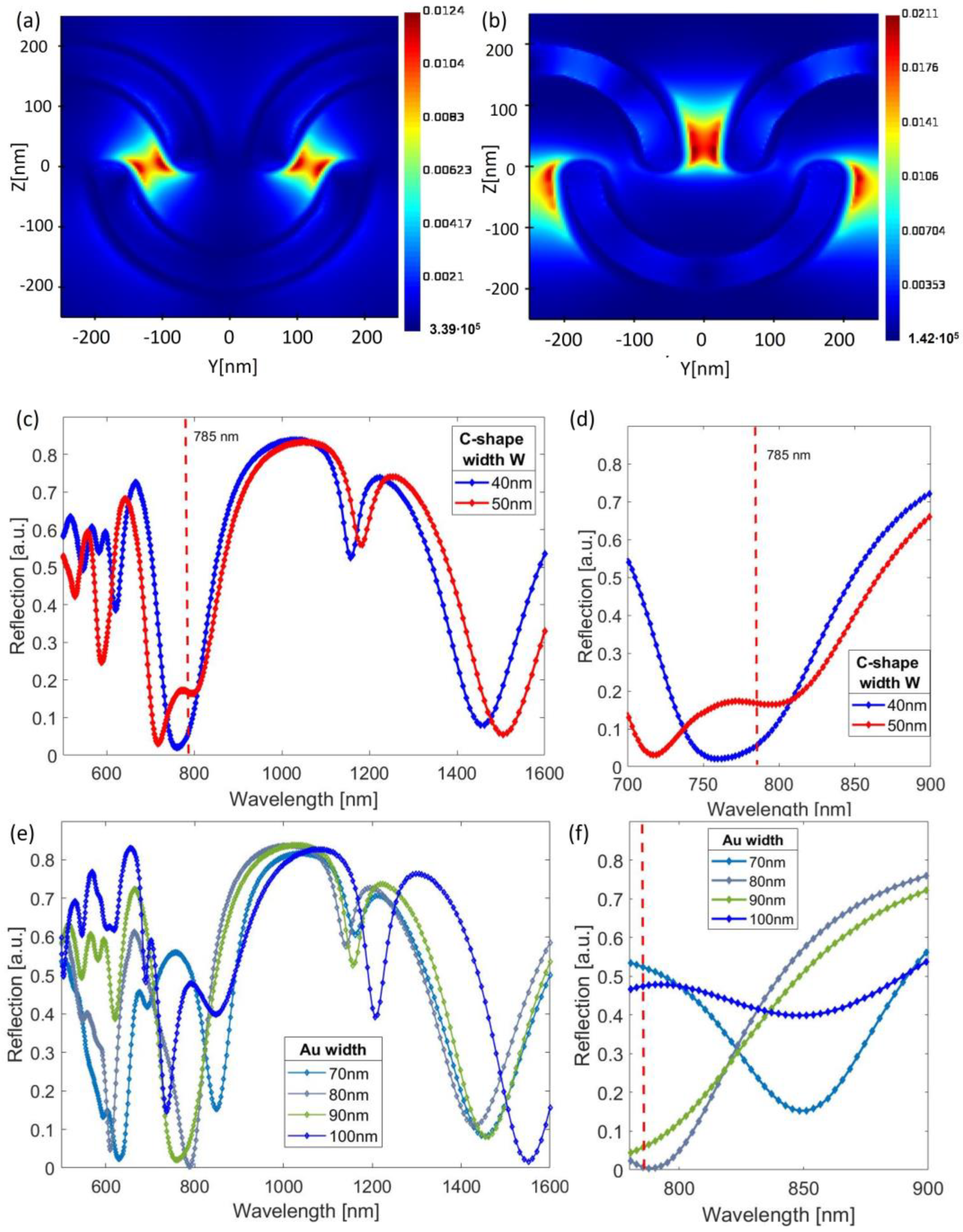
2. Design
3. Fabrication
4. Experimental Setup
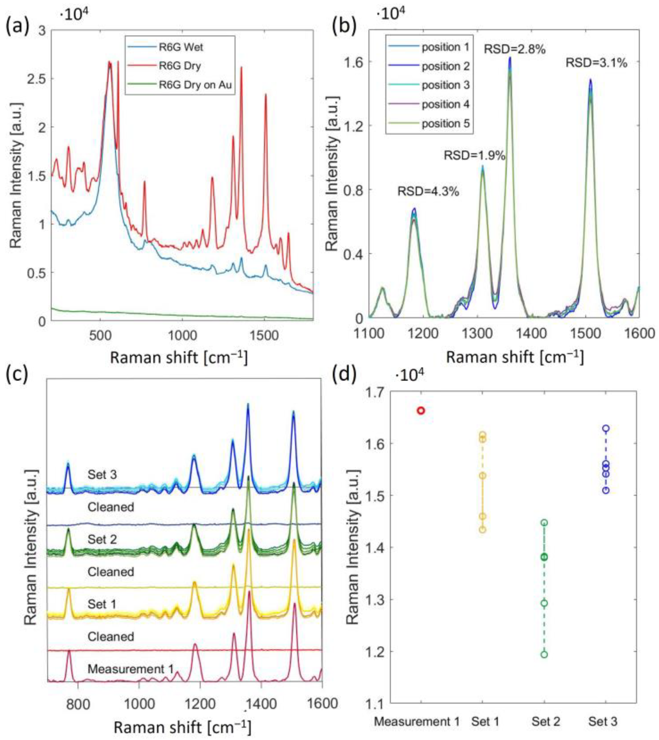
5. Results and Discussion
6. Conclusions
Author Contributions
Funding
Data Availability Statement
Conflicts of Interest
References
- Langer, J.; de Aberasturi, D.J.; Aizpurua, J.; Alvarez-Puebla, R.A.; Auguié, B.; Baumberg, J.J.; Bazan, G.C.; Bell, S.E.J.; Boisen, A.; Brolo, A.G.; et al. Present and future of surface-enhanced Raman scattering. ACS Nano 2020, 14, 28–117. [Google Scholar] [CrossRef] [PubMed]
- Tang, J.; Chen, W.; Ju, H. Rapid detection of pesticide residues using a silver nanoparticles coated glass bead as nonplanar substrate for SERS sensing. Sens. Actuators B Chem. 2019, 287, 576–583. [Google Scholar] [CrossRef]
- Moldovan, R.; Milenko, K.; Vereshchagina, E.; Iacob, B.C.; Schneider, K.; Farcău, C.; Bodoki, E. EC-SERS detection of thiabendazole in apple juice using activated screen-printed electrodes. Food Chem. 2023, 405, 134713. [Google Scholar] [CrossRef] [PubMed]
- Chisanga, M.; Muhamadali, H.; Ellis, D.I.; Goodacre, R. Enhancing disease diagnosis: Biomedical applications of surface-enhanced raman scattering. Appl. Sci. 2019, 9, 1163. [Google Scholar] [CrossRef]
- Pang, S.; Yang, T.; He, L. Review of surface enhanced Raman spectroscopic (SERS) detection of synthetic chemical pesticides. TrAC-Trends Anal. Chem. 2016, 85, 73–82. [Google Scholar] [CrossRef]
- Pérez-Jiménez, A.I.; Lyu, D.; Lu, Z.; Liu, G.; Ren, B. Surface-enhanced Raman spectroscopy: Benefits, trade-offs and future developments. Chem. Sci. 2020, 11, 4563–4577. [Google Scholar] [CrossRef]
- Shi, R.; Liu, X.; Ying, Y. Facing Challenges in Real-Life Application of Surface-Enhanced Raman Scattering: Design and Nanofabrication of Surface-Enhanced Raman Scattering Substrates for Rapid Field Test of Food Contaminants. J. Agric. Food Chem. 2018, 66, 6525–6543. [Google Scholar] [CrossRef]
- Bell, S.E.J.; Charron, G.; Cortés, E.; Kneipp, J.; Lamy, M.; Chapelle, D.; Langer, J.; Proch, M.; Tran, V.; Schl, S. Towards Reliable and Quantitative Surface-Enhanced Raman Scattering (SERS): From Key Parameters to Good Analytical Practice Angewandte. Angew. Chem. Int. Ed. Engl. 2020, 59, 5454–5462. [Google Scholar] [CrossRef]
- Grys, D.; Baumberg, J.J. Eliminating irreproducibility in SERS substrates. J. Raman Spectrosc. 2020, 52, 412–419. [Google Scholar] [CrossRef]
- Liu, Y.; Zhang, Y.; Tardivel, M.; Lequeux, M.; Chen, X.; Liu, W.; Huang, J.; Tian, H.; Liu, Q.; Huang, G.; et al. Evaluation of the Reliability of Six Commercial SERS Substrates. Plasmonics 2020, 15, 743–752. [Google Scholar] [CrossRef]
- Hou, L.; Shao, M.; Li, Z.; Zhao, X.; Liu, A.; Zhang, C.; Xiu, X.; Yu, J.; Li, Z. Elevating the density and intensity of hot spots by repeated annealing for high-efficiency SERS. Opt. Express 2020, 28, 29357. [Google Scholar] [CrossRef] [PubMed]
- Radziuk, D.; Moehwald, H. Prospects for plasmonic hot spots in single molecule SERS towards the chemical imaging of live cells. Phys. Chem. Chem. Phys. 2015, 17, 21072–21093. [Google Scholar] [CrossRef] [PubMed]
- Shvalya, V.; Filipič, G.; Zavašnik, J.; Abdulhalim, I.; Cvelbar, U. Surface-enhanced Raman spectroscopy for chemical and biological sensing using nanoplasmonics: The relevance of interparticle spacing and surface morphology. Appl. Phys. Rev. 2020, 7, 031307. [Google Scholar] [CrossRef]
- Yue, W.; Gong, T.; Long, X.; Kravets, V.; Gao, P.; Pu, M.; Wang, C. Sensitive and reproducible surface-enhanced raman spectroscopy (SERS) with arrays of dimer-nanopillars. Sens. Actuators B Chem. 2020, 322, 128563. [Google Scholar] [CrossRef]
- Wuytens, P.C.; Skirtach, A.G.; Baets, R. On-chip surface-enhanced Raman spectroscopy using nanosphere-lithography patterned antennas on silicon nitride waveguides. Opt. Express 2017, 25, 12926. [Google Scholar] [CrossRef]
- Luo, S.; Mancini, A.; Wang, F.; Liu, J.; Maier, S.A.; De Mello, J.C. High-Throughput Fabrication of Triangular Nanogap Arrays for Surface-Enhanced Raman Spectroscopy. ACS Nano 2021, 16, 7438–7447. [Google Scholar] [CrossRef]
- Darvill, D.; Iarossi, M.; Abraham Ekeroth, R.M.; Hubarevich, A.; Huang, J.A.; De Angelis, F. Breaking the symmetry of nanosphere lithography with anisotropic plasma etching induced by temperature gradients. Nanoscale Adv. 2021, 3, 359–369. [Google Scholar] [CrossRef] [PubMed]
- Cottat, M.; Lidgi-Guigui, N.; Tijunelyte, I.; Barbillon, G.; Hamouda, F.; Gogol, P.; Aassime, A.; Lourtioz, J.M.; Bartenlian, B.; de la Chapelle, M.L. Soft UV nanoimprint lithography-designed highly sensitive substrates for SERS detection. Nanoscale Res. Lett. 2014, 9, 623. [Google Scholar] [CrossRef] [PubMed]
- Wu, W.; Hu, M.; Ou, F.S.; Li, Z.; Williams, R.S. Cones fabricated by 3D nanoimprint lithography for highly sensitive surface enhanced Raman spectroscopy. Nanotechnology 2010, 21, 255502. [Google Scholar] [CrossRef]
- Barcelo, S.J.; Wu, W.; Li, X.; Li, Z.; Williams, R.S. Nanoimprint lithography of plasmonic platforms for SERS applications. Appl. Phys. A Mater. Sci. Process. 2015, 121, 443–449. [Google Scholar] [CrossRef]
- Alvarez-Puebla, R.; Cui, B.; Bravo-Vasquez, J.-P.; Veres, T.; Fenniri, H. Nanoimprinted SERS-Active Substrates with Tunable Surface Plasmon Resonances. J. Phys. Chem. C 2007, 111, 6720–6723. [Google Scholar] [CrossRef]
- Farcau, C.; Marconi, D.; Colniță, A.; Brezeștean, I.; Barbu-Tudoran, L. Gold nanopost-shell arrays fabricated by nanoimprint lithography as a flexible plasmonic sensing platform. Nanomaterials 2019, 9, 1519. [Google Scholar] [CrossRef] [PubMed]
- Jiang, S.; Espulgar, W.V.; Luo, X.; Saito, M.; Yoshikawa, H.; Tamiya, E. SERS active hierarchical nanopillar-huddle array fabricated via the combination of nanoimprint lithography and anodization. Electrochemistry 2020, 88, 165–173. [Google Scholar] [CrossRef]
- Cai, J.; Liu, R.; Jia, S.; Feng, Z.; Lin, L.; Zheng, Z.; Wu, S.; Wang, Z. SERS hotspots distribution of the highly ordered noble metal arrays on flexible substrates. Opt. Mater. 2021, 122, 111779. [Google Scholar] [CrossRef]
- Zhu, X.; Czolkos, I.; Johansson, A.; Nielsen, T.; Kristensen, A. Master origination by 248 nm DUV lithography for plasmonic color generation. Appl. Phys. Lett. 2021, 118, 141103. [Google Scholar] [CrossRef]
- Palik, E.D. Handbook of Optical Constants of Solids; Academic Press: Cambridge, MA, USA, 1998; Volume 3. [Google Scholar]
- Haynes, C.L.; Van Duyne, R.P. Plasmon-sampled surface-enhanced Raman excitation spectroscopy. J. Phys. Chem. B 2003, 107, 7426–7433. [Google Scholar] [CrossRef]
- Stuart, D.A.; Yonzon, C.R.; Zhang, X.; Lyandres, O.; Shah, N.C.; Glucksberg, M.R.; Walsh, J.T.; Van Duyne, R.P. Glucose sensing using near-infrared surface-enhanced raman spectroscopy: Gold surfaces, 10-day stability, and improved accuracy. Anal. Chem. 2005, 77, 4013–4019. [Google Scholar] [CrossRef]
- Mikac, L.; Kovačević, E.; Ukić, Š.; Raić, M.; Jurkin, T.; Marić, I.; Gotić, M.; Ivanda, M. Detection of multi-class pesticide residues with surface-enhanced Raman spectroscopy. Spectrochim. Acta-Part A Mol. Biomol. Spectrosc. 2021, 252, 119478. [Google Scholar] [CrossRef]
- Le Ru, E.C.; Blackie, E.; Meyer, M.; Etchegoint, P.G. Surface enhanced raman scattering enhancement factors: A comprehensive study. J. Phys. Chem. C 2007, 111, 13794–13803. [Google Scholar] [CrossRef]
- Huzortey, A.A.; Anderson, B.; Owusu, A. Raman spectra recovery using a second derivative technique and range independent baseline correction algorithm. OSA Contin. 2021, 4, 2468. [Google Scholar] [CrossRef]


Disclaimer/Publisher’s Note: The statements, opinions and data contained in all publications are solely those of the individual author(s) and contributor(s) and not of MDPI and/or the editor(s). MDPI and/or the editor(s) disclaim responsibility for any injury to people or property resulting from any ideas, methods, instructions or products referred to in the content. |
© 2023 by the authors. Licensee MDPI, Basel, Switzerland. This article is an open access article distributed under the terms and conditions of the Creative Commons Attribution (CC BY) license (https://creativecommons.org/licenses/by/4.0/).
Share and Cite
Milenko, K.; Dullo, F.T.; Thrane, P.C.V.; Skokic, Z.; Dirdal, C.A. UV-Nanoimprint Lithography for Predefined SERS Nanopatterns Which Are Reproducible at Low Cost and High Throughput. Nanomaterials 2023, 13, 1598. https://doi.org/10.3390/nano13101598
Milenko K, Dullo FT, Thrane PCV, Skokic Z, Dirdal CA. UV-Nanoimprint Lithography for Predefined SERS Nanopatterns Which Are Reproducible at Low Cost and High Throughput. Nanomaterials. 2023; 13(10):1598. https://doi.org/10.3390/nano13101598
Chicago/Turabian StyleMilenko, Karolina, Firehun Tsige Dullo, Paul C. V. Thrane, Zeljko Skokic, and Christopher A. Dirdal. 2023. "UV-Nanoimprint Lithography for Predefined SERS Nanopatterns Which Are Reproducible at Low Cost and High Throughput" Nanomaterials 13, no. 10: 1598. https://doi.org/10.3390/nano13101598
APA StyleMilenko, K., Dullo, F. T., Thrane, P. C. V., Skokic, Z., & Dirdal, C. A. (2023). UV-Nanoimprint Lithography for Predefined SERS Nanopatterns Which Are Reproducible at Low Cost and High Throughput. Nanomaterials, 13(10), 1598. https://doi.org/10.3390/nano13101598