Article

Compact Ga2O3 Thin Films Deposited by Plasma Enhanced Atomic Layer Deposition at Low Temperature

1
School of Opto-Electronic and Communication Engineering, Xiamen University of Technology, Xiamen 361024, China
2
Fujian Key Laboratory of Optoelectronic Technology and Devices, Xiamen University of Technology, Xiamen 361024, China
3
Department of Materials Science and Engineering, Da-Yeh University, Dacun, Changhua 51591, Taiwan
4
Department of Applied Materials and Optoelectronic Engineering, National Chi Nan University, Nantou 54561, Taiwan
5
Fujian Provincial Key Laboratory of Nanomaterials, Fujian Institute of Research on the Structure of Matter, Chinese Academy of Sciences, Fuzhou 350002, China
6
National Measurement and Testing Center for Flat Panel Display Industry, Xiamen Institute of Measurement and Testing, Xiamen 361004, China
*
Author to whom correspondence should be addressed.
Nanomaterials 2022, 12(9), 1510; https://doi.org/10.3390/nano12091510
Submission received: 4 April 2022 / Revised: 18 April 2022 / Accepted: 27 April 2022 / Published: 29 April 2022

Abstract

:
Amorphous Gallium oxide (Ga2O3) thin films were grown by plasma-enhanced atomic layer deposition using O2 plasma as reactant and trimethylgallium as a gallium source. The growth rate of the Ga2O3 films was about 0.6 Å/cycle and was acquired at a temperature ranging from 80 to 250 °C. The investigation of transmittance and the adsorption edge of Ga2O3 films prepared on sapphire substrates showed that the band gap energy gradually decreases from 5.04 to 4.76 eV with the increasing temperature. X-ray photoelectron spectroscopy (XPS) analysis indicated that all the Ga2O3 thin films showed a good stoichiometric ratio, and the atomic ratio of Ga/O was close to 0.7. According to XPS analysis, the proportion of Ga3+ and lattice oxygen increases with the increase in temperature resulting in denser films. By analyzing the film density from X-ray reflectivity and by a refractive index curve, it was found that the higher temperature, the denser the film. Atomic force microscopic analysis showed that the surface roughness values increased from 0.091 to 0.187 nm with the increasing substrate temperature. X-ray diffraction and transmission electron microscopy investigation showed that Ga2O3 films grown at temperatures from 80 to 200 °C were amorphous, and the Ga2O3 film grown at 250 °C was slightly crystalline with some nanocrystalline structures.

1. Introduction

Gallium oxide (Ga2O3) thin film has attracted wide attention owing to its wide band gap, high breakdown electric field, and high optical transparency. It has been applied to some high-performance devices, such as deep ultraviolet light detectors [1,2], photodiodes [3,4], and transparent field effect tubes [5,6]. Ga2O3 is a kind of oxide semiconductor material; it has a variety of crystal phases, including α, β, γ, δ, ε. The most stable and widely studied phase is the β-Ga2O3 phase. The other metastable phases can be transformed into relatively stable β-Ga2O3 after high-temperature thermal annealing. There are many methods to prepare Ga2O3 thin film, such as radio frequency (RF) [7,8] magnetron sputtering, pulsed laser deposition (PLD) [9,10], molecular beam epitaxy (MBE) [11,12], metal-organic chemical vapor deposition (MOCVD) [13,14], and atomic layer deposition (ALD) [15,16,17]. Although magnetron sputtering and PLD can prepare Ga2O3 thin films on a relatively low-temperature substrate, the most obvious shortcoming is that the film surface cannot show a large area of uniformity, and the crystal quality needs further improvement. Ga2O3 films prepared by MBE and MOCVD need to be carried out at a relatively high substrate temperature, such as 700–1000 °C. Compared with other deposition methods, ALD is considered to be one of the most advantageous deposition methods because of its good thickness control and uniform film growth. In addition, compared with traditional ALD, plasma-enhanced atomic layer deposition (PEALD) can improve the crystallinity of the film and enhance the effect of plasma in the whole ALD reaction process. It can have better control of the film’s growth in lower temperature environments and reduces the heat load in the reaction. Therefore, PEALD is widely used in film growth. Studying the properties of Ga2O3 films prepared by PEALD at a low temperature is a popular topic. For example, Dong-Won Choi et al. deposited Ga2O3 film by ALD at a low deposition temperature (150–250 °C) using gallium tri-isopropoxide (GTIP) as the gallium source and H2O as the oxygen source. The growth rate of Ga2O3 film increased sharply and saturated to 0.25 nm/cycle [18]. Using trimethylgallium (tmga) and ozone (O3), Daniel Hiller et al. observed that Ga2O3 growth per cycle (GPC) was ~0.4 Å/cycle and ~0.5 Å/cycle in thermal ALD at 250 °C and 300 °C. The GPC of Ga2O3 reaches ~0.7 Å/cycle in PEALD at 75 °C [17]. It can be seen that PEALD can obtain a higher deposition rate using a lower deposition temperature than that of thermal ALD. There also have been many reports about the selection of precursors. Saidjafarzoda Ilhom et al. prepared Ga2O3 films using trethylgallium (TEG) and Ar/O2 as the precursor system. The substrate temperature range was 150–240 °C, and the RF plasma range was 30–300 W. The GPC of the film ranged from 0.69 to 1.31 Å/cycle [19]. The precursors used by Ramachandran et al. were Gallium tetramethylheptanedionate (Ga(tmhd)3) and oxygen. They prepared the films in the temperature range of 100–400 °C and an RF power of 300 W. Under these conditions, the film growth rate was 0.1 Å/cycle [20].
In this study, Ga2O3 films were prepared using tmga and oxygen as precursors through PEALD at a plasma power of 2500 W. The substrate temperature varied from 80 to 250 °C. The growth temperature effect on optical properties, surface morphology, chemical element distribution, and structural properties of the deposited PEALD Ga2O3 film were comprehensively studied. The effects of different substrate temperatures on the deposition mechanism and properties of Ga2O3 thin films were discussed to obtain high-density Ga2O3 thin films with few defects.

2. Materials and Methods

In this work, sapphire and silicon were used as deposition substrates. The sapphire substrate was cleaned with deionized water, ethanol, isopropyl alcohol, and deionized water for 15 min in sequence, respectively. The sapphire substrates were then blown by N2 and transferred to a vacuum drying cabinet for more than 20 min in order to remove water vapor. For the Si substrates, they were cleaned through a standard Radio Corporation of American (RCA) cleaning process and then soaked in 2% hydrogen fluoride solution for 1 min to remove the surface natural oxide layer. They were then cleaned in deionized water and finally dried with an N2 gas gun. After cleaning, the substrates were transferred into the ALD reaction chamber. Ga2O3 films were deposited on different substrates (Si and sapphire) at 80, 100, 150, 200, and 250 °C using tmga and oxygen plasma at 2500 W in a commercial PEALD system (Picosun R-200, Espoo, Finland). The plasmas were produced in a microwave cavity using inductive coupling of RF power (Litmas RPS, Advanced Energy, Denver, CO, USA) with the mixture of Ar and O2 gases, which belonged to a high-density remote plasma system. According to our previous experimental study [21,22], 2500 W can form high-density oxygen free radicals, which enables it to carry out a good oxidation saturation reaction and avoid plasma bombardment on the surface of the film. Therefore, high-density and high-quality gallium oxide films can be obtained at the power of 2500 W. N2 gas was used as the carrier gas with the flow rates of 120 sccm for tmga. Tmga was stored at 0 °C in stainless bottles. The deposition process of PEALD Ga2O3 sequentially included: tmga pulse time (0.2 s)-N2 purge time (4 s)-O2 plasma processing (28 s)-N2 purge time (4 s). During the deposition, the total number of cycles for all the samples is 600. Table 1 is a list of the growth parameters of the PEALD Ga2O3 films.
The thickness and refractive index of the Ga2O3 films deposited on silicon wafers were characterized by a spectroscopic ellipsometer (SE, SENTECH SE 800 DUV, Berlin, Germany). The refractive index of the Ga2O3 thin films was obtained from the SE characterization assuming a Tauc–Lorentz model. The optical transmittance of the films deposited on the sapphire substrates was obtained by a UV-vis spectrophotometer (Lambda850, PerkinElmer, Waltham, MA, USA) at a wavelength between 200 and 800 nm at room temperature. The structural properties of the Ga2O3 films were examined by conventional θ-2θ X-ray diffraction (XRD, Rigaku TTRAXIII, Ibaraki, Japan) using a copper Kα emission line. The chemical compositions and bonding states were characterized by X-ray photoelectron spectroscopy (XPS, ESCALAB 250Xi, Thermo Fisher, Waltham, MA, USA). The size of the Ga2O3 films for XPS measurement is 5 × 5 mm2. Ga2O3 films were fixed on the XPS test bench using conducting resin. Non-test surfaces of the Ga2O3 films were marked and distinguished from test ones. The total acquisition time was 136.1 s. XPS measurements were recorded using monochromatized Al K Alpha as the excitation source with a spot size of 400 µm2. According to the reported literature [23], the chemical state of Ga could not be changed after Ar+ pre-sputtering on the sample’s surface. Nevertheless, a few other reports [24,25,26] inferred that the introduced Ar+ bombardment had a crucial effect on the oxidation states. Hence, in order to eliminate the influence of Ar+ pre-etch on the formation of lower Ga oxidation valence states, the XPS measurements were executed without Ar+ pre-sputtering. The thickness of the Ga2O3 thin films was also determined by X-ray reflectivity (XRR, Rigaku TTRAXIII, Ibaraki, Japan) and HR-S/TEM (FEI Talos F200X, Hillsboro, OR, USA). XRR is a nondestructive technique frequently used for measuring the thickness, density, and roughness of thin films [27]. The crystal structure and interfacial layers of the Ga2O3 thin films were investigated by HR-S/TEM. Energy dispersive X-ray (EDX) analysis for the elemental mapping of the Ga2O3 thin films was performed with the same instrument.

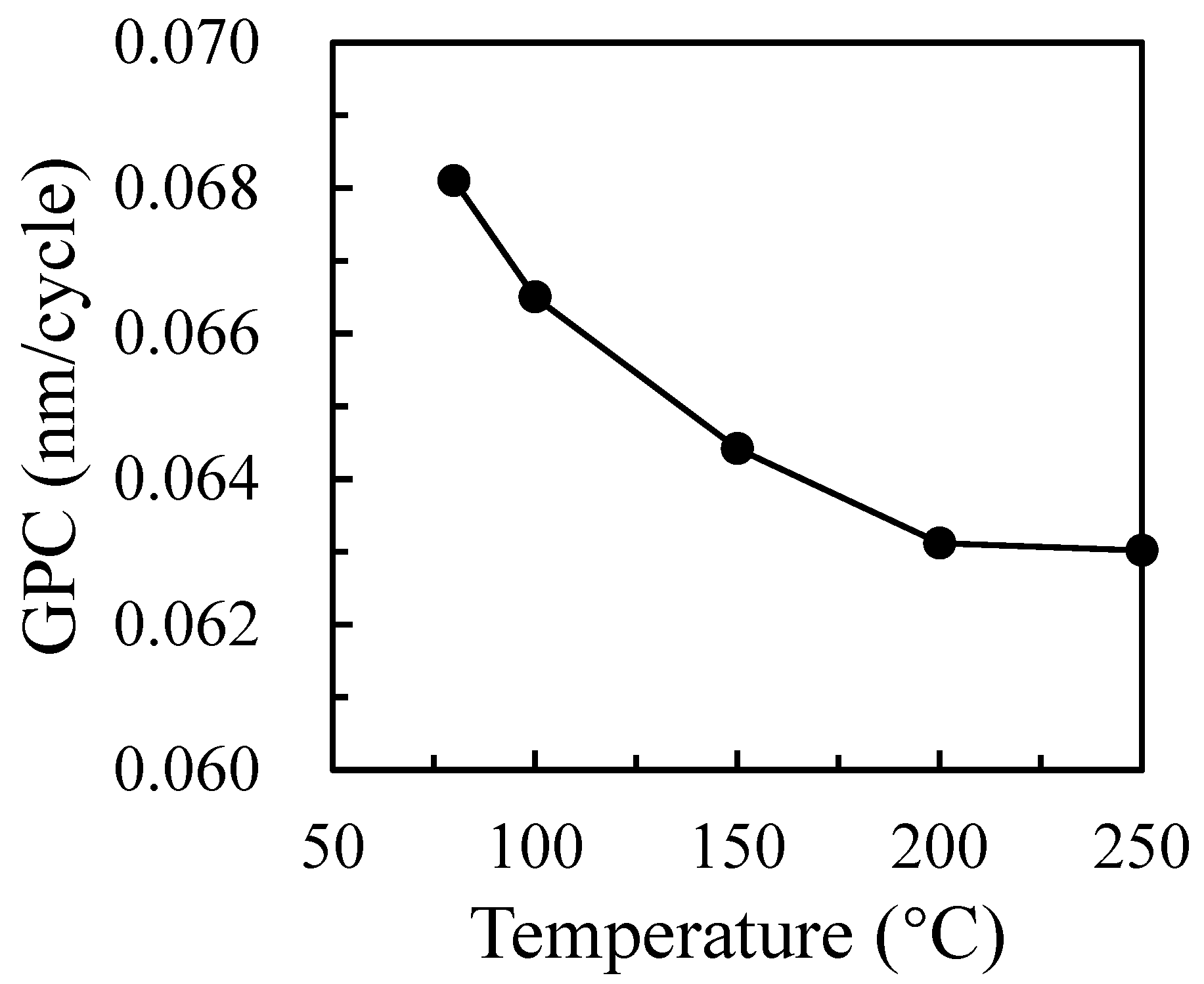
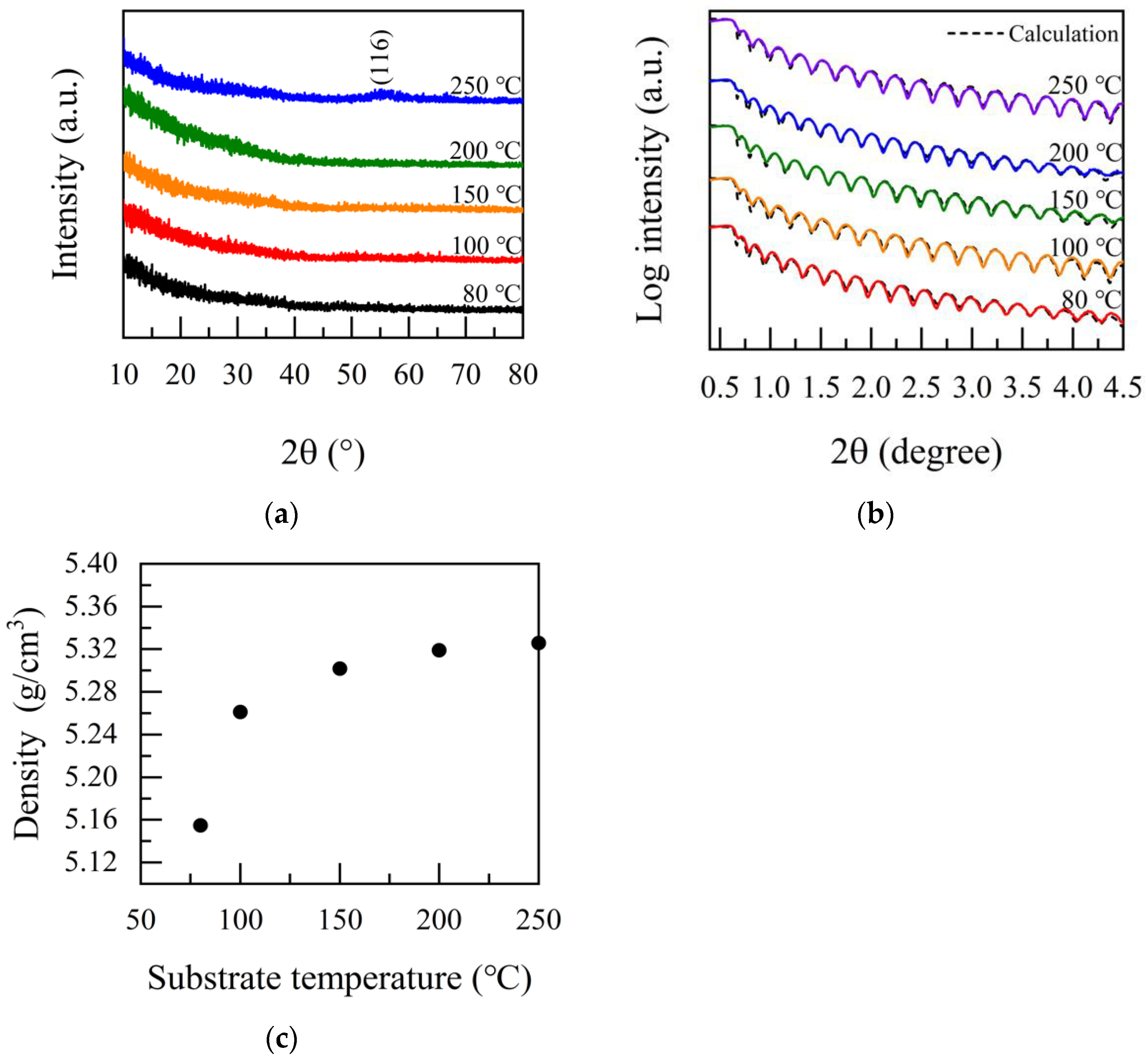
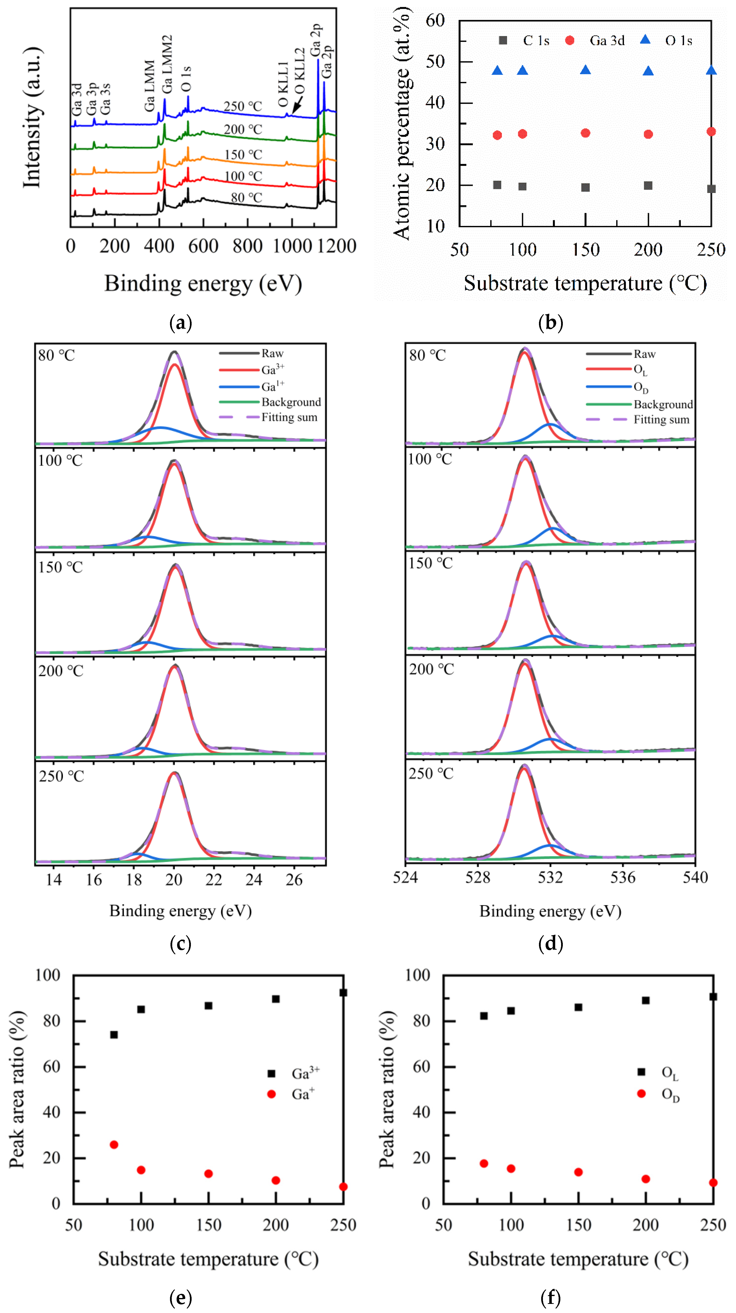
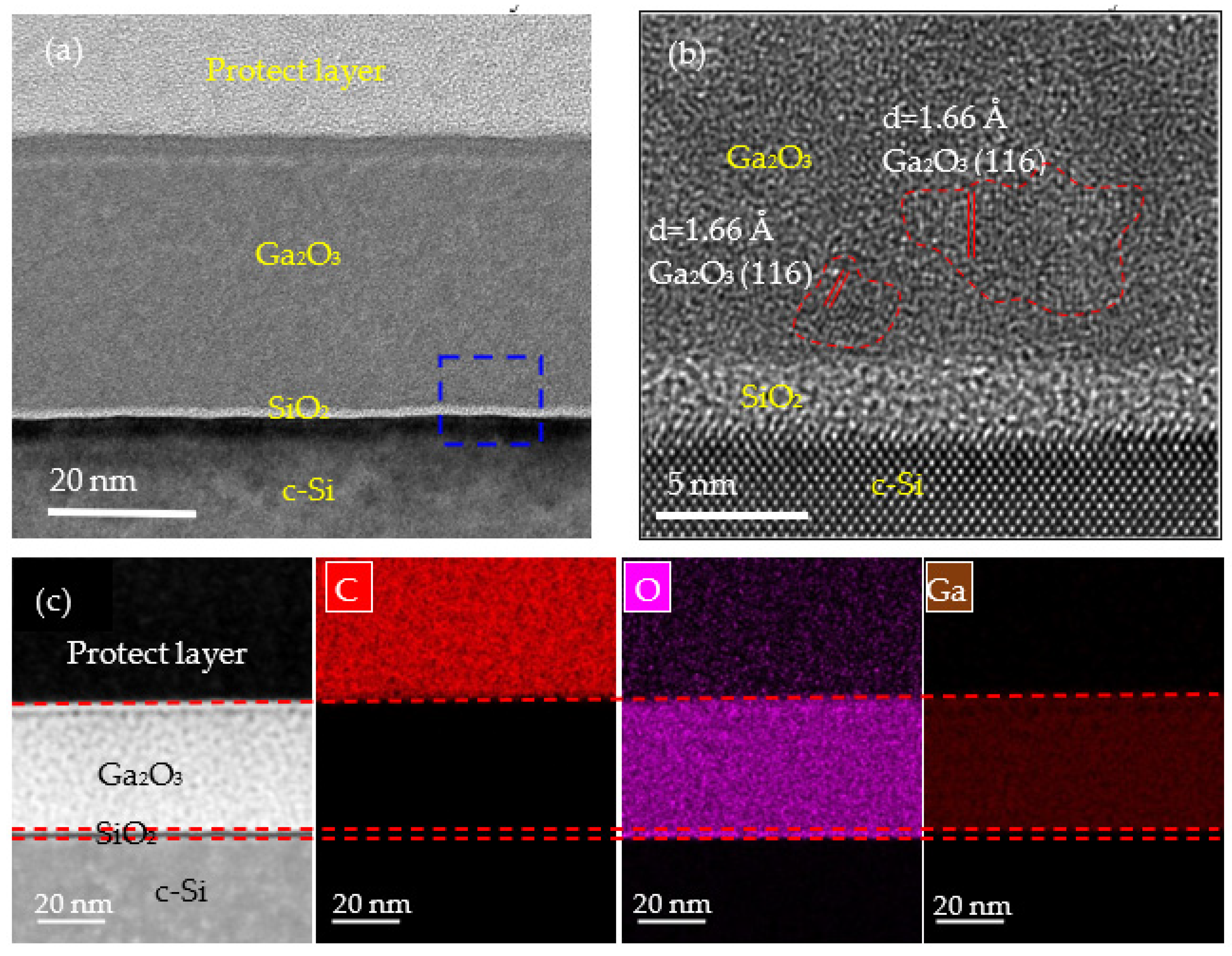
3. Results and Discussion

Figure 1 shows the changes in the film’s GPC with a substrate temperature from 80 °C to 250 °C. The GPC is defined as the thickness divided by the number of cycles. The thickness of the Ga2O3 films prepared at the 600 cycles with a substrate temperature varying from 80 °C to 250 °C is 40.86, 39.90, 38.65, 37.87, and 37.81 nm, respectively. It can be seen that the change of thickness is not obvious, but the GPC of the film gradually decreases and tends to saturate with the increase in substrate temperature to 200 °C. When the temperature is 80 °C, the film is the thickest, corresponding to the largest deposition rate of 0.068 nm/cycle. When the growth temperature increases to 200 °C, the GPC decreases to 0.063 nm/cycle, as shown in Figure 1. Therefore, the substrate temperature has little effect on the deposition rate, which ranges in GPC from 0.068 nm/cycle to 0.063 nm/cycle when the substrate temperature is 80–250 °C. This phenomenon may be related to the physical and chemical adsorption of the precursor. Some precursors have a low activity due to a low temperature. The higher growth rate observed below 100 °C may be due to precursor condensation onto the substrate or the incomplete removal of the reaction by-products at low temperatures, giving rise to some organic residues from the precursor ligands incorporated into the film [20]. On the other hand, it is caused by chemisorption. In this study, the precursor chemical reaction can be elaborated by the following equations:
Si-OH + Ga(CH3)3 → Si-O-Ga(CH3)2 + CH4
Si-O-Ga(CH3)2 + O* → Si-O-Ga-OH + CO2 + H2O
It is known that the precursor of Ga(CH3)3 reacts with a hydroxyl group on the surface of a silicon wafer to decompose into Si-O-Ga(CH3)2 and CH4 gas in the whole ALD reaction system. When O2 plasma participates in the second semi-reaction, Ga2O3 is generated. Therefore, the precursor may condense because of the low deposition temperature resulting in a high deposition rate. As the substrate temperature rises, the desorption ability between the precursor and the deposition surface will be enhanced, which will cause a decrease in the deposition rate.
Figure 2a shows the XRD patterns of the Ga2O3 films prepared at various substrate temperatures. No obvious peaks were detected in the deposited Ga2O3 film at the temperature of 80–200 °C, indicating that the Ga2O3 films are uncrystallized or contain some localized microstructure, such as nano-crystals. The amorphous characteristics of the films can be attributed to the low growth temperature [8,28]. At the same time, it is found that there is slight crystallization in the film at 250 °C. By comparing PDF#06-0503, it can be seen that there is a broad peak at 55.114°, corresponding to the (116) crystallization plane of the α-Ga2O3 film. The density of Ga2O3 films was measured by XRR. Figure 2b shows the XRR pattern of β-Ga2O3 films. The density of the Ga2O3 thin films as a function of growth temperature is shown in Figure 2c. The film density increases with the increase in the growth temperature. It is noteworthy that the density decreased to 5.154 g/cm3 at 80 °C due to insufficient surface reaction. With the continuous increment of deposition temperature, the density gradually increased. The highest density of 5.325 g/cm3 was achieved at 250 °C, which was slightly lower than the β-Ga2O3 bulk density of 5.95 g/cm3 [29,30]. As demonstrated below, the ALD deposited on the Ga2O3 films were amorphous, leading to a lower density [8]. Compared with the previously reported Ga2O3 density of 5.95 g/cm3 prepared by edge-defined film-fed growth (EFG) [30], the density of Ga2O3 film is lower, which is on account of the non-crystalline structure of Ga2O3 film prepared by ALD process [28]. The density of Ga2O3 prepared by Z. Yu et al. using MBE was 5.3 g/cm3 [31]. The density of Ga2O3 prepared by M. Passlack et al. using the electron—beam specific fuel was 5.15 g/cm3 [32]. Nieminen et al. prepared a Ga2O3 film by atomic layer epitaxy, with Ga(acac)3 and ozone as the precursor system. They found that the density of the film is 5.6 g/cm3 [33]. The density of β-Ga2O3 measured by Richard et al. was 5.12 g/cm3 [34]. It can be seen that the density of Ga2O3 film grown in this study is within the theoretical range and superior to ordinary deposition techniques. In Table 2, a comparison has been made for the properties of Ga2O3 films prepared by different methods. Compared with other methods, the Ga2O3 films deposited by PEALD have a higher film density, which is also slightly better than the results in Ref. [34]. Moreover, the roughness of the film in Ref. [34] is 0.31–0.44 nm, while the roughness in our study is only 0.187 nm. Therefore, the gallium oxide film prepared in this study had a relatively high density with a very smooth surface.
The chemical valence state and composition of Ga2O3 thin films were analyzed by XPS measurements. Figure 3a shows the investigation spectra of the deposited Ga2O3 films at different substrate temperatures. The spectra were mainly marked with peaks associated with Ga, such as Ga 3s, Ga 3p, Ga 3d, Ga 2p1/2, and Ga 2p3/2, as well as peaks associated with O, such as O 1s and O 2s, respectively. The auger of Ga (Ga LMM) and oxygen (O KLL) were also observed in the figure. Figure 3b represents the atomic ratio of Ga 3d, O 1s, and C 1s for Ga2O3 films with the variation of substrate temperatures. From the figure, it can be seen that the percentage of O 1s element was nearly 50% and more than 30% for the Ga element. The C element was slightly high because there was no Ar etching before the measurement. The Ga/O ratio of all the films is about 0.7, which is close to the stoichiometric ratio of Ga2O3 and consistent with the report [28] of 0.71.
Ga 3d high-resolution XPS spectra taken from the surface of Ga2O3 films were fitted with two subpeaks, which are shown in Figure 3c. Ga 3d located at 20.54 eV is a typical value for Ga-O bonding in β-Ga2O3. The binding energies of the oxidation valence state of Ga3+ and Ga+ are 19.98~20.18 eV and 18.08–19.38 eV, respectively. Ga3+ corresponds to a high oxidation state in the film, while Ga+ relates to a low oxidation state [23], as shown in Figure 3c. The proportion of Ga3+ increases with the increase in substrate temperature and reaches the highest value of 92.42% at 250 °C. It indicates that the film quality gets better and better with the increase in substrate temperature. Figure 3d shows the core O1s energy level spectra of Ga2O3 films. The fitting is divided into two peaks. The binding energy at 530.7 eV conforms to the chemical bonding state of the Ga2O3 film, namely lattice oxygen (OL). Moreover, the other peak located at 531.3 eV [35] is due to oxygen deficiency (OD). Figure 3e,f shows the peak area ratio of Ga3+, Ga+, OL, and OD, respectively. When the substrate temperature rises from 80 to 250 °C, the proportion of OL increases from 82.27% to 87.05%, and the proportion of OD decreases from 17.73% to 12.95%. When the substrate temperature is low, oxygen does not have enough energy to fully react with tmga, resulting in a high ratio of oxygen deficiency [35], which is a signal from lattice oxygen in the vicinity of lower valence cation or in the vicinity of oxygen vacancy. The increase in substrate temperature is beneficial for reducing the defects in Ga2O3 film. The higher the substrate temperature, the fewer the defects in the films. Hao Liu et al. [35] grew β-Ga2O3 thin films by PLD. When the oxygen pressure was 0.01 Pa, the lattice oxygen content in the films was 87.06%, and the Ga3+ content was 92.53%, which were close to the results obtained in our study. The Ga2O3 film prepared using PLD by HongYang [36] et al. under the condition of 400 °C has 79.5% Ga-O content and ~20.5% C-O content. The Ga content of Ga2O3 is 91.9%. Yancheng Chen et al. [37] prepared Ga2O3 films on c-plane sapphire substrates using a plasma-enhanced chemical vapor deposition technique; they reported that the lowest oxygen deficiency ratio was 27.8%. Obviously, the Ga2O3 film prepared in this study possesses a low defect density, which is superior to the above preparation methods.
Figure 4 is the SEM images of the top view of Ga2O3 thin film. The images show that Ga2O3 films grown at different substrate temperatures are very smooth. Moreover, the AFM measurement was further used to investigate the roughness of the films. The AFM images were inset on the top right corner of the SEM images. Although the film is smooth and mostly in an amorphous state [34], it can still be found that the root mean square roughness (Rq) of the Ga2O3 thin film increases from 0.091 to 0.187 nm with the increase in substrate temperature [38]. Combined with XRR measurements, the Ga2O3 surface is relatively smooth. Compared with the roughness of the Ga2O3 film (about 0.8 nm) prepared by RF Sputtering [8], the smoother Ga2O3 film can be obtained in this study.
Figure 5 shows the cross-sectional TEM images of the PEALD Ga2O3 film prepared at 250 °C. In Figure 5a, a sandwich structure can be observed, which consists of three regions: the Ga2O3 layer, interfacial oxide SiO2, and Si substrate. According to the study by H. Altuntas et al. [39], a very thin SiO2 layer at the Si/Ga2O3 interface was formed. Many researchers have illustrated that Ga2O3 films deposited by PEALD at the window temperatures were amorphous. Inci Donmez et al. [40] pointed out that gallium oxide prepared by PEALD at 28–400 °C was amorphous when the film was deposited at 250 °C. Richard O’Donoghue et al. [34] deposited Ga2O3 at 60–160 °C by PEALD and also reached the same conclusion. Ranjinth k. Ramachandran et al. [20] deposited gallium oxide films at 100–400 ℃, and all the films were amorphous. Compared with X. Li et al.’s [28] investigation of the deposition of Ga2O3 by PEALD, it is interesting to find that even within the same substrate temperature variation range, slight crystallization can be seen at 250 °C in our study through high resolution-scanning/transmission electron microscopy (HR-S/TEM) measurements. Therefore, PEALD deposition is difficult to form on highly crystalline Ga2O3 films. A highly compact Ga2O3 thin film with a thickness of about 38 nm can be observed, which is in good agreement with the ellipsometer measurement result. The film is dense without any observable vacancies or voids. Figure 5b illustrates a magnified micrograph of Figure 5a. It can be clearly seen that the deposited Ga2O3 thin films have some nanocrystalline structure. The lattice spacing of about 1.66 Å evaluated from the HR-S/TEM image corresponds to the (116) plane of the α-Ga2O3 film [41,42], which is in agreement with the result from the XRD measurements. The interface of Ga2O3/Si shows an amorphous SiO2 layer, which results from the O2 plasma radicals reacting with the substrate in the first few cycles. The structure of the interfacial SiO2 layer was also found in our previous studies and literature using PEALD to prepare metal oxide films on Si wafers [22,39]. Cross-assigned EDX elemental mapping of carbon (C), oxygen (O), and gallium (Ga) is shown in Figure 5c. From the image, the C signal is hard to find within the Ga2O3 layer. The O and Ga elements were uniformly distributed in the film.
Figure 6a shows the transmittance spectra of Ga2O3 films at various temperatures on the sapphire substrate. The transmittance spectra were measured in the wavelength of 200 to 800 nm. All of the Ga2O3 films display an excellent optical transmittance with a high average transmittance of more than 90% in the visible light range. The absorption edge presents a redshift with the increase in substrate temperature, which is concerned with the reduced band gap of the film. The band gap of the film was determined by spectrophotometry, which is shown in Figure 6b. The transmission spectrum is transformed into (αhν)2~, α is calculated by the Beer–Lambert law: α(λ) = ln(1/T(λ))/d, where T is the penetration rate, and d is the thickness of the film. By extrapolating the linear region of (αhν)2~ to the horizontal axis, the band gap of the film was obtained. Figure 6c shows the decreasing band gap from 5.04 to 4.76 eV with the increase in substrate temperature. Yancheng Chen et al. [37] reported that the band gap of the Ga2O3 film was between 4.4 eV and 5.1 eV. At lower substrate temperatures, the higher band gap value is attributed to the effect of excess O2 in the film or the presence of amorphous properties [43]. However, XPS results show that the ratio of Ga/O in the Ga2O3 film prepared in this experiment is slightly more than 0.7. The slight decrease in the band gap may be attributed to the high substrate temperature resulting in the formation of some nanocrystalline structures in the film.
Figure 6d shows the refractive index changes of the Ga2O3 films prepared at different substrate temperatures at different wavelengths. The refractive index curves of thin films were fitted by using the Tauc–Lorentz model. The obtained refractive index at 632.8 nm is 1.85~1.9, which is in good agreement with other reports using the same PEALD process [28,34,44]. The refractive index of amorphous Ga2O3 films increases gradually with the increase in substrate temperature due to the increasing density of Ga2O3 film. In the range of growth temperature, the higher the growth temperature is, the more favorable it is for the gaseous by-products to be desorbed and discharged from the surface so as to obtain a higher density film. XRR results also show that the film density increases with the increase in substrate temperature.

4. Conclusions

Ga2O3 thin films were deposited using tmga and oxygen plasma by PEALD in a substrate temperature range from 80 to 250 °C. The films present with an amorphous structure deposited at 80 to 200 °C, and they had a slight crystallization at 250 °C. XRR analysis of the film density found that the higher the temperature was, the denser the films were. According to XPS analysis, the proportion of Ga3+ and OL increases with the increase in temperature, which means the reduced defects of the film. Moreover, films with higher density and better quality can be obtained with the increase in temperature. Additionally, the band gap of the Ga2O3 thin films decreases with the increase in temperature. SEM and AFM results show that changing the substrate temperature has little effect on the surface morphology, and the surface of Ga2O3 films is smooth. HR-S/TEM images show that Ga2O3 films have some nanocrystalline structures corresponding to the (116) plane of the α-Ga2O3 film.

Author Contributions

Funding acquisition, S.-Y.L. and X.-Y.Z.; Y.Y., F.-B.R. and R.-F.Z. performed the experiments; data analyses, Y.Y., X.-Y.Z., C.W., S.-Y.L., C.-H.H., W.-Y.W., P.G., Y.-J.R., D.-S.W. and W.-Z.Z.; Y.Y. wrote the manuscript; S.-Y.L. revised and review the manuscript; supervision, S.-Y.L. All authors took part in the investigation and discussion. All authors have read and agreed to the published version of the manuscript.

Funding

This work is partially supported by the Science and Technology Project of Xiamen (No. 3502ZCQ20191002), the Natural Science Foundation of Fujian Province (Nos. 2020H0025, 2020J01298 and 2018J05115) and the Scientific project of Xiamen University of Technology (No. YKJ18008R). This work is also supported by the Xiamen Scientific Research Start-up Foundation for the Returned Overseas Chinese Scholars (No. 5010320004), the National Natural Science Foundation of China (No. 61904155) and the Science and Technology Projects of Fujian Administration for Market Regulation (FJMS2020044).

Institutional Review Board Statement

Not applicable.

Informed Consent Statement

Not applicable.

Data Availability Statement

No new data were created or analyzed in this study. Data sharing is not applicable to this article.

Conflicts of Interest

The authors declare that they have no competing interest.

References

  1. Pintor-Monroy, M.I.; Murillo-Borjas, B.L.; Quevedo-Lopez, M.A. Nanocrystalline and Polycrystalline β-Ga2O3 Thin Films for Deep Ultraviolet Detectors. ACS Appl. Electron. Mater. 2020, 2, 3358. [Google Scholar] [CrossRef]
  2. Oshima, T.; Okuno, T.; Arai, N.; Suzuki, N.; Ohira, S.; Fujita, S. Vertical Solar-Blind Deep-Ultraviolet Schottky Photodetectors Based on β-Ga2O3 Substrates. Appl. Phys. Express 2008, 1, 011202. [Google Scholar] [CrossRef]
  3. Nakagomi, S.; Sakai, T.; Kikuchi, K.; Kokubun, Y. β-Ga2O3/p-Type 4H-SiC Heterojunction Diodes and Applications to Deep-UV Photodiodes. Phys. Status Solidi A 2019, 216, 1700796. [Google Scholar] [CrossRef]
  4. Atilgan, A.; Yildiz, A.; Harmanci, U.; Gulluoglu, M.T.; Salimi, K. β-Ga2O3 Nanoflakes/p-Si Heterojunction Self-Powered Photodiodes. Mater. Today Commun. 2020, 24, 101105. [Google Scholar] [CrossRef]
  5. Hernandez, A.; Islam, M.M.; Saddatkia, P.; Codding, C.; Dulal, P.; Agarwal, S.; Janover, A.; Novak, S.; Huang, M.; Dang, T.; et al. MOCVD Growth and Characterization of Conductive Homoepitaxial Si-Doped Ga2O3. Results Phys. 2021, 25, 104167. [Google Scholar] [CrossRef]
  6. Wu, Z.; Jiang, Z.; Song, P.; Tian, P.; Hu, L.; Liu, R.; Fang, Z.; Kang, J.; Zhang, T. Nanowire-Seeded Growth of Single-Crystalline (010) β-Ga2O3 Nanosheets with High Field-Effect Electron Mobility and On/Off Current Ratio. Small 2019, 15, 1900580. [Google Scholar] [CrossRef]
  7. Singh, M.; Casbon, M.A.; Uren, M.J.; Pomeroy, J.W.; Dalcanale, S.; Karboyan, S.; Tasker, P.J.; Wong, M.H.; Sasaki, K.; Kuramata, A.; et al. Pulsed Large Signal RF Performance of Field-Plated Ga2O3 MOSFETs. IEEE Electron Device Lett. 2018, 39, 1572. [Google Scholar] [CrossRef] [Green Version]
  8. Singh, A.K.; Gupta, M.; Sathe, V.; Katharria, Y.S. Effect of Annealing Temperature on β-Ga2O3 Thin Films Deposited by RF Sputtering Method. Superlattices Microstruct. 2021, 156, 106976. [Google Scholar] [CrossRef]
  9. Yadav, M.K.; Mondal, A.; Das, S.; Sharma, S.K.; Bag, A. Impact of Annealing Temperature on Band-Alignment of PLD Grown Ga2O3/Si (100) Heterointerface. J. Alloys Compd. 2020, 819, 153052. [Google Scholar] [CrossRef]
  10. Shen, H.; Baskaran, K.; Yin, Y.; Tian, K.; Duan, L.; Zhao, X.; Tiwari, A. Effect of Thickness on the Performance of Solar Blind Photodetectors Fabricated Using PLD Grown β-Ga2O3 Thin Films. J. Alloys Compd. 2020, 822, 153419. [Google Scholar] [CrossRef]
  11. Sasaki, K.; Higashiwaki, M.; Kuramata, A.; Masui, T.; Yamakoshi, S. MBE Grown Ga2O3 and Its Power Device Applications. J. Cryst. Growth 2013, 378, 591. [Google Scholar] [CrossRef]
  12. Pratiyush, A.S.; Xia, Z.; Kumar, S.; Zhang, Y.; Joishi, C.; Muralidharan, R.; Rajan, S.; Nath, D.N. MBE-Grown β-Ga2O3-Based Schottky UV-C Photodetectors With Rectification Ratio ~107. IEEE Photonics Technol. Lett. 2018, 30, 2025. [Google Scholar] [CrossRef]
  13. Li, Z.; Jiao, T.; Yu, J.; Hu, D.; Lv, Y.; Li, W.; Dong, X.; Zhang, B.; Zhang, Y.; Feng, Z.; et al. Single Crystalline β-Ga2O3 Homoepitaxial Films Grown by MOCVD. Vacuum 2020, 178, 109440. [Google Scholar] [CrossRef]
  14. Cao, Q.; He, L.; Xiao, H.; Feng, X.; Lv, Y.; Ma, J. β-Ga2O3 Epitaxial Films Deposited on Epi-GaN/Sapphire (0001) Substrates by MOCVD. Mater. Sci. Semicond. Process. 2018, 77, 58. [Google Scholar] [CrossRef]
  15. Dezelah, C.; Niinistö, J.; Arstila, K.; Niinistö, L.; Winter, C.H. Atomic Layer Deposition of Ga2O3 Films from a Dialkylamido-Based Precursor. Chem. Mater. 2006, 18, 471. [Google Scholar] [CrossRef]
  16. Lee, S.H.; Lee, K.M.; Lee, S.W. Influences of Process Temperature on a Phase of Ga2O3 Thin Films Grown by Atomic Layer Deposition on Sapphire. Bull. Korean Chem. Soc. 2020, 41, 1190. [Google Scholar] [CrossRef]
  17. Hiller, D.; Julin, J.; Chnani, A.; Strehle, S. Silicon Surface Passivation by ALD-Ga2O3: Thermal vs. Plasma-Enhanced Atomic Layer Deposition. IEEE J. Photovolt. 2020, 10, 959. [Google Scholar] [CrossRef]
  18. Choi, D.; Chung, K.-B.; Park, J.-S. Low Temperature Ga2O3 Atomic Layer Deposition Using Gallium Tri-Isopropoxide and Water. Thin Solid Films 2013, 546, 31. [Google Scholar] [CrossRef]
  19. Ilhom, S.; Mohammad, A.; Shukla, D.; Grasso, J.; Willis, B.G.; Okyay, A.K.; Biyikli, N. Low-Temperature As-Grown Crystalline β-Ga2O3 Films via Plasma-Enhanced Atomic Layer Deposition. ACS Appl. Mater. Interfaces 2021, 13, 8538. [Google Scholar] [CrossRef]
  20. Ramachandran, R.K.; Dendooven, J.; Botterman, J.; Sree, S.P.; Poelman, D.; Martens, J.A.; Poelman, H.; Detavernier, C. Plasma Enhanced Atomic Layer Deposition of Ga2O3 Thin Films. J. Mater. Chem. A 2014, 2, 19232. [Google Scholar] [CrossRef]
  21. Zhang, X.-Y.; Yang, Y.; Zhang, Z.-X.; Geng, X.-P.; Hsu, C.-H.; Wu, W.-Y.; Lien, S.-Y.; Zhu, W.-Z. Deposition and Characterization of RP-ALD SiO2 Thin Films with Different Oxygen Plasma Powers. Nanomaterials 2021, 11, 1173. [Google Scholar] [CrossRef] [PubMed]
  22. Hsu, C.-H.; Zhang, Z.-X.; Huang, P.-H.; Wu, W.-Y.; Ou, S.-L.; Lien, S.-Y.; Huang, C.-J.; Lee, M.-K.; Zhu, W.-Z. Effect of Plasma Power on the Structural Properties of Tin Oxide Prepared by Plasma-Enhanced Atomic Layer Deposition. Ceram. Int. 2021, 47, 8634. [Google Scholar] [CrossRef]
  23. Wang, C.; Li, S.-W.; Fan, W.-H.; Zhang, Y.-C.; Zhang, X.-Y.; Guo, R.-R.; Lin, H.-J.; Lien, S.-Y.; Zhu, W.-Z. Structural, Optical and Morphological Evolution of Ga2O3/Al2O3 (0001) Films Grown at Various Temperatures by Pulsed Laser Deposition. Ceram. Int. 2021, 47, 29748. [Google Scholar] [CrossRef]
  24. Dai, T.; Ren, Y.; Qian, L.; Liu, X. Characterization of Molybdenum Oxide Thin Films Grown by Atomic Layer Deposition. J. Electr. Mater. 2018, 47, 6709. [Google Scholar] [CrossRef]
  25. Werfel, F.; Minni, E.J. Photoemission Study of the Electronic Structure of Mo and Mo Oxides. Phys. C Solid State Phys. 1983, 16, 6091. [Google Scholar] [CrossRef]
  26. Mitchell, D.F.; Sproule, G.I.; Graham, M.J. Sputter Reduction of Oxides by Ion Bombardment during Auger Depth Profile Analysis. Surf. Interface Anal. 1990, 15, 487. [Google Scholar] [CrossRef]
  27. Kohli, S.; Rithner, C.D.; Dorhout, P.K.; Dummer, A.M.; Menoni, C.S. Comparison of Nanometer-Thick Films by X-Ray Reflectivity and Spectroscopic Ellipsometry. Rev. Sci. Instrum. 2005, 76, 023906. [Google Scholar] [CrossRef] [Green Version]
  28. Li, X.; Lu, H.-L.; Ma, H.-P.; Yang, J.-G.; Chen, J.-X.; Huang, W.; Guo, Q.; Feng, J.-J.; Zhang, D.W. Chemical, Optical, and Electrical Characterization of Ga2O3 Thin Films Grown by Plasma-Enhanced Atomic Layer Deposition. Curr. Appl. Phys. 2019, 19, 72. [Google Scholar] [CrossRef]
  29. Stepanov, S.I.; Nikolaev, V.I.; Bougrov, V.E.; Romanov, A.E. Gallium Oxide: Properties and Applications—A Review. Rev. Adv. Mater. Sci. 2016, 44, 63. [Google Scholar]
  30. Víllora, E.G.; Arjoca, S.; Shimamura, K.; Inomata, D.; Aoki, K. β-Ga2O3 and Single-Crystal Phosphors for High-Brightness White LEDs and LDs, and β-Ga2O3 Potential for next Generation of Power Devices. In Proceedings of the Oxide-Based Materials and Devices V, San Francisco, CA, USA, 8 March 2014; SPIE: Bellingham, WA, USA, 2014; Volume 8987, pp. 371–382. [Google Scholar]
  31. Yu, Z.; Overgaard, C.D.; Droopad, R.; Passlack, M.; Abrokwah, J.K. Growth and Physical Properties of Ga2O3 Thin Films on GaAs(001) Substrate by Molecular-Beam Epitaxy. Appl. Phys. Lett. 2003, 82, 2978. [Google Scholar] [CrossRef]
  32. Passlack, M.; Schubert, E.F.; Hobson, W.S.; Hong, M.; Moriya, N.; Chu, S.N.G.; Konstadinidis, K.; Mannaerts, J.P.; Schnoes, M.L.; Zydzik, G.J. Ga2O3 Films for Electronic and Optoelectronic Applications. J. Appl. Phys. 1995, 77, 686. [Google Scholar] [CrossRef]
  33. Nieminen, M.; Niinistö, L.; Rauhala, E. Growth of Gallium Oxide Thin Films from Gallium Acetylacetonate by Atomic Layer Epitaxy. J. Mater. Chem. 1996, 6, 27. [Google Scholar] [CrossRef]
  34. O’Donoghue, R.; Rechmann, J.; Aghaee, M.; Rogalla, D.; Becker, H.-W.; Creatore, M.; Wieck, A.D.; Devi, A. Low Temperature Growth of Gallium Oxide Thin Films via Plasma Enhanced Atomic Layer Deposition. Dalton Trans. 2017, 46, 16551. [Google Scholar] [CrossRef] [PubMed]
  35. Liu, H.; Xu, C.; Pan, X.; Ye, Z. The Photoluminescence Properties of β-Ga2O3 Thin Films. J. Electr. Mater. 2020, 49, 4544. [Google Scholar] [CrossRef]
  36. Yang, H.; Qian, Y.; Zhang, C.; Wuu, D.-S.; Talwar, D.N.; Lin, H.-H.; Lee, J.-F.; Wan, L.; He, K.; Feng, Z.C. Surface/Structural Characteristics and Band Alignments of Thin Ga2O3 Films Grown on Sapphire by Pulse Laser Deposition. Appl. Surf. Sci. 2019, 479, 1246. [Google Scholar] [CrossRef]
  37. Chen, Y.; Lu, Y.; Yang, X.; Li, S.; Li, K.; Chen, X.; Xu, Z.; Zang, J.; Shan, C. Bandgap Engineering of Gallium Oxides by Crystalline Disorder. Mater. Today Phys. 2021, 18, 100369. [Google Scholar] [CrossRef]
  38. Ramana, C.V.; Rubio, E.J.; Barraza, C.D.; Gallardo, A.M.; McPeak, S.; Kotru, S.; Grant, J.T. Chemical Bonding, Optical Constants, and Electrical Resistivity of Sputter-Deposited Gallium Oxide Thin Films. J. Appl. Phys. 2014, 115, 043508. [Google Scholar] [CrossRef] [Green Version]
  39. Altuntas, H.; Donmez, I.; Ozgit-Akgun, C.; Biyikli, N. Effect of Postdeposition Annealing on the Electrical Properties of β-Ga2O3 Thin Films Grown on p-Si by Plasma-Enhanced Atom-ic Layer Deposition. J. Vac. Sci. Technol. A Vac. Surf. Films 2014, 32, 041504. [Google Scholar] [CrossRef] [Green Version]
  40. Donmez, I.; -Akgun, C.O.; Biyikli, N. Low Temperature Deposition of Ga2O3 Thin Films Using Trimethylgallium and Oxygen Plasma. J. Vac. Sci. Technol. A 2013, 31, 01A110. [Google Scholar] [CrossRef]
  41. Lavalley, J.C.; Daturi, M.; Montouillout, V.; Clet, G.; Areán, C.O.; Delgado, M.R.; Sahibed-dine, A. Unexpected Similarities between the Surface Chemistry of Cubic and Hexagonal Gallia Polymorphs. Phys. Chem. Chem. Phys. 2003, 5, 1301. [Google Scholar] [CrossRef]
  42. Rodríguez, C.I.M.; Álvarez, M.Á.L.; Rivera, J.d.F.; Arízaga, G.G.C.; Michel, C.R. α-Ga2O3 as a Photocatalyst in the Degradation of Malachite Green. ECS J. Solid State Sci. Technol. 2019, 8, Q3180. [Google Scholar] [CrossRef]
  43. Vega, E.; Isukapati, S.B.; Oder, T.N. Microstructure and Optical Properties of Sputter-Deposited Ga2O3 Films. J. Vac. Sci. Technol. A 2021, 39, 033412. [Google Scholar] [CrossRef]
  44. Mahmoodinezhad, A.; Janowitz, C.; Naumann, F.; Plate, P.; Gargouri, H.; Henkel, K.; Schmeißer, D.; Flege, J.I. Low-Temperature Growth of Gallium Oxide Thin Films by Plasma-Enhanced Atomic Layer Deposition. J. Vac. Sci. Technol. A 2020, 38, 022404. [Google Scholar] [CrossRef]
Figure 1. Growth rate of Ga2O3 thin films as a function of deposition temperature.
Nanomaterials 12 01510 g001
Figure 2. PEALD-Ga2O3 films grown at different substrate temperatures: (a) XRD measurements; (b) XRR measurements; (c) the films’ density.
Nanomaterials 12 01510 g002
Figure 3. (a) XPS spectra of the Ga2O3 films deposited at different deposited temperatures. (b) Atomic ratio of the Ga2O3 films vs. substrate temperature. The high-resolution spectra of (c) Ga 3d; (d) O 1s; peak area ratios of (e) Ga3+ and Ga+ (f) OL and OD.
Nanomaterials 12 01510 g003
Figure 4. SEM and AFM images for (a) 80 °C, (b) 100 °C, (c) 150 °C, (d) 200 °C, and (e) 250 °C; (f) Rq of the Ga2O3 films as a function of the substrate temperature.
Nanomaterials 12 01510 g004
Figure 5. Cross-sectional HR-S/TEM images of a PEALD Ga2O3 film deposited at 250 °C at magnifications of (a) 245 k and (b) 1050 k. The areas marked by red lines indicate the nanocrystalline structure. (c) EDX elemental mapping for the as-deposited Ga2O3 film.
Nanomaterials 12 01510 g005
Figure 6. (a) Transmittance spectra of Ga2O3 prepared under various deposited temperatures. (b) Plots of (αhν)2 as a function of photon energy (); (c) Variation of the optical bandgap with the substrate temperature; (d) SE model results of the refractive index as a function of deposition temperature for Ga2O3 films.
Nanomaterials 12 01510 g006
Table 1. Deposition conditions of PEALD Ga2O3 films.
ParametersValue
Bubbler temperature (°C)0
Substrate temperature (°C)80–250
tmga pulse time (s)0.2
tmga purge time (s)4
O2 pulse time (s)28
O2 flow stabilization (s)1.4
O2 RF power on (s)26
O2 purge time (s)4
Flow rate of Ar (sccm)80
Flow rate of O2 (sccm)380
O2 plasma power (W)2500
tmga carry gas (sccm)120
tmga dilute gas (sccm)400
Table 2. Density and roughness of Ga2O3 films grown by diverse deposition techniques. Reported data of this work are included for comparison.
Deposition TechniqueThicknessDensity
(g/cm3)
Roughness
(nm)
Temperature
(°C)
Ref.
RF sputtering89.9–1035.280.88500[8]
MBE12.7–95.45.30 ± 0.060.2–0.3350–500[31]
e-beam evap.405.15-40[32]
PEALD305.30.44120[34]
PEALD37.85.330.187250This work
Publisher’s Note: MDPI stays neutral with regard to jurisdictional claims in published maps and institutional affiliations.

