Article

Dipolar Noise in Fluorinated Molecular Wires

Department of Physics and Astronomy, Seoul National University, Seoul 08826, Korea
*
Authors to whom correspondence should be addressed.
These authors contributed equally to this work.
Nanomaterials 2022, 12(8), 1371; https://doi.org/10.3390/nano12081371
Submission received: 28 February 2022 / Revised: 9 April 2022 / Accepted: 14 April 2022 / Published: 16 April 2022

Abstract

:
We demonstrate a strategy to directly map and quantify the effects of dipole formation on electrical transports and noises in the self-assembled monolayers (SAMs) of molecular wires. In this method, the SAM patterns of fluorinated molecules with dipole moments were prepared on conducting substrates, and a conducting probe in contact-mode atomic force microscopy was utilized to map currents and noises through the probe on the molecular patterns. The maps were analyzed to extract the characteristic parameters of dipolar noises in SAMs, and the results were compared with those of hydrogenated molecular patterns without dipole moments. At rather low bias conditions, the fluorinated molecular junctions exhibited a tunneling conduction and a resistance value comparable to that of the hydrogenated molecules with a six-times-longer length, which was attributed to stronger dipoles formation in fluorinated molecules. Interestingly, conductance (G) in different regions of fluorinated molecular patterns exhibited a strong correlation with a noise power spectral density of SI/I2 like SI/I2G−2, which can be explained by enhanced barrier fluctuations produced by the dipoles of fluorinated molecules. Furthermore, we observed that the noise power spectral density of fluorinated molecules showed an anomalous frequency (f) dependence like SI/I2 ∝ 1/f1.7, possibly due to the slowing down of the tunneling of carriers from increased barrier fluctuations. In rather high bias conditions, conductions in both hydrogenated and fluorinated molecules showed a transition from tunneling to thermionic charge transports. Our results provide important insights into the effects of dipoles on mesoscopic transport and resistance-fluctuation in molecules and could have a significant impact on the fundamental understanding and applications in this area.

1. Introduction

A molecular wire (a molecule connected with two metallic reservoirs) [1,2] has been studied extensively as one of the key components for next-generation ultra-high-density electronic devices due to their small sizes, and their high packing densities (~1014 cm−2) in a thin film structure [3,4,5,6,7,8,9]. For example, a data storage of 41 Tb-cm−2 was achieved recently in a molecular monolayer by controlling the dipoles of an individual molecule in ambient conditions [3]. In common cases, molecular wires on solid substrates formed well-ordered self-assembled monolayers (SAMs) and were utilized for surface modification of solid electrodes in various optoelectronic devices such as thin film transistors, light-emitting diodes, solar cells, and memory cells [3,4,5,6,7,8,9,10,11,12,13]. For example, previous works showed that SAM coatings on indium tin oxide (ITO) electrodes in organic solar cells enhanced charge injections into organic materials, resulting in increased solar cell efficiency [9,10,11,12,13].
On the other hand, a molecular wire in a self-assembled monolayer structure is considered as an ideal model system for a fundamental study of one-dimensional transport phenomena. Relatively simple electronic and chemical structures of a molecular wire enable the modification of its transport properties in a controlled manner. A modification in the length or end groups of a molecular wire can induce substantial changes in the electronic properties of SAMs based on molecular wires [14,15,16,17,18,19,20,21,22,23,24,25,26]. For example, fluorinated-SAMs (FSAMs) with a fluorine atom as an end group of the molecular wires have attracted much attention due to their interesting properties such as improved thermal stability, a long lifetime, lubricants, antibiofouling properties, biological and chemical inertness, and high hydrophobicity [18,19,20,21,22,23,24]. The high electronegativity of a fluorine atom results in the formation of a rather strong molecular dipole moment (μ) in molecular wires. In this case, the electronic properties of FSAMs can be controlled by changing the degree of fluorination in a terminal or a backbone chain of the molecular wire [18,19,20,21,22,23,24]. Additionally, the strong inter- and intra- molecular dipole interactions of molecular wires may affect the structural and electrical properties of FSAMs [20,24]. For example, a strong dipole moment of a molecular wire could induce some additional defects and disorders in FSAMs based on molecular wires and alter the conductance and electrical noises of molecular wires. However, there are only a few studies on the effect of dipolar interactions on electrical noises, and on conductance, in such fluorinated molecular wires. Recently, we have developed a method to directly map localized charge transports and noise source activities in the self-assembled monolayers of molecular wires, while the effect of localized dipole noise sources in molecular wires has not been explored before [7,14].
Herein, we report observations of dipole noises generated by the fluctuations of dipole moments in fluorinated molecular wires and the mapping of such dipole fluctuations affecting the charge transports in the molecular layer. In this strategy, the SAM of fluorinated molecular wires (FSAM) and that of hydrogenated molecular wires (HSAM) were first coated on a specific region of conducting ITO substrates, and a conducting probe in contact with the SAM was utilized to map the electrical currents and noises from molecular wires. The measured maps on FSAM and HSAM were analyzed and compared to identify the electrical noises generated by the dipole fluctuations in fluorinated molecular wires. The FSAM exhibited asymmetric electrical current and noise behaviors depending on the bias polarities, which were attributed to the strong dipole formations in the fluorinated molecular wires. Furthermore, at a rather low bias condition, the normalized noise power spectral density (PSD) measured from different regions of the FSAM was inversely proportional to the square of its conductance on the same regions like PSDG−2, whereas that of the HSAM did not show any dependence. Such scaling behavior of the FSAM was explained by the tunneling barrier fluctuations that originated from the strong dipole moments on the FSAM surface. Interestingly, the noise PSD from the FSAM depended on the noise frequency f like PSD ∝ 1/f1.7, unlike common scaling behavior, such as PSD ∝ 1/f2, for molecular wires. This could be explained by the slowing down of the tunneling of carriers in the FSAM originating from strong molecular dipoles. At a rather large bias, the noise PSD and junction conductance G exhibited a correlation like PSDG2, which was attributed to the thermionic conduction at the high bias condition. Our results can provide valuable insights about noise generations by dipole fluctuations in molecular wires and enable a new understanding of charge transport phenomena in molecular wire-based devices.

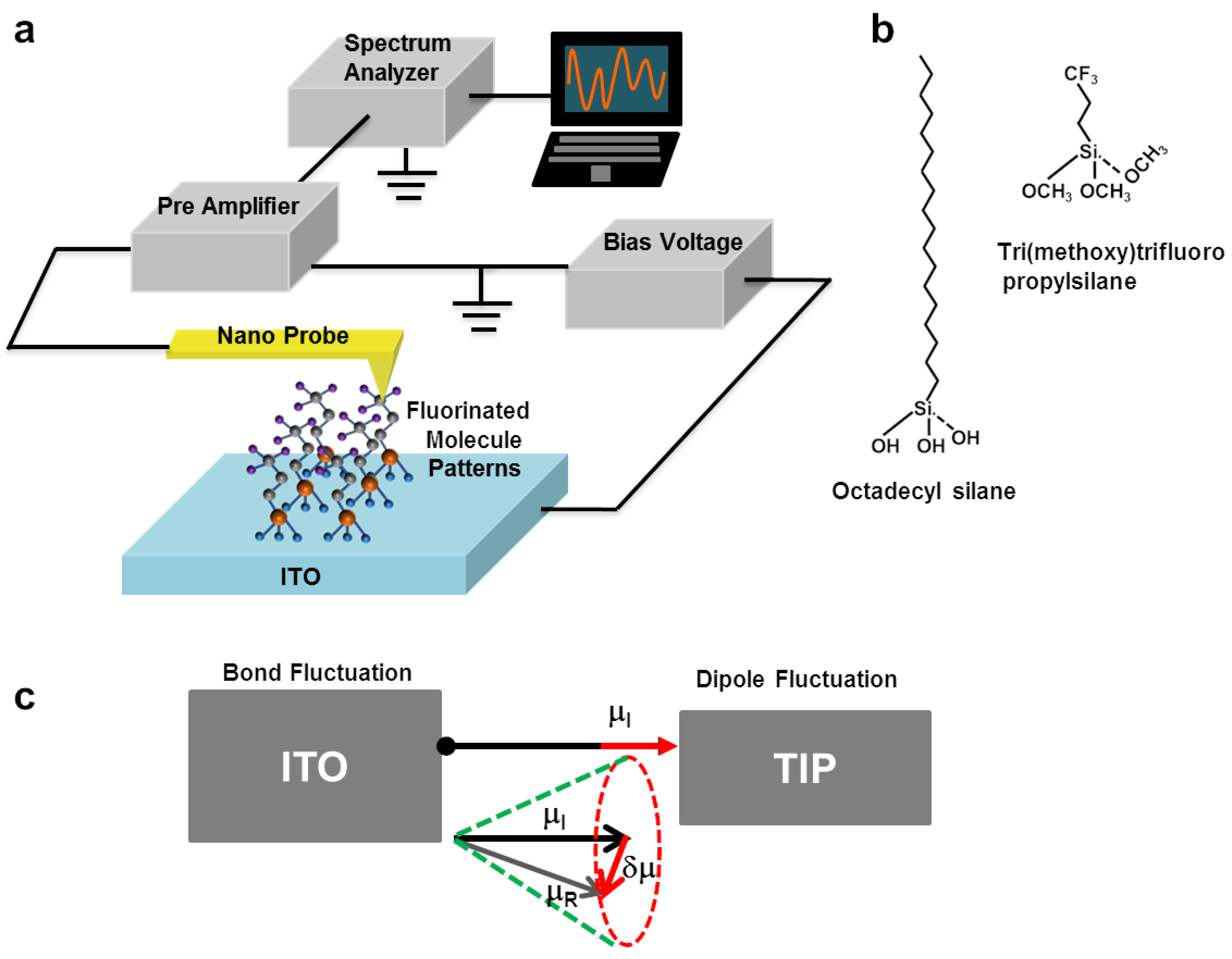
2. Materials and Methods

Trimethoxy(3,3,3-trifluoropropyl) silane (TTPS) of purity ≥97% (product id 91877) and octadecylsilane (OTS) of purity ≥90% were purchased from Sigma-Aldrich (Buchs, Switzerland). ITO substrates with a low sheet resistance (~8 Ω-□−1) and a smooth surface were also obtained from Sigma-Aldrich (Saint Louis, MO, USA) (Product ID 703192). Polydimethylsiloxane (PDMS) and curing agent of silicone elastomer were purchased from Dow Corning Corporation, Midland, MI, USA. A micro-contact printing method was utilized to pattern OTS or TTPS molecules on an ITO substrate, as reported previously [13,14]. In this process, we first cleaned the ITO substrate via oxygen plasma to minimize impurities and improve the uniformity of the substrate, as reported previously [27]. For the stamping of molecular layer patterns, a PDMS stamp was first dipped in a molecular wire solution with a concentration 10 mM in hexane for one minute. Then, the stamp was dried for 10 s under a gentle flow of N2. The inked stamp was directly placed on an ITO substrate for 5 s with a gentle pressure by the hand, so that molecules were transferred from the stamp to the ITO and formed the SAM patterns of desired molecular wires. Finally, the substrate was rinsed with ethanol to remove unbound stray molecular wires, leaving a clean patterned surface. Previous work showed that the Trimethoxy(3,3,3-trifuoropropyl)silane is one of the silanes that formed a stable monolayer without significant aggregation [28]. The unattached molecular silane could be easily removed by rinsing with the solvent. The topography and lateral force images on our molecular patterns show a rather uniform flat surface without any molecular aggregation or multilayer formation (Figure S1, Supplementary Materials), which is consistent with previously-reported results. The prepared molecular layer sample was kept under a low vacuum condition (~µbar) until the electrical measurements were carried out [29].

3. Results and Discussion

3.1. Mapping of Electrical Currents and Dipolar Noises in Patterned Self-Assembled Monolayer

Figure 1a shows a schematic illustration of the experimental setup for mapping dipole noises of a molecular wire on the ITO substrate. For noise measurements, a Pt-based conducting probe (25Pt300B, Park System, Suwon-si, Korea) installed on a conducting AFM (XE-70 model of Park System) made direct contact with a molecular wire sample and was used to measure electrical currents through the molecular wires from the ITO substrate. All measurements were performed under ambient conditions at a room temperature of ~24 °C. The contact force on the conducting probe was maintained at 1.0 μN through a feedback loop in the AFM system. It should be mentioned that the diameter of our conducting probe was ~25 nm, implying ~100 times larger tip-substrate contact area than that of the common AFM probe. Such a rather large contact area reduced the pressure by the probe, minimizing the tip-induced damage on the substrate. Furthermore, it allows us to achieve a rather stable tip-substrate junction for reliable conducting AFM mapping [25,26]. During the mapping process, a bias voltage of 0.1 V was applied to the ITO substrate using a function generator (DS345, Stanford Research Systems, Sunnyvale, CA, USA). The measured current was transformed to the amplified voltage signal by a low-noise preamplifier (SR570, Stanford Research Systems). The amplified signals were filtered by a band-pass filter (6 dB) to obtain the absolute electrical noise signal (SI), which is the fluctuating component of the current signals. The RMS power of the noise signal could be obtained using a home-made RMS-to-DC converter based on an AD737 chip (purchased from Analog Devices, Wilmington, MA, USA). Note that the obtained noise power was the integrated value of the noise PSD over the pass band of the used band-pass filter. Finally, we obtained the noise PSD value at the central frequency of the pass band by dividing the square of the measured RMS noise power with the bandwidth of the band-pass filter. By scanning the AFM probe on the patterned surface, we could simultaneously obtain the topography, current, and noise PSD maps.

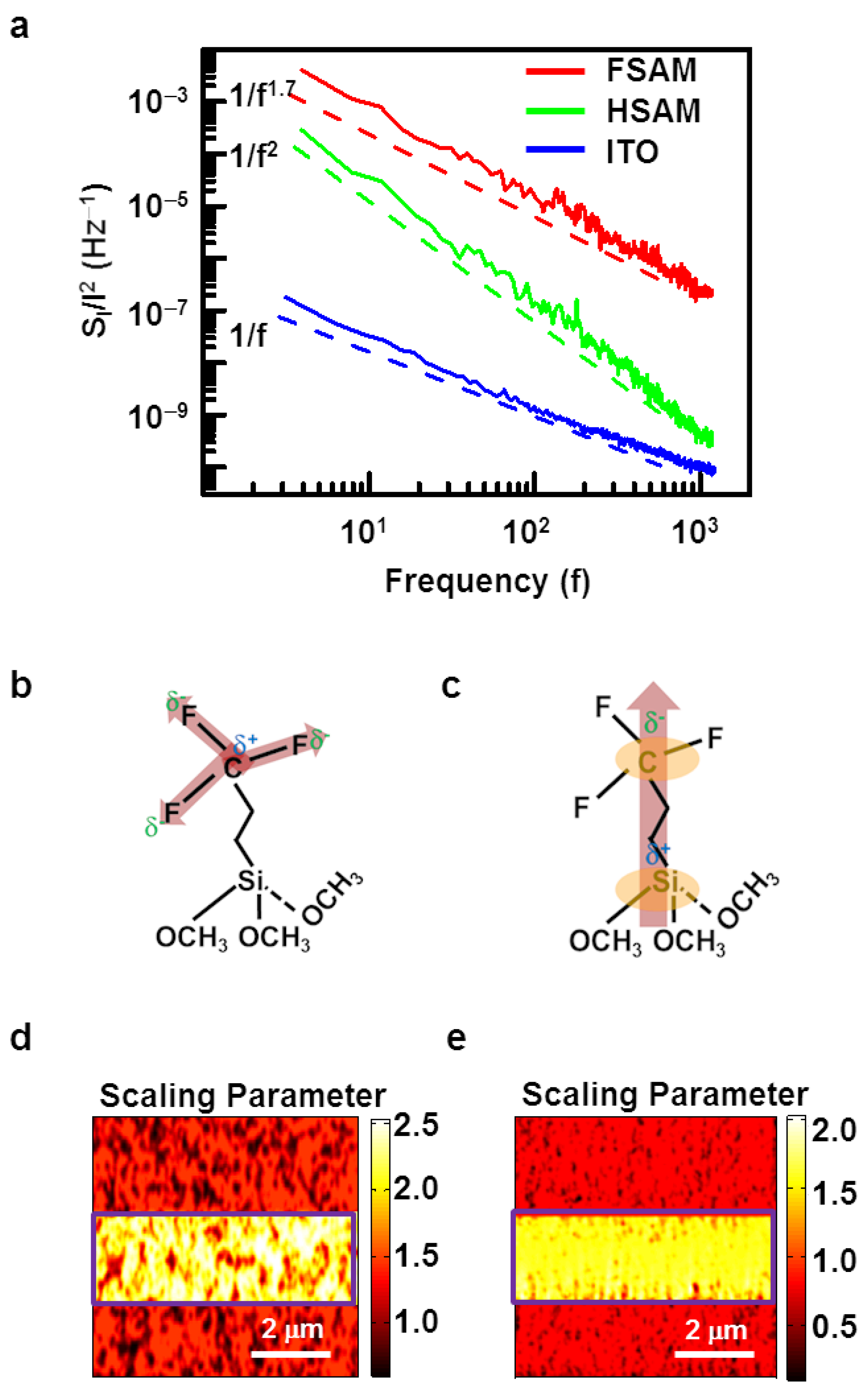
3.2. Origin of Dipolar Noises in Molecular Wires

Figure 1b shows chemical structures of octadecylsilane (OTS), and Trimethoxy(3,3,3-trifluoropropyl) silane (TTPS) molecules. OTS molecules have eighteen –CH2 units in a backbone chain, whereas TTPS molecules have only three –CH2 units in the backbone chain. The terminal group of OTS is –CH3, whereas TTPS has an electron-withdrawing terminal group of –CF3. Both molecular wires can form ordered SAM structures [18,19,20,21,22,23,24].
Figure 1c is the schematic diagram of a molecular wire junction between an ITO substrate and a conducting probe. The heads (tripod atoms) of a molecular wire could make chemi-adsorbed bonds at surface atoms of the ITO substrate [8,30]. At the other end, the coupling between the tip and the molecule (terminal) can enable electron tunneling and may alter the SAM properties in different manners such as lattice distortions, charge rearrangements, and the formation of electric dipole moments [31,32,33,34,35]. It also should be mentioned that the chemi-adsorbed bonding on the substrate may fluctuate and even migrate from one atom to another one due to various stimuli such as Joule heating and an external bias [36,37,38]. Previously, thermally activated spontaneous breakdown of the chemi-adsorbed bond has been observed on Joule heating, which could lead to migration of bonding sites of the substrate [14,36,37,38]. In the absence of a trapping-de-trapping phenomenon, the bond fluctuation is the main source of noise or resistance fluctuation in the molecular wire [4,7,14,37]. Additionally, there could be some fluctuations in electrostatic interactions between the tip and the molecular wire due to a rather high electric field by a bias voltage on the tip. Hence, electrical noises in a common molecular wire are generated by the fluctuations in bonds at the substrate and the electrostatic fluctuations at the tip-molecule junction. On the other hand, in molecular wires with rather strong dipole moments, dipole-induced fluctuations may contribute significantly to the noise [39,40,41]. In the schematic diagram, we show a vector diagram depicting a dipole moment fluctuation. The μI is the initial dipole moment of the molecular wire that changes to μR after the application of an external electric field. The δμ is the corresponding fluctuation in the dipole moment producing additional noises as δμ could affect the tunneling currents at the junction.

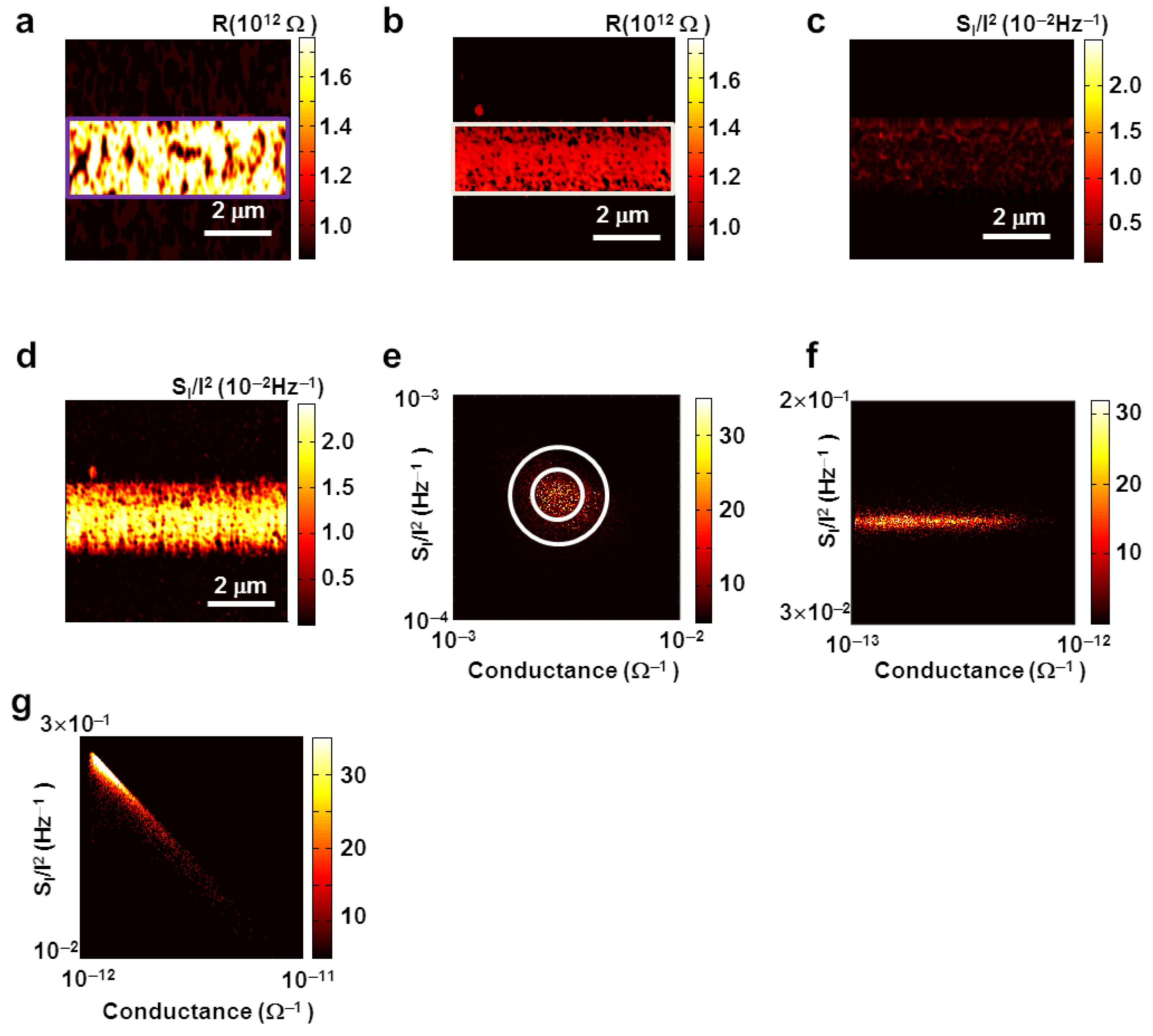
3.3. Resistance Estimation of the Individual Molecular Wire from the Current Image of SAMs

Figure 2a,b show the resistance maps of HSAM and FSAM patterns on ITO substrates, respectively. The map of averaged resistance (R) values for individual molecular wires in the SAM patterns was obtained from the corresponding current maps measured at 0.1 V. The current (I) measured through the c-AFM probe is proportional to the contact area (A) between the tip and SAM, and the packing density of the molecular wires (n) in the SAM. Hence, the R of each wire in the SAM can be estimated as R = A(nV/I), assuming the wires are parallel to each other [14]. By substituting the variables with typical values for the contact area between our tip and the SAM (close to the actual area of the probe ~2000 nm2) and the packing density of a patterned SAM on the ITO substrate (~2 nm−2) [12,13,14,15], we could obtain the resistance map of an individual molecular wire. The averaged resistance map of the HSAM pattern on the ITO substrate showed an individual molecule resistance value of ~1.6 × 10¹² Ω in the 2 μm width, which was consistent with the previously measured resistances in alkane chain molecular wires [14,15,16]. Previously, lateral force microscopy imaging has been extensively utilized to show the formation of thin SAM patterns because it is often difficult to obtain a clear contrast on topography images of such a thin molecular layer on a rather rough surface [42,43]. In our case, the lateral force images of our SAM patterns exhibited a clear contrast, confirming the formation of the SAM pattern (Supplementary Materials, Figure S1). The resistance map for the FSAM molecules shows an individual molecule resistance value of ~1.2 × 10¹² Ω, which is comparable to that of the HSAM molecular pattern, despite the fact that the length of the FSAM molecules was much shorter than that of the HSAM [16,24]. As a control experiment to analyze the substrate roughness, we also imaged a bare ITO and other substrates, showing that our ITO substrate had a flat surface comparable to that of other commonly-used substrates such as bare Au (Figures S1 and S2 in Supplementary Materials). The root-mean square (RMS) values of surface roughness for the ITO and the gold surfaces were 6 and 4 nm, respectively. It supports the notion that the resistance maps originated from molecular layer patterns on the ITO substrate. The rather large resistance in the FSAM can be explained by the fluorination of the molecules. Note that the resistance of a molecular wire of the same species increases exponentially with the length (d) of a molecular wire, following the relationship as in [14,15,16]
R   =   R 0 exp ( α d )  
where α is a tunneling attenuation factor that depends on the barrier height, and pre-factor R0 depends on junction resistances [13,14,15,16]. Previous works showed that, due to fluorine atoms, the electron cloud is skewed towards the terminal (fluorine atoms), resulting in a rather large contact resistance due to the poor coupling of the molecule with substrate and the obstruction in the charge transmission [16,24]. These effects could lead to much larger R0 and α for FSAMs than HSAMs, increasing the overall resistance of a fluorinated molecule by two or three orders of magnitudes [16,24]. For example, the resistance values of similar alkane molecules (C-8) with or without fluorine groups can differ by three orders of magnitude [15]. We chose a much smaller length of the FSAM molecule so that the resistance and noise would be comparable to those of the HSAM. Our results show that the substitution of atoms in a molecular wire can indeed significantly change the transport properties of a SAM.

3.4. Correlation between Conductance and Noise in HSAMs and FSAMs

Figure 2c,d are the maps of current normalized noise PSD (SI/I2) spectra measured on the HSAM and FSAM, respectively. Here, we mapped the noise values (SI) at a central frequency of 17.2 Hz along with the topography and current maps via the scanning noise microscopy. A current-normalized noise PSD (SI/I2) map was obtained by dividing the SI values in the SI map by the corresponding current values in the current map. The PSD of the HSAM was of the order of 5 × 10⁻³ Hz−1, whereas the FSAM exhibited an order higher PSD of ~1 × 10⁻² Hz−1. Previous works showed that longer molecular wires usually exhibit larger noises as well as larger resistance values than shorter ones [40]. However, in our case, an HSAM pattern with longer molecular length and higher R had a lower noise level than FSAM patterns. Presumably, a stronger dipole in a C–F bond could create defects and disorder in the FSAM, resulting in a higher noise level, as reported previously [23,24]. These results show that the noise PSD is very sensitive to molecular species in a SAM, and it can be utilized as a means to distinguish between different molecular wires.
Figure 2e,f are two-dimensional histogram plots showing the relationship between the noise PSDSI/I2 and the conductance on a log-log scale for bare ITO and molecular wire (HASM) coated ITO surface, respectively. The graphs were obtained by statistical weightage plotting of the conductance and noise PSD data on x and y axes, respectively. For the ITO, noise PSD amplitude SI/I2 showed some variations in terms of conductance change over the ITO surface. The variation in the noise PSD was mostly confined within two concentric circles, as marked with white lines in Figure 2e. The noise PSD and conductance variations on the surface of the ITO were small, implicating an electrically homogeneous surface [44]. Such a distribution centered in the small region of conductance and noise PSD could be attributed to the mechanical oscillations of the direct point contact between the tip and the surface atoms, as reported previously [44,45]. The data in the inner circle represent the mechanical oscillations of the atoms in direct contact with the tip, whereas the outer circle regions indicate those from neighboring atoms [44,45]. This implies that the oscillations of neighboring atoms could affect the conductance and the noise severely, and hence we can expect different conductance and noise levels depending on the materials of the tip and the surface, where the coordination numbers and packing arrangements of atoms vary from material to material. In this case, there was a direct coupling between the atoms of the ITO and the tip. Conversely, there was no direct contact between atoms of the surface and the tip in the case of HSAM, and they were connected through molecular wire (Figure 2f). Here, the noise PSD of HSAM (SI/I2) shows no significant dependence on the conductance, and noise PSD varies parallel to the conductance axis (x-axis), which is consistent with the results for typical alkane-based SAMs, as reported previously [12,46]. One can derive the noise PSD SI/I2 from the resistance fluctuation, as reported previously [14].
By differentiating the Equation (1) for a molecular wire resistance, we obtain:
SI/I2 = <δR2>/R2 = <δR02/R02> + d2α2> + α2d2>.
Here, the first term comes from the fluctuation of contact resistance between the substrate and molecules [14]. The second term represents the tunneling barrier fluctuations [4]. Here, α is related to the tunneling barrier height like α = (2meΦ)1/2/ħ, where me and Φ are an effective electron mass and a tunnel barrier height, respectively. The third term originates from the fluctuations of the molecular length d due to torsion and chain twisting [14]. Previous studies showed that in the case of alkane chain-based molecular wire layers (such as HSAM) at a low bias condition, there was not much fluctuation in the barrier height and the molecular length, and the contact resistance fluctuation (first term in Equation (2)) caused by bond fluctuations dominated its electrical noises [4,14,46]. In this case, we can consider only the first term of Equation (2), while ignoring other terms. Note that the molecule-substrate contact resistance R0 is determined by the binding of molecules on the substrate and is expected to be the same for any molecules that bind to the substrate with identical chemisorbing groups. Previous works showed that different molecular species, as long as they bound to the substrate with the same chemisorbing groups, exhibited a constant value of <δR02/R02> [14,44,45,46]. Since all HSAM molecules in the SAM bound to the substrate using the same silane groups, we can expect that <δR02/R02> should remain constant and independent of the location on the SAM. Thus, from Equation (2), we can expect almost a constant value for noise PSD SI/I2, which is consistent with our results (Figure 2f) [14,44,45,46].
Figure 2g is a two-dimensional histogram plot showing the relationship between noise PSDSI/I2 and conductance on a log-log scale for the FSAM. The noise PSD in the FSAM showed a strong negative correlation with its conductance. In this case, the noise PSD SI/I2 decreased with the increase in the conductance G, following the relationship like SI/I2G−2. Previously, such scaling behavior of the noise PSD with conductance has been explained by different electrical characteristics of the SAM [2,4,44,45,46,47]. For example, the scaling behavior and current noises in non-polar molecular wires were attributed to the characteristics of the tunneling currents and resistance fluctuations in molecular wires [44,45,46,47]. However, in the FSAM, the formation of strong dipoles could lead to a significant fluctuation in the tunneling barrier at molecular junctions [24]. This tunnel barrier fluctuation could lead to the fluctuation in the attenuation factor α. The noise due to the dipole fluctuation is relatively high because of the direct coupling with the tip, and it can exceed the noise due to the contact resistance fluctuation [48]. Previous works showed that the induced dipole in molecules could cause the dipole fluctuation with its relaxation time in the range of milli-seconds [38,39,45,46,47]. Such dipole fluctuations in individual molecules could work as a noise source to generate electrical current noises, as we observed (Figure S3, Supplementary Materials) [14]. However, it should be mentioned that the generation process of noises, in general, is a random process, and thus the dipoles of all molecules in our sample do not fluctuate simultaneously. When a dipole-induced noise is a dominant term, the noise PSD can be written as SI/I2SI-dipole/Idipole2, where Idipole is the current including the effect of electric field redistribution induced by the dipole in the molecule, and SI-dipole is the corresponding fluctuation in the current. Previous works showed that the dipole-induced noise SI-dipole is proportional to the square of the dipole moment fluctuation Δμ like SI-dipole ~ (Δμ)2 [48,49,50]. Additionally, the charge transfer rate is reported to be proportional to the square of the dipole moment, and thus Idipole should be proportional to the second power of the dipole moment like Idipole ~μ2 [49,50]. At a rather small fixed bias condition, we can assume that Δμ is much smaller than μ, and dipole fluctuations Δμ, as well as SI-dipole, are not affected by the variation of Idipole, which is also shown in our experimental data (Figure S4, Supplementary Materials). In this case, since Idipole is proportional to the conductance G, we can obtain SI-dipole/Idipole2 ∝ 1/G2, as we observed. Our results implicate that the scaling behavior of noise PSD with conductance has a different origin in each of the different species of molecules, showing the versatility of our analysis method.

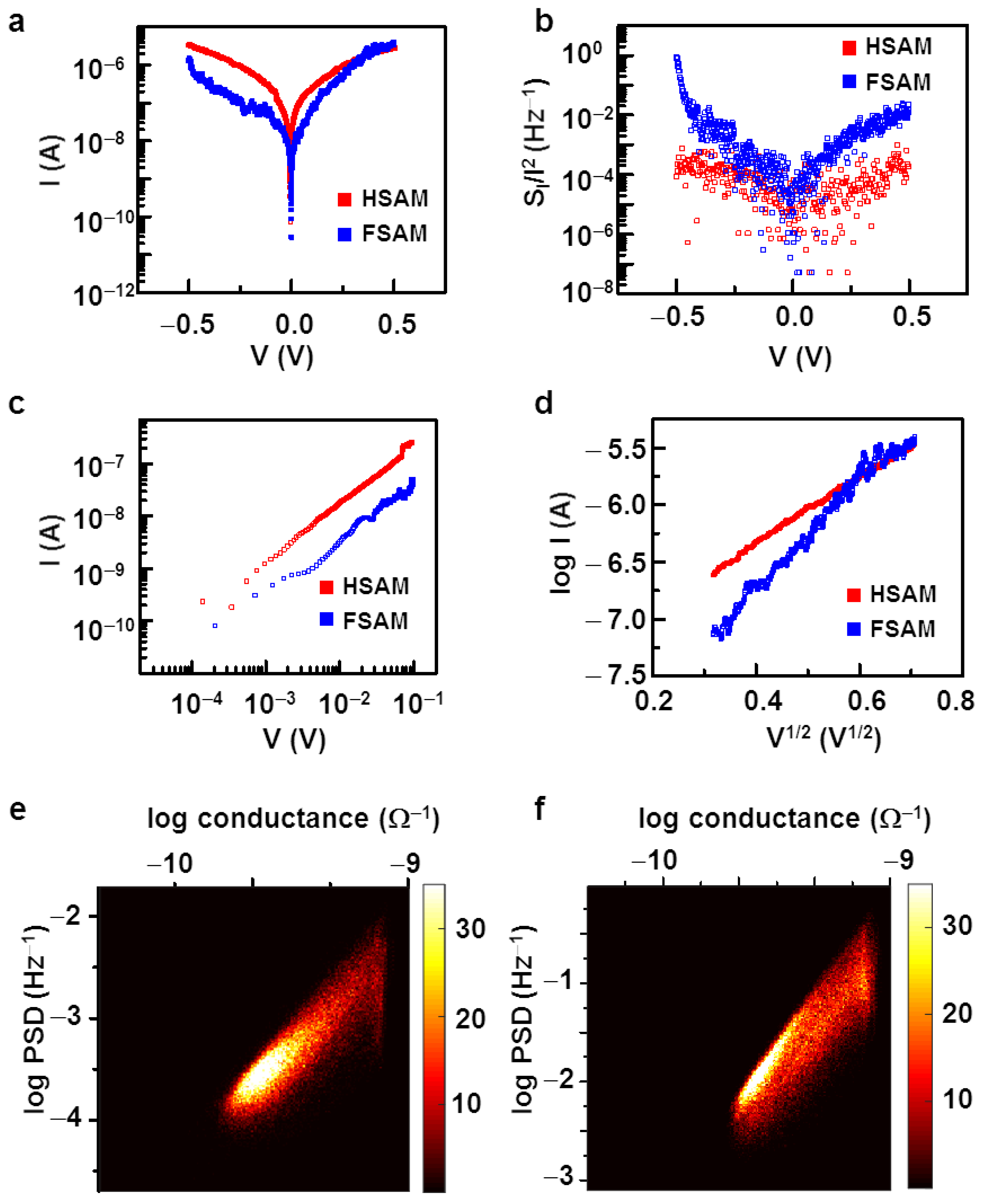
3.5. Evidence of Dipolar Interaction in FSAMs

Figure 3a shows the frequency dependence curves of normalized noise PSD (SI/I2) in the FSAM, HSAM, and ITO substrates plotted with red, green, and blue colors, respectively. The dotted lines are placed to guide the eye. The spectra were measured using a fast-Fourier transform (FFT) spectrum analyzer (SRS SR770) while keeping the conducting AFM probe stationary at a fixed location on the SAM or the ITO substrate. The overall noise PSD of SAMs was larger than ITO substrates, indicating the increased current noises at the junctions with molecular wires. Presumably, the fluctuation of bonds at molecule-ITO junctions as well as dipole moments could contribute to the increased electrical noises in SAMs. Interestingly, SAMs and ITO substrates exhibited quite different scaling behaviors. The data of the ITO substrate can be fitted by 1/f, which is typical for the system with multiple noise sources with different trapping times τ [7,51]. Previous works showed similar scaling behavior for bare Au and other conducting substrates without molecular layers [14]. On the other hand, the data on the HSAM layer can be fitted by 1/f2, which is also typical behavior for well-ordered SAM without many defects, as reported previously [14,47,51]. Previous works showed that in the junctions of molecular wires with a rather weak dipole moment such as HSAM, the bond fluctuations between molecules and substrate generate electrical noises, which can be modeled via the conductance fluctuations in two-level conducting states having the constant characteristic relaxation time τ [46,51,52]. In this case, the relaxation function φ(t) for a specific decay process can be assumed to obey a Debye relaxation, and in the time domain, the relaxation function can be expressed as φ(t) ~exp[−t/τ] [53,54,55,56]. As a result, noise PSD has a Lorentzian form like PSDτ/[1 + (2πfτ)2], and, at sufficiently high frequencies, it can be approximated as ~1/f2, which is consistent with the data of the HSAM [14,53]. However, the data of FSAM can be fitted by ~1/fβ with a rather different exponent β of ~1.7. One plausible explanation can be that the strong dipole of the FSAM could cause the fluctuation in the tunnel barrier and eventually slow down the decay process in the two-level conducting states of the noise model [50,52]. In such a case, the distribution function gets stretched on a time scale and can be modeled using the Kohlrausch–Williams–Watts (KWW) relaxation function as in [56,57].
φ(t) ~exp[−t/τ]1−γ
In principle, 1−γ could take a value between 0 and 1. In the presence of such a distribution function, the noise PSD takes the form of S(f) ~1/f2−γ [53,56,57]. For strongly disordered, heterogeneous, and interacting dielectric systems, the decay processes are very slow and γ could be as high as 0.6 [57]. In the case of FSAM, γ can be estimated as ~0.3, indicating a significant fluctuation of tunneling barriers, presumably due to the strong dipole moments of the FSAM. These results are in accordance with our assumption that the attenuation factor α (Equation (2)) is significantly affected in a FSAM.
Figure 3b,c are schematic diagrams showing the formation of dipoles in the terminal and the backbone chain of the FSAM molecular wire, respectively. Despite its rather small molecular length, the FSAM showed higher resistance and electrical noises than those of the HSAM. A plausible explanation for this is the presence of fluorine atoms on its terminal group. A fluorine atom has very high electronegativity and, thus, can form strong dipoles in an atomic bond with carbon (Figure 3b). The strength of the C–F dipole is 1.4 Debye, and that of the C–H is 0.3 Debye [20]. The large difference in the dipolar strength could have strong effects on a densely packed FSAM. A single molecular wire has three C–F dipoles, and they can interact with the intra and inter-molecular dipoles of the molecular wires. These could lead to strong dipolar interactions in the molecular wires of the FSAM, creating more substantial barrier fluctuations and larger noises than the HSAM. Additionally, the possible formation of dipoles in the backbone chain of the molecular wire (see Figure 3c) could also contribute to the noises.
Figure 3d,e show the scaling parameter map on the HSAM and FSAM, respectively. The maps of the scaling parameter of the SAMs are differentiated by rectangular boxes from the ITO part. Here, the noise PSD values were measured in the frequency range of 17.3−1732 Hz at each point of the SAM surface and utilized to estimate the scaling factors. We fitted the PSD spectra with a function of A/fβ to obtain the scaling parameter β. The PSD spectra on the molecular monolayer exhibited the scaling behavior. The HSAM exhibited a scaling factor (β) close to 2, whereas the FSAM exhibited a scaling factor of 1.7. Note that the scaling factor map shows a clear contrast between the SAM regions and the ITO regions (β ~ 1.0). We could consistently obtain the scaling parameter from different molecular wire samples in this study, supporting the notion that measured noise signals in a molecular monolayer were from the molecular parts rather than other conducting parts in the sample. These results show that the scaling parameter analysis could be utilized to discriminate between molecular species present on a nanoscale junction.

3.6. Effect of High Biases on the Transport in HSAMs and FSAMs

A high electric field in one-dimensional molecular wires can significantly affect their transport and noise characteristics. Figure 4a shows typical current-voltage (I–V) curves on a semi-log scale for the HSAM and FSAM plotted with red and blue colors, respectively. For the measurement, a bias voltage on the ITO electrode was ramped from −0.5 to 0.5 V while keeping the Pt tip as a zero bias. The HSAM showed a nearly symmetric I–V curve. On the other hand, the FSAM showed an asymmetric behavior, where the current was higher by an order in the positive ITO electrode bias cases than that of the negative bias conditions. For example, in the case of 0.5 V or −0.5 V bias on the electrode, the rectification (I(0.5 V)/I(−0.5 V)) was ~3.5. Presumably, the presence of fluorine atoms induced the formation of dipoles at terminal groups and backbone on the FSAM, resulting in the asymmetric I–V curve [58,59,60]. One explanation for the asymmetric I–V curve at a rather large bias is the rearrangement of molecular dipoles by a large external bias voltage [61]. Previous works showed that, when molecules in SAM have a permanent dipole moment, a rather large external bias from an AFM probe can affect the dipole moments and change the thickness of the SAM, resulting in a conductance change of the SAM [62]. In our case, the fluorine groups at the end of the molecules in the FSAM are known to have negative charges. When a positive bias was applied to the conducting AFM probe, the fluorine groups were attracted toward the probe (i.e., negative bias to the ITO substrate), making the FSAM thicker [20,62]. We observed three times larger current levels at a rather large positive bias than at a negative bias, while the current levels were found to be rather symmetric at a small bias. This indicates that the induced dipole moment as a large negative bias made the SAM layer thicker and decreased conductance, which is consistent with previous reports [61,62,63,64,65].
Figure 4b shows the noise PSD dependence on voltage for the HSAM and FSAM, plotted with blue and red colors, respectively. The noise PSD was measured at 17.32 Hz along with the currents, while the voltage was swept from −0.5 to 0.5 V on the ITO surface. We observed symmetric noise PSD in the HSAM, while the noise PSD in the FSAM was asymmetric, with high values at negative biases. The increased noise in the FSAM at a negative bias on the ITO substrate could be associated with the stronger effective dipole formation at an applied negative bias. Previous studies showed that a stronger dipole could lead to a more substantial fluctuation in the tunneling width and tunneling barrier, resulting in high noise levels, which is also consistent with our results [61,62,63,64,65].
Figure 4c shows the logI versus logV curves for the HSAM and FSAM at a rather low bias below 0.1 V. Note that both data can be fitted by a curve with a slope of ~1, indicating a linear dependence of a current on the bias voltage at a low bias regime. Previous works showed that at small biases, electrical currents in a molecular junction can be explained by a tunneling current with a linear dependence on V like   I V e x p [ α d ] , which is consistent with our results [66].
On the other hand, the electrical currents at a rather high bias exhibited quite different behavior. Figure 4d shows the logI versus V1/2 curves for the HSAM and FSAM at high biases (above 0.1 V) plotted with blue and red colors, respectively. In both the curves, logI showed a linear dependence on V1/2, which is consistent with previously reported results of thermionic conduction in molecular wires at a large bias voltage [66,67]. It is worth mentioning that other transport mechanisms such as tunneling and field emission can have a similar voltage dependence behavior. However, previous works showed a temperature dependence of molecular conduction, strongly supporting thermionic emission rather than other mechanisms such as tunneling or field emission, which cannot have a temperature dependence [66,67].
Figure 4e,f are the two-dimensional histogram plots showing the relationship between noise PSDSI/I2 and conductance G at 0.5 V on a log-log scale for the HSAM and FSAM, respectively. The graphs were obtained by statistical weightage plotting of the conductance and noise PSD data at 0.5 V on the x and y axes, respectively. The noise PSD showed a strong and positive correlation with conductance in both HSAM and FSAM, following scaling behavior of SI/I2G2. This dependence is opposite to the low bias scaling behavior of PSD on conductance, where we observed a negative correlation like SI/I2G2 (see Equation (2)). The positive correlation could be explained by electrical noises in the thermionic emission at a high bias. A previous report showed that, in the thermionic emission, the carriers diffuse due to thermal energy by Joule heating, and the noise due to thermal diffusion of carriers is proportional to the square of a change in temperature like SI/I2 ∝ (ΔT)2 [68]. At a molecular junction with its conductance G, the temperature change ΔT by Joule heating should be proportional to the power generated by electrical currents such as ΔTGV2. Since the bias voltage V was kept constant during the scanning, the noise PSD can be written as SI/I2G2 at a high bias condition where the thermionic noise dominates. These results show that, at a rather high bias, a thermionic fluctuation can be a dominant noise source at molecular wire junctions.

4. Conclusions

In summary, we report a strategy to directly map the effects of dipolar interactions on electrical transport and noise in the self-assembled monolayers (SAMs) of molecular wires. In this strategy, the current and noise images were measured simultaneously on molecular wire patterns by using a conducting probe. Then, the maps were analyzed to extract characteristic parameters of dipolar noises. The FSAM molecular junctions exhibited the molecular resistance comparable with the HSAM of nearly six times longer in length, which could be due to the strong dipole formations in the FSAM obstructing the charge conduction. Furthermore, in the FSAM, the normalized noise-PSD scaled as the inverse of the square of the conductance like PSDG−2, which was explained by stronger dipolar interactions affecting the tunneling barrier in the FSAM. In addition, the frequency dependence of noise PSD showed 1/f2 behavior in the HSAM, whereas the FSAM showed a deviation, exhibiting 1/f1.7 dependence that could be attributed to the strong dipole formation slowing down the tunneling process. We observed asymmetrical current and noise only in the FSAM, owing to the strong dipole formation. Interestingly, at high biases, the conduction in HSAM and FSAM molecular wires showed the transition from tunneling to thermionic transports, which was reflected in the positive correlation of the noise PSD with conductance like PSDG2. Our results provide valuable insights about dipole noise generations in molecular wires with polarization, which could be helpful in understanding the charge transports and noise properties of molecular devices. Furthermore, we can expect that this strategy may be extended to the development of new methods for the analyses of other molecular wires with versatile non-linear behaviors such as memory effects and phonons.

Supplementary Materials

The following supporting information can be downloaded at: https://www.mdpi.com/article/10.3390/nano12081371/s1, Figure S1. Atomic force microscopy images on HSAM and FSAM prepared by a microcontact printing method on ITO substrate. (a) Topography image of HSAM patterns on ITO substrate. (b) Lateral force microscopy (LFM) image on the HSAM. We can clearly see the contrast of the lateral force values in the HSAM region and the bare ITO region. (c) AFM topography image of FSAM patterns. (d) LFM image measured on the FSAM pattern showing clear contrast between the FSAM pattern and ITO. The scale bars are 1 μm; Figure S2. Atomic force microscopy topography image of 50 nm thick Au film-surface on a SiO2 substrate. The scale bar is 500 nm; Figure S3. Noise PSD of FSAM molecules as a function of time; Figure S4. Dependence of noise (S) on current (I) on FSAM. The results show that S values exhibited a rather large fluctuations, while it does not change much with different I values.

Author Contributions

Conceptualization, data curation, formal analysis, investigation, methodology, and writing—original draft, writing—review and editing, M.J. and S.S.; data curation, formal analysis, and investigation, D.C.; investigation, validation, M.Y. and J.P.; conceptualization, funding acquisition, project administration, resources, supervision, validation, writing—original draft, and writing—review and editing, S.H. All authors have read and agreed to the published version of the manuscript.

Funding

This research was supported by the National Research Foundation of Korea (NRF) funded by the Ministry of Science and ICT (MSIT) of Korea (No. 2013M3A6B2078961 and 2020R1A2B5B02002152). S.H. would like to acknowledge the support from the Ministry of Trade, Industry, and Energy (MOTIE, Korea) (No. 20012390), Samsung Electronics Co., Ltd. (No. 201209-07908-01), and the European Research Council (ERC) under the European Union’s Horizon 2020 programme (grant agreement No. 682286).

Data Availability Statement

The data presented in this study are available on request from authors.

Conflicts of Interest

The authors declare no conflict of interest.

References

  1. Emberly, E.; Kirczenow, G. Electrical Conductance of Molecular Wires. Nanotechnology 1999, 10, 285–289. [Google Scholar] [CrossRef]
  2. Li, C.; Numata, M.; Bae, A.-H.; Sakurai, K.; Shinkai, S. Self-Assembly of Supramolecular Chiral Insulated Molecular Wire. J. Am. Chem. Soc. 2005, 127, 4548–4549. [Google Scholar] [CrossRef] [PubMed]
  3. Cui, K.; Mali, K.S.; Wu, D.; Feng, X.; Mullen, K.; Walter, M.; Feyter, S.D.; Merten, S.F.L. Ambient Bistable Single Dipole Switching in a Molecular Monolayer. Angew. Chem. Int. Ed. 2020, 59, 14049–14053. [Google Scholar] [CrossRef] [PubMed]
  4. Xiang, D.; Wang, X.; Jia, C.; Lee, T.; Guo, X. Molecular-Scale Electronics: From Concept to Function. Chem. Rev. 2016, 116, 4318–4440. [Google Scholar] [CrossRef] [PubMed]
  5. Garner, M.H.; Li, H.; Chen, Y.; Su, T.A.; Shangguan, Z.; Paley, D.W.; Liu, T.; Ng, F.; Li, H.; Xiao, S.; et al. Comprehensive Suppression of Single-Molecule Conductance Using Destructive σ-Interference. Nature 2018, 558, 415–419. [Google Scholar] [CrossRef]
  6. Celestin, M.; Krishnan, S.; Bhansali, V.; Stefankos, E.; Goswami, D.Y. A Review of Self-Assembled Monolayers as Potential Terahertz Frequency Tunnel Diodes. Nano Res. 2014, 7, 589–625. [Google Scholar] [CrossRef]
  7. Cho, D.; Shekhar, S.; Lee, H.; Hong, S. Nanoscale Mapping of Molecular Vibrational Modes via Vibrational Noise Spectroscopy. Nano Lett. 2018, 18, 1001–1009. [Google Scholar] [CrossRef]
  8. Bu, D.; Riechers, S.; Liang, J.; Liu, G.-Y. Impact of Nanografting on the Local Structure of Ternary Self-Assembled Monolayers. Nano Res. 2015, 8, 2102–2114. [Google Scholar] [CrossRef]
  9. Kim, G.-H.; de Arquer, F.P.G.; Yoon, Y.J.; Lan, X.; Liu, M.; Voznyy, O.; Yang, Z.; Fan, F.; Ip, A.H.; Kanjanaboos, P.; et al. High-Efficiency Colloidal Quantum Dot Photovoltaics via Robust Self-Assembled Monolayers. Nano Lett. 2015, 15, 7691–7696. [Google Scholar] [CrossRef]
  10. Hanson, E.L.; Guo, J.; Koch, N.; Schwartz, J.; Bernasek, S.L. Advanced Surface Modification of Indium Tin Oxide for Improved Charge Injection in Organic devices. J. Am. Chem. Soc. 2005, 28, 10058–10062. [Google Scholar] [CrossRef]
  11. Shekhar, S.; Park, I.; Kim, J.; Yang, M.; Cho, D.; Hong, S. Nanoscale Mapping of Wavelength-Selective Photovoltaic Responses in H- and J-Aggregates of Azo Dye-based Solar Cell Films. J. Mater. Chem. A 2021, 9, 632–641. [Google Scholar] [CrossRef]
  12. Koide, Y.; Such, M.W.; Basu, R.; Evmenenko, G.; Cui, J.; Dutta, P.; Hersam, M.C.; Marks, T.J. Hot Microcontact Printing for Patterning ITO Surfaces. Methodology, Morphology, Microstructure, and OLED Charge Injection Barrier Imaging. Langmuir 2003, 19, 86–93. [Google Scholar] [CrossRef]
  13. Yan, C.; Zharnikov, M.; Golzhauser, A.; Grunze, M. Preparation and Characterization of Self-Assembled Monolayers on Indium Tin Oxide. Langmuir 2000, 16, 6208–6215. [Google Scholar] [CrossRef]
  14. Cho, D.; Lee, H.; Shekhar, S.; Yang, M.; Park, J.Y.; Hong, S. Direct Mapping of Electrical Noise Sources in Molecular Wire-based Devices. Sci. Rep. 2017, 7, 43411. [Google Scholar] [CrossRef] [Green Version]
  15. Taherinia, D.; Smith, C.E.; Ghosh, S.; Odoh, S.O.; Balhorn, L.; Gagliradi, L.; Cramer, C.J.; Frisbie, C.D. Charge Transport in 4 nm Molecular Wires with Interrupted Conjugation: Combined Experimental and Computational Evidence for Thermally Assisted Polaron Tunneling. ACS Nano 2016, 10, 4372–4383. [Google Scholar] [CrossRef]
  16. Kaun, C.-C.; Guo, H. Resistance of Alkanethiol Molecular Wires. Nano. Lett. 2003, 11, 1521–1525. [Google Scholar] [CrossRef]
  17. Wold, D.J.; Haag, R.; Rampi, M.A.; Frisbie, C.D. Distance Dependence of Electron Tunneling Through Self-Assembled Monolayers Measured by Conducting Probe Atomic Force Microscopy:  Unsaturated Versus Saturated Molecular Junctions. J. Phys. Chem. B 2002, 106, 2813–2816. [Google Scholar] [CrossRef]
  18. Lee, H.J.; Jamison, A.C.; Lee, T.R. Surface Dipoles: A Growing Body of Evidence Supports Their Impact and Importance. Acc. Chem. Res. 2015, 48, 3007–3015. [Google Scholar] [CrossRef]
  19. Zenasni, O.; Marquez, M.D.; Jamison, A.C.; Lee, H.J.; Czader, A.; Lee, T.R. Inverted Surface Dipoles in Fluorinated Self-Assembled Monolayers. Chem. Mater. 2015, 27, 7433–7446. [Google Scholar] [CrossRef]
  20. Liao, K.-C.; Bowers, C.M.; Hyo, J.Y.; Whitesides, G.M. Fluorination and Tunneling Across Molecular Junctions. J. Am. Chem. Soc. 2015, 137, 3852–3858. [Google Scholar] [CrossRef] [Green Version]
  21. Zenasni, O.; Jamison, A.C.; Lee, T.R. The Impact of Fluorination on the Structure and Properties of Self-Assembled Monolayer Films. Soft Mater. 2013, 9, 6356–6370. [Google Scholar] [CrossRef]
  22. Pujari, S.P.; van Andel, E.; Yaffe, O.; Cahen, D.; Weidner, T.; van Rijn, C.J.M.; Zuilhof, H. Mono-Fluorinated Alkyne-Derived SAMs on Oxide-Free Si(111) Surfaces: Preparation, Characterization and Tuning of the Si Workfunction. Langmuir 2013, 29, 570–580. [Google Scholar] [CrossRef] [PubMed]
  23. Osella, S.; Cornil, D.; Cornil, J. Work Function Modification of the (111) Gold Surface Covered by Long Alkanethiol-Based Self-Assembled Monolayers. Phys. Chem. Chem. Phys. 2014, 16, 2866–2873. [Google Scholar] [CrossRef] [PubMed]
  24. Pflaum, J.; Bracco, G.; Schreiber, F.; Colorado, R., Jr.; Shmakova, O.E.; Lee, T.R.; Scoles, G.; Kahn, A. Structure and Electronic Properties of CH3- and CF3- Terminated Alkanethiol Monolayers on Au(111): A Scanning Tunneling Microscopy, Surface X-ray and Helium Scattering Study. Surf. Sci. 2002, 498, 89–104. [Google Scholar] [CrossRef]
  25. Yang, G.; Amro, N.A.; Liu, G.-Y. Scanning Probe Lithography of Self-Assembled Monolayers. Proc. Nanofabr. Tech. SPIE 2003, 5220, 52–65. [Google Scholar]
  26. Ishida, T.; Mizutani, W.; Akiba, U.; Umemura, K.; Inoue, A.; Choi, N.; Fujihira, M.; Tokumoto, H. Lateral Electrical Conduction in Organic Monolayer. J. Phys. Chem. B 1999, 103, 1686–1690. [Google Scholar] [CrossRef]
  27. Jeon, H.; Kim, J.; Shekhar, S.; Park, J.; Hong, S. Mapping the Nanoscale Effects of Charge Traps on Electrical Transport in Grain Structures of Indium Tin Oxide Thin Films. Nanoscale Adv. 2021, 3, 5008–5015. [Google Scholar] [CrossRef]
  28. Einati, H.; Mottel, A.; Inberg, A.; Shacham-Diamond, Y. Electrochemical Studies of Self-Assembled Monolayers Using Impedance Spectroscopy. Electrochim. Acta 2009, 54, 6063–6069. [Google Scholar] [CrossRef]
  29. Long, D.P.; Lazorcik, J.L.; Mantooth, B.A.; Moore, M.H.; Ratner, M.A.; Troisi, A.; Yao, Y.; Ciszek, J.W.; Tour, J.M.; Shashidhar, R. Effects of Hydration on Molecular Junction Transport. Nat. Mater. 2006, 5, 901–908. [Google Scholar] [CrossRef]
  30. Hakkinen, H. The Gold–Sulfur Interface at the Nanoscale. Nat. Chem. 2012, 4, 443–455. [Google Scholar] [CrossRef]
  31. Blackman, G.S.; Mate, C.M.; Philpott, M.R. Interaction Forces of a Sharp Tungsten Tip with Molecular Films on Silicon Surfaces. Phys. Rev. Lett. 1990, 65, 2270–2273. [Google Scholar] [CrossRef] [PubMed]
  32. Ciraci, S.; Baratoff, A.; Batra, I.P. Tip-Sample Interaction Effects in Scanning-Tunneling and Atomic-Force Microscopy. Phys. Rev. B 1990, 41, 2763–2775. [Google Scholar] [CrossRef] [PubMed]
  33. Caffrey, N.-M.; Buchmann, K.; Haupmann, N.; Ferriani, V.; Heinze, S.; Berndt, R. Competing forces during contact formation between a tip and a single molecule. Nano Lett. 2015, 15, 5156–5160. [Google Scholar] [CrossRef] [PubMed]
  34. Datta, S.; Tian, W.; Hong, S.; Reifenberger, R.; Henderson, J.I.; Kubiak, C.P. Current-Voltage Characteristics of Self-Assembled Monolayers by Scanning Tunneling Microscopy. Phys. Rev. Lett. 1997, 79, 2530–2533. [Google Scholar] [CrossRef]
  35. Xue, Y.; Datta, S.; Hong, S.; Reifenberger, R.; Henderson, J.I.; Kubiak, C.P. Negative Differential Resistance in the Scanning-Tunneling Spectroscopy of Organic Molecules. Phys. Rev. B 1999, 59, R7852–R7855. [Google Scholar] [CrossRef] [Green Version]
  36. Huang, Z.; Chen, F.; Bennett, P.A.; Tao, N. Single Molecule Junctions Formed via Au-Thiol Contact: Stability and Breakdown Mechanism. J. Am. Chem. Soc. 2007, 129, 13225–13231. [Google Scholar] [CrossRef]
  37. Ramachandran, G.K.; Hopson, T.J.; Rawlett, A.M.; Nagahara, L.A.; Primak, A.; Lindsay, S.M. A Bond-fluctuation Mechanism for Stochastic Switching in Wired Molecules. Science 2003, 300, 1413–1416. [Google Scholar] [CrossRef]
  38. Zang, Y.; Fung, E.-D.; Fu, T.; Ray, S.; Garner, M.H.; Borges, A.; Steigerwald, M.L.; Patil, S.; Solomon, G.; Venkatraman, L. Voltage-Induced Single-Molecule Junction Planarization. Nano Lett. 2021, 21, 673–679. [Google Scholar] [CrossRef]
  39. Pleutin, S.; Clement, N.; Guerin, D.; Vuillaume, D. Molecular Relaxation Dynamics in Organic Monolayer Junctions. Phys. Rev. B 2010, 82, 125436. [Google Scholar] [CrossRef]
  40. Clement, N.; Pleutin, S.; Seitz, O.; Lenfant, S.; Vuillaume, D. 1/fγ Tunnel Current Noise Through Si-bound Alkyl Monolayers. Phys. Rev. B 2007, 76, 205407. [Google Scholar] [CrossRef] [Green Version]
  41. Handziuk, V.; Gasparyan, F.; Vandamme, L.K.J.; Coppola, M.; Sydoruk, V.; Petrychuk, M.; Mayer, D.; Vitusevich, S. Noise Spectroscopy of Tunable Nanoconstrictions: Molecule-Free and Molecule-Modified. Nanotechnology 2018, 29, 385704. [Google Scholar] [CrossRef] [PubMed] [Green Version]
  42. Hong, S.; Zhu, J.; Mirkin, C.A. Multiple Ink Nanolithography: Toward a Multiple-Pen Nano-Plotter. Science 1999, 286, 523–525. [Google Scholar] [CrossRef] [PubMed]
  43. Hong, S.; Mirkin, C.A. A Nanoplotter with Both Parallel and Serial Writing Capabilities. Science 2000, 288, 1808–1811. [Google Scholar] [CrossRef] [PubMed] [Green Version]
  44. Adak, O.; Rosenthal, E.; Meisner, J.; Andrade, E.F.; Pasupathy, A.N.; Nuckolls, C.; Hybertsen, M.S.; Venkatraman, L. Flicker Noise as a Probe of Electronic Interaction at Metal–Single Molecule Interfaces. Nano Lett. 2015, 15, 4143–4149. [Google Scholar] [CrossRef] [PubMed]
  45. Venkataraman, L.; Klare, J.E.; Tam, I.W.; Nuckolls, C.; Hybertsen, M.S.; Steigerwald, M.L. Single-Molecule Circuits with Well-Defined Molecular Conductance. Nano Lett. 2006, 6, 458–462. [Google Scholar] [CrossRef] [PubMed] [Green Version]
  46. Cho, D.; Yang, M.; Shin, N.; Hong, S. Mapping Reversible Photoswitching of Molecular Resistance Fluctuations During the Conformational Transformation of Azobenzene-Terminated Molecular Switches. Nanotechnology 2018, 29, 365705. [Google Scholar] [CrossRef]
  47. Sydoruk, V.A.; Xiang, D.; Vitusevich, S.A.; Petrychuk, M.V.; Vladyka, A.; Zhang, Y.; Offenhausser, A.; Kochelap, V.A.; Belyaev, A.E.; Mayer, D. Noise and Transport Characterization of Single Molecular Break Junctions with Individual Molecule. J. Appl. Phys. 2012, 112, 014908. [Google Scholar] [CrossRef] [Green Version]
  48. Dubessy, R.; Coudreau, T.; Guidoni, L. Electric Field Noise above Surfaces: A Model for Heating-Rate Scaling Law in Ion Traps. Phys. Rev. A 2009, 80, 031402R. [Google Scholar] [CrossRef] [Green Version]
  49. Nalbach, P.; Puglies, I.; Langhals, H.; Thorwart, M. Noise-Induced Förster Resonant Energy Transfer Between Orthogonal Dipoles in Photoexcited Molecules. Phys. Rev. Lett. 2012, 108, 218302. [Google Scholar] [CrossRef]
  50. Safavi-Naini, A.; Rab, P.; Weck, P.F.; Sadeghpour, H.R. Microscopic Model of Electric-Field-Noise Heating in Ion Traps. Phys. Rev. A 2011, 84, 023412. [Google Scholar] [CrossRef]
  51. Ochs, R.; Secker, D.; Elbing, M.; Mayor, M.; Weber, H.B. Fast Temporal Fluctuations in Single-Molecule Junctions. Faraday Discuss. 2006, 131, 281–289. [Google Scholar] [CrossRef] [PubMed]
  52. Kim, Y.; Song, H.; Kim, D.; Lee, T.; Jeong, H. Noise Characteristics of Charge Tunneling via Localized States in Metal−Molecule−Metal Junctions. ACS Nano 2010, 4, 4426–4430. [Google Scholar] [CrossRef] [PubMed]
  53. Careri, G.; Consolini, G. Dielectric 1/f Noise of Proton Glass on a Hydrated Protein Surface. Phys. Rev. E 2000, 62, 4454–4456. [Google Scholar] [CrossRef] [PubMed]
  54. Raychaudhury, A.K. Measurement of 1/f Noise and Its Application in Materials Science. Current Opinion Soli. State Mater. Sci. 2002, 6, 67–85. [Google Scholar] [CrossRef]
  55. Bogdanovitch, S.; Popovic, D. Onset of Glassy Dynamics in a Two-Dimensional Electron System in Silicon. Phys. Rev. Lett. 2002, 88, 236401. [Google Scholar] [CrossRef] [Green Version]
  56. Russell, E.V.; Israeloff, N.E. Direct Observation of Molecular Cooperativity Near the Glass Transition. Nature 2000, 408, 695–698. [Google Scholar] [CrossRef]
  57. Alvarez, F.; Alegria, A.; Colmenaro, J. Relationship Between the Time-Domain Kohlrausch-Williams-Watts and Frequency-Domain Havriliak-Negami Relaxation Functions. Phys. Rev. B 1991, 44, 7306–7312. [Google Scholar] [CrossRef]
  58. Youssef, M.B.; Lang, P.; Seydou, M.; Kouki, F. Dipolar Self-Assembled Monolayers Grafted on ZnO for the Tuning of Electronic Properties of the Poly (3-Hexylthiophène)-[6,6]-Phenyl C61-Butyric Acid Methylester Blend. Thin Solid Film. 2020, 714, 138296. [Google Scholar] [CrossRef]
  59. Ng, M.-K.; Lee, D.C.; Yu, L. Molecular Diodes Based on Conjugated Diblock Co-oligomers. J. Am. Chem. Soc. 2002, 124, 11862–11863. [Google Scholar] [CrossRef]
  60. Chabinyc, M.L.; Chen, X.; Holmlin, R.E.; Jacobs, H.; Skulason, H.; Frisbie, C.D.; Mujica, V.; Ratner, M.A.; Rampi, M.A.; Whitesides, G.M. Molecular Rectification in a Metal−Insulator−Metal Junction Based on Self-Assembled Monolayers. J. Am. Chem. Soc. 2002, 124, 11730–11736. [Google Scholar] [CrossRef] [Green Version]
  61. Pulka-Ziach, K.; Puszko, A.K.; Juhaniewicz-Debinska, J.; Sek, S. Electron Transport and a Rectifying Effect of Oligourea Foldamer Films Entrapped Within Nanoscale Junctions. J. Phys. Chem. C 2019, 123, 1136–1141. [Google Scholar] [CrossRef]
  62. Pawlowski, J.; Juhaniewicz, J.; Tymecka, D.; Sek, S. Electron Transfer Across α-Helical Peptide Monolayers: Importance of Interchain Coupling. Langmuir 2012, 50, 17287–17294. [Google Scholar] [CrossRef] [PubMed]
  63. Takai, K.; Onuki, A. Fluctuations of Local Electric Field and Dipole Moments in Water between Metal Walls. J. Chem. Phys. 2015, 143, 154503. [Google Scholar] [CrossRef] [PubMed] [Green Version]
  64. Kambe, T.; Oshima, K. Dynamically Fluctuating Electric Dipole Moments in Fullerene-based Magnets. Sci. Rep. 2014, 4, 6419. [Google Scholar] [CrossRef] [PubMed] [Green Version]
  65. Stroscio, J.A.; Eigler, D.M. Atomic and Molecular Manipulation with the Scanning Tunneling Microscope. Science 1991, 254, 1319–1326. [Google Scholar] [CrossRef] [Green Version]
  66. Wang, W.; Lee, T.; Reed, M.A. Mechanism of Electron Conduction in Self-Assembled Alkanethiol Monolayer Devices. Phys. Rev. B 2003, 68, 035416. [Google Scholar] [CrossRef]
  67. Simmons, J.G. Generalized Formula for the Electric Tunnel Effect between Similar Electrodes Separated by a Thin Insulating Film. J. App. Phys. 1963, 34, 1793–1803. [Google Scholar] [CrossRef] [Green Version]
  68. Clarke, J.; Voss, R.F. 1/f noise from Thermal Fluctuations in Metal Films. Phys. Rev. Lett. 1974, 33, 24–27. [Google Scholar] [CrossRef]
Figure 1. Schematic diagrams showing the scanning noise measurement setup and chemical structures of molecular wires. (a) Schematic diagram depicting noise and current measurement setup for a molecular wire pattern. A dc bias was applied to the ITO substrate, and currents and noise signals through the probe were measured by a homemade network analyzer. (b) Chemical structures of octadecyl(trihydroxy)silane and tri(methoxy)trifluoropropylsilane molecular wires, which were used to pattern hydrogenated-SAM and fluorinated-SAM, respectively. (c) Schematic diagram showing the possible formation of a dipole at the tip. δμ is the change in a dipole moment due to a change in a molecular confirmation or change in position of contact atoms.
Nanomaterials 12 01371 g001
Figure 2. Resistance and noise mapping and their inter-dependence in HSAM and FSAM molecular wire patterns. (a) An individual molecular wire resistance map for a HSAM pattern (bright area). The dark area represents bare ITO surface. The order of resistance values on the HSAM regions was of ~TΩ. (b) An individual molecular wire resistance map for a FSAM pattern (bright regions) showing ~TΩ of resistance. (c) A noise PSD map for HSAM (bright regions). The order of the noise was 10−2 Hz−1. (d) A noise PSD map for FSAM (bright regions) showing a rather large noise with an order of 10−1 Hz−1. (e) A double histogram plot for noise PSD versus conductance on a log-log scale for the ITO. The concentric circular data indicate the typical behavior of a metallic point contact at the junction of the tip and ITO surface. (f) A double histogram plot for noise PSD versus conductance on a log-log scale for HSAM. The plot shows that noise PSD was nearly independent of the conductance. This is typical behavior for alkane-chain-based non-polar molecular junctions. (g) A double histogram plot for noise PSD versus conductance on a log-log scale for FSAM. Noise PSD scaled as ~G−2 implies a tunneling barrier fluctuation.
Nanomaterials 12 01371 g002
Figure 3. The frequency dependence of noise PSD and its scaling behavior in HSAM and FSAM. (a) Noise PSD as a function of frequencies in HSAM, FSAM, and ITO. HSAM exhibited 1/f2 behavior supposedly due to bond fluctuations. FSAM showed a weaker dependence like PSD ~1/f1.7, which can be attributed to the effect of dipole fluctuations. The ITO shows typical 1/f behavior commonly observed on a bulk film. (b) A schematic diagram of the bond polarization of FSAM molecule. Due to high electronegativity of fluorine, bonds are strongly polarized. (c) A schematic diagram showing backbone polarization of the FSAM. (d) A scaling parameter map of noise PSD spectra measured on HSAM (bright regions). HSAM showed a scaling parameter of 2. (e) A scaling parameter map of noise PSD spectra measured on FSAM (bright regions). FSAM regions showed scaling parameter of 1.7.
Nanomaterials 12 01371 g003
Figure 4. The effect of high biases on the conduction mechanism and noises in molecular wire junctions. (a) A scatter plot showing I–V curves of HSAM and FSAM on a semi-log scale. The curve was nearly symmetric for HSAM, whereas FSAM showed asymmetry and higher currents in positive bias cases. (b) Noise PSD dependence on the voltage for HSAM and FSAM. The noise PSD shows an asymmetric behavior in FSAM. (c) The I–V curves of HSAM and FSAM for low biases (below 0.1 V) on a log-log scale, showing the linear dependence of the current on voltage. (d) logI–V1/2 curves of HSAM and FSAM for high biases (above 0.1 V). The linear dependence of the curves implicates thermionic emission of carriers at high biases. (e) A double histogram plot for noise PSD versus conductance for HSAM at a high bias, showing a positive correlation. (f) A double histogram plot for noise PSD versus conductance for FSAM at a high bias. The positive correlations in high bias conditions implicate a change in the conduction mechanism from tunneling to thermionic emission.
Nanomaterials 12 01371 g004
Publisher’s Note: MDPI stays neutral with regard to jurisdictional claims in published maps and institutional affiliations.

