
Imaging Thermoelectric Properties at the Nanoscale

 , , and
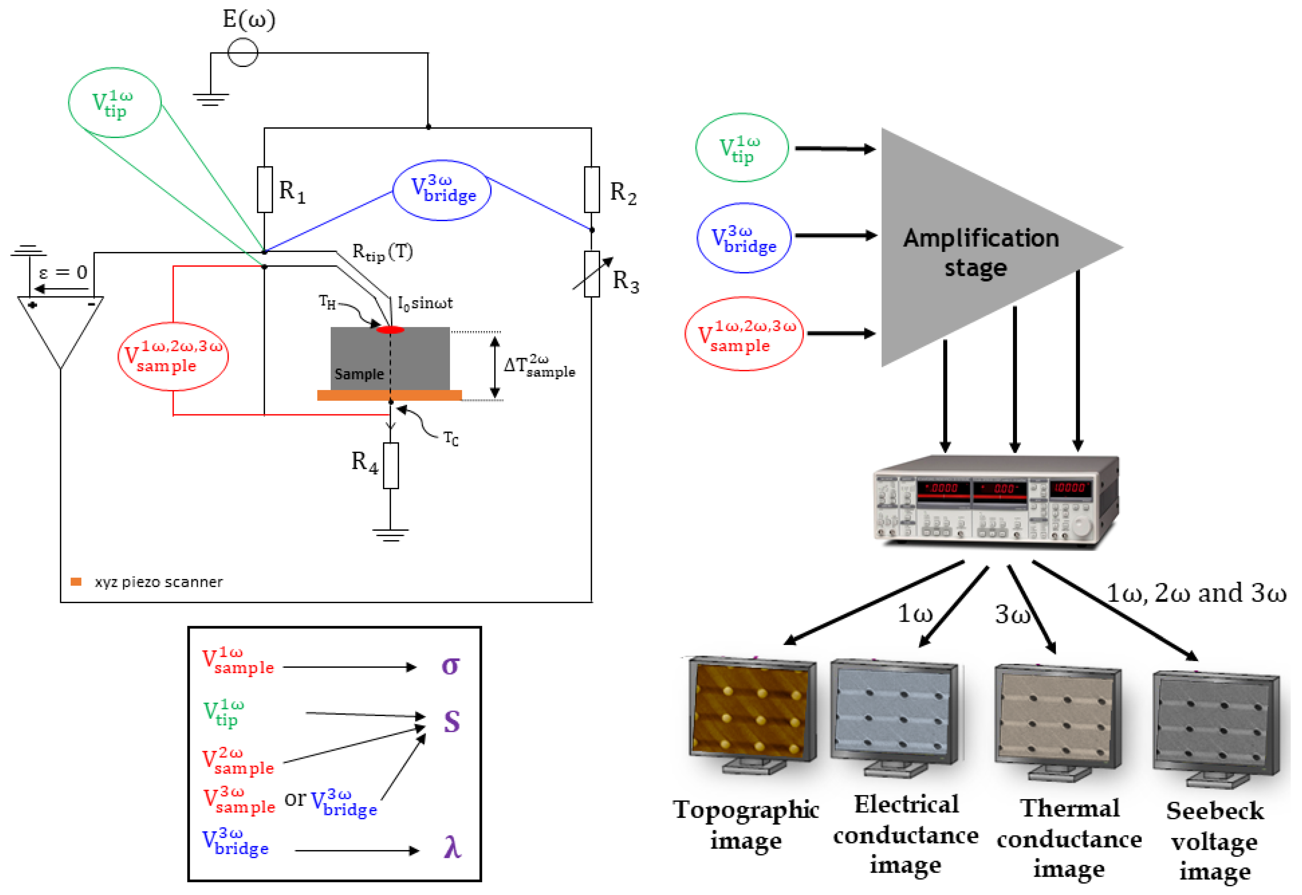
Abstract
1. Introduction
2. Materials and Methods
3. Results and Discussion
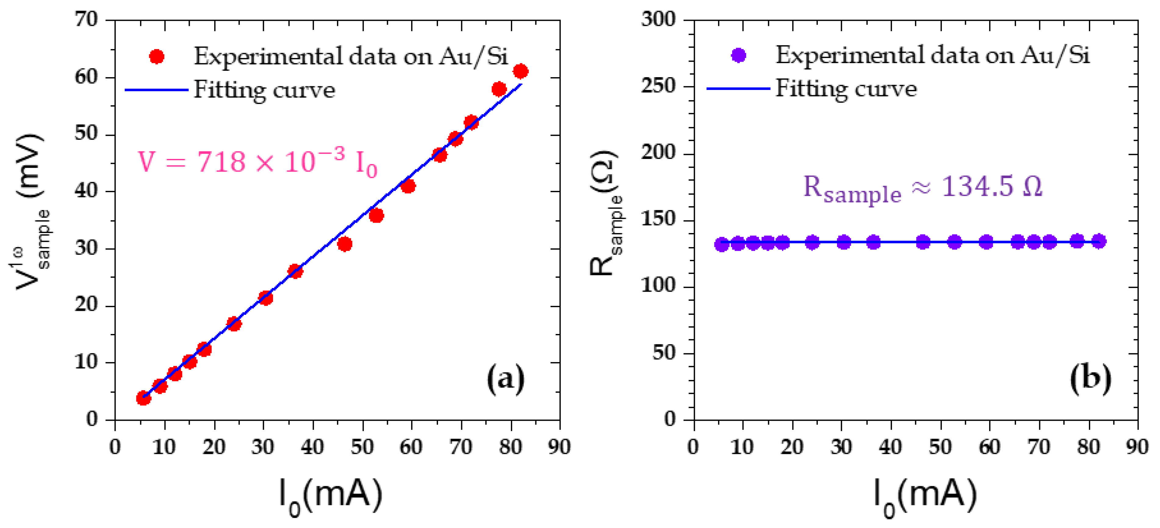
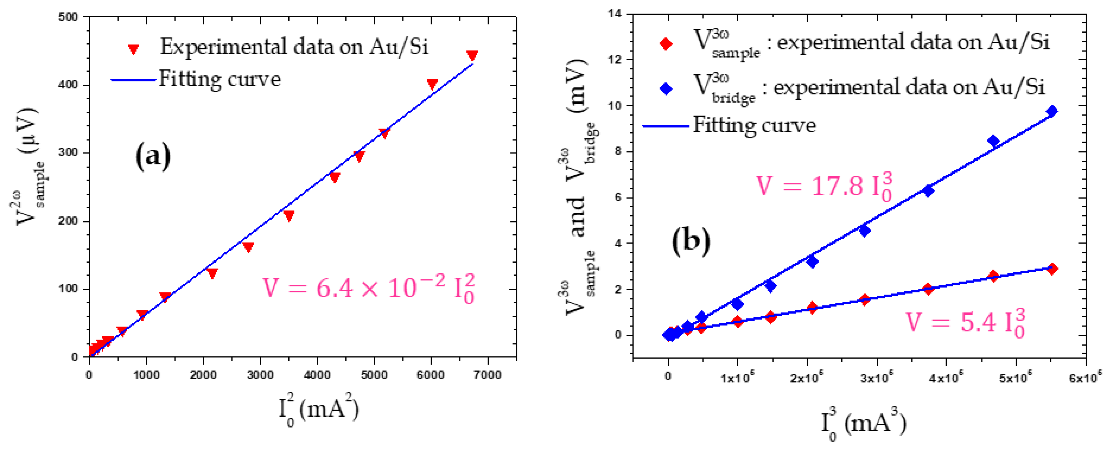
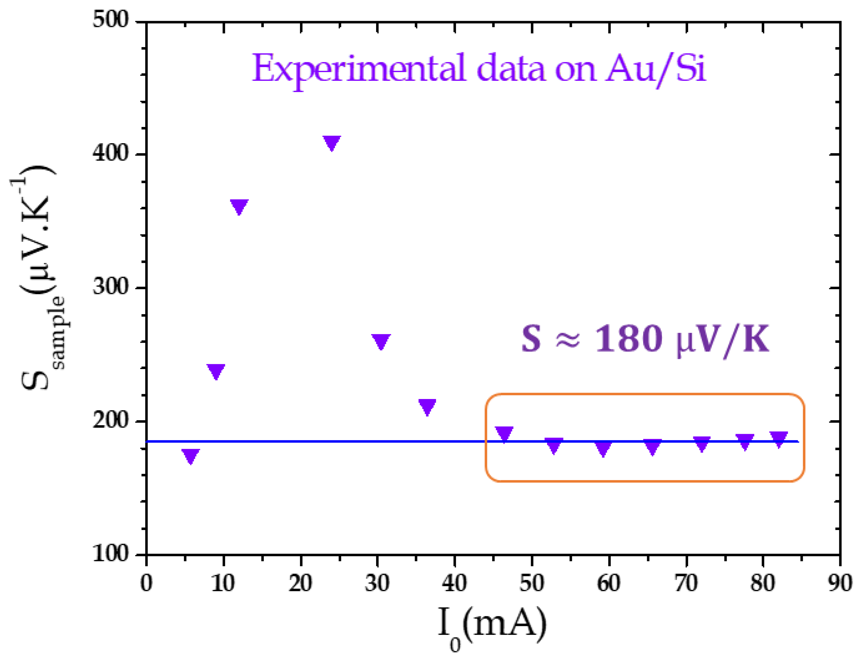
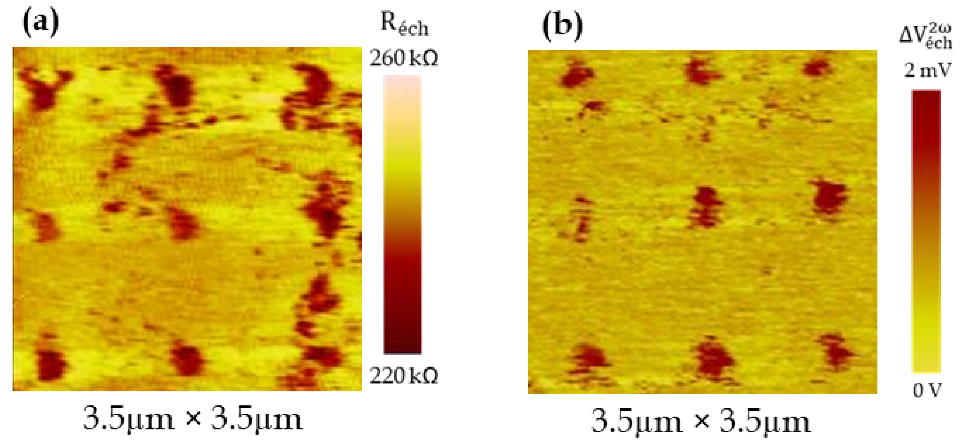
3.1. Experimental Validation on a Gold Layer/Si Substrate Sample
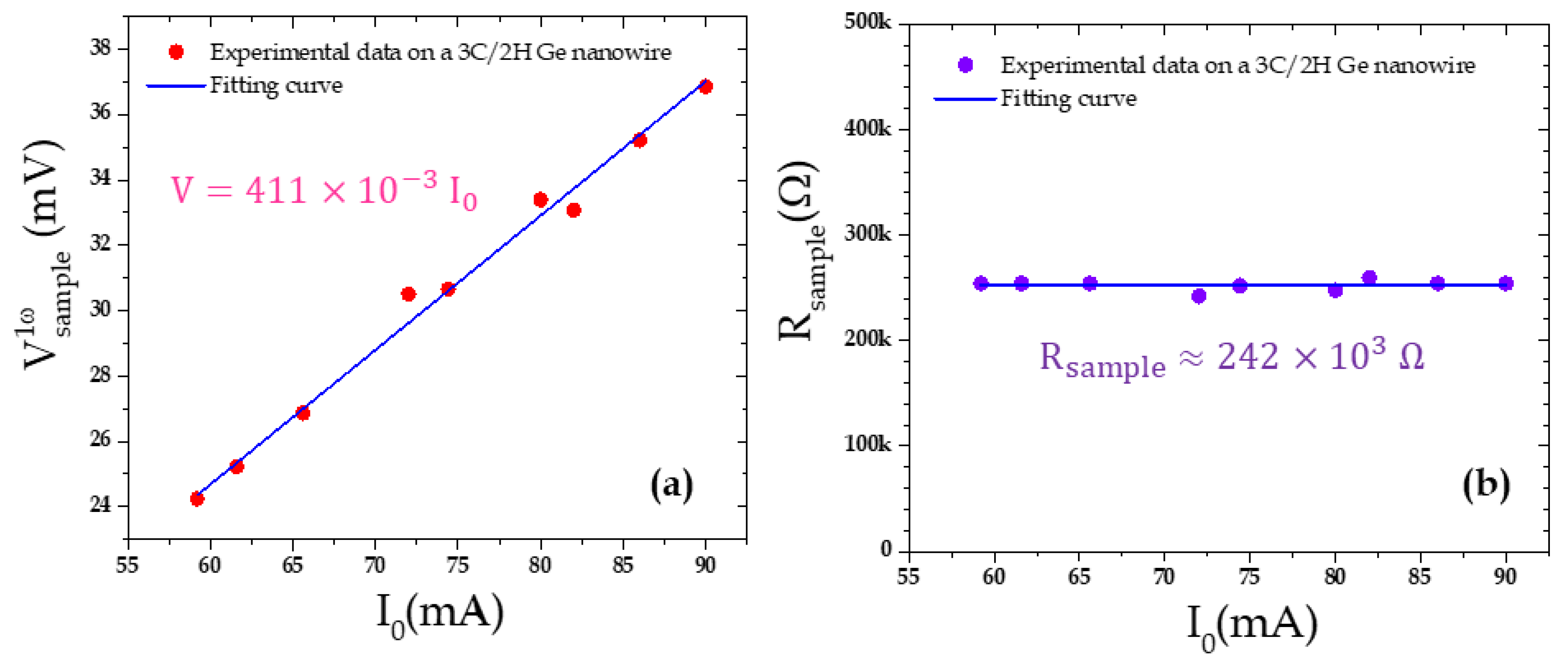
3.2. Electrical Measurements of Ge Nanowires
4. Conclusions
Supplementary Materials
Author Contributions
Funding
Institutional Review Board Statement
Informed Consent Statement
Data Availability Statement
Acknowledgments
Conflicts of Interest
References
- Goldberger, J.; Sirbuly, D.J.; Law, M.; Yang, P. ZnO nanowire transistors. J. Phys. Chem. B 2005, 109, 9–14. [Google Scholar] [CrossRef]
- Tomioka, K.; Yoshimura, M.; Fukui, T. A III–V nanowire channel on silicon for high-performance vertical transistors. Nature 2012, 488, 189–192. [Google Scholar] [CrossRef]
- Kouno, T.; Kishino, K.; Yamano, K.; Kikuchi, A. Two-dimensional light confinement in periodic InGaN/GaN nanocolumn arrays and optically pumped blue stimulated emission. Opt. Express 2009, 17, 20440–20447. [Google Scholar] [CrossRef]
- Waag, A.; Wang, X.; Fündling, S.; Ledig, J.; Erenburg, M.; Neumann, R.; Suleiman, M.A.; Merzsch, S.; Wei, J.; Li, S.; et al. The nanorod approach: GaN NanoLEDs for solid state lighting. Phys. Status Solidi C 2011, 8, 2296–2301. [Google Scholar] [CrossRef]
- Guler, U.; Shalaev, V.M.; Boltasseva, A. Nanoparticle plasmonics: Going practical with transition metal nitrides. Mater. Today 2015, 4, 227. [Google Scholar] [CrossRef]
- Peng, K.Q.; Lee, S.T. Silicon nanowires for photovoltaic solar energy conversion. Adv. Mater. 2011, 23, 198. [Google Scholar] [CrossRef]
- Holm, J.V.; Jørgensen, H.I.; Krogstrup, P.; Nygård, J.; Liu, H.; Aagesen, M. Surface-passivated GaAsP single-nanowire solar cells exceeding 10% efficiency grown on silicon. Nat. Commun. 2013, 4, 1498. [Google Scholar] [CrossRef]
- Calaza, C.; Salleras, M.; Davila, D.; Tarancon, A.; Morata, A.; Santos, J.D.; Gadea, G.; Fonseca, L. Bottom-up silicon nanowire arrays for thermoelectric harvesting. Mater. Today 2015, 2, 675. [Google Scholar] [CrossRef]
- Noyan, I.D.; Gadea, G.; Salleras, M.; Pacios, M.; Calaza, C.; Stranz, A.; Dolcet, M.; Morata, A.; Tarancon, A.; Fonseca, L. SiGe nanowire arrays based thermoelectric microgenerator. Nano Energy 2019, 57, 492. [Google Scholar] [CrossRef]
- Martin, P.N.; Aksamija, Z.; Pop, E.; Ravaiolo, U. Reduced thermal conductivity in nanoengineered rough Ge and GaAs nanowires. Nano Lett. 2010, 10, 1120–1124. [Google Scholar] [CrossRef] [PubMed]
- Wang, Z.; Mingo, N. Diameter dependence of SiGe nanowire thermal conductivity. Appl. Phys. Lett. 2010, 97, 101903. [Google Scholar] [CrossRef]
- Hochbaum, A.I.; Chan, R.; Delgado, R.D.; Liang, W.; Garnett, E.C.; Najarian, M.; Majumdar, A.; Yang, P. Enhanced thermoelectric performance of rough silicon nanowires. Nature 2008, 451, 163. [Google Scholar] [CrossRef]
- Whitesudes, G.M. Nanoscience, nanotechnology, and chemistry. Small 2015, 1, 172. [Google Scholar] [CrossRef]
- Heremans, J. Nanometer-scale thermoelectric materials. In Springer Handbook of Nanotechnology; Bhushan, B., Ed.; Springer: Berlin/Heidelberg, Germany, 2007; Volume 4–5, pp. 113–175. [Google Scholar]
- Lee, S.; Kim, L.; Kang, D.-H.; Meyyappan, M.; Baek, C.-K. Vertical silicon nanowire thermoelectric modules with enhanced thermoelectric properties. Nano Lett. 2019, 19, 747. [Google Scholar] [CrossRef]
- Dimmaggio, E.; Pennelli, G. Potentialities of silicon nanowire forests for thermoelectric generation. Nanotechnology 2018, 29, 135401. [Google Scholar] [CrossRef]
- Shi, L.; Li, D.; Yu, C.; Jang, W.; Kim, D.; Yao, Z.; Kim, P.; Majumdar, A. Measuring thermal and thermoelectric properties of one-dimensional nanostructures using a microfabricated device. J. Heat Trans. 2003, 125, 881. [Google Scholar] [CrossRef]
- Zhou, F.; Szczech, J.; Pettes, M.T.; Moore, A.L.; Jin, S.; Shi, L. Determination of transport properties in chromium disilicide nanowires via combined thermoelectric and structural characterizations. Nano Lett. 2007, 7, 1649. [Google Scholar] [CrossRef]
- Lee, P.-C.; Wei, P.-C.; Chen, Y.-Y. Thermoelectric characteristics of a single-crystalline topological insulator Bi2Se3 nanowire. Nanomaterials 2021, 11, 819. [Google Scholar]
- Moosavi, S.H.; Kojda, D.; Kockert, M.; Fischer, S.F.; Kroener, M.; Woias, P. The Effect of the MEMS measurement platform design on the seebeck coefficient measurement of a single nanowire. Nanomaterials 2018, 8, 219. [Google Scholar] [CrossRef] [PubMed]
- Vinaji, S.; Lochthofen, A.; Mertin, W.; Regolin, I.; Gutsche, C.; Prost, W.; Tegude, F.J.; Bacher, G. Material and doping transitions in single GaAs-based nanowires probed by Kelvin probe force microscopy. Nanotechnology 2009, 20, 385702. [Google Scholar] [CrossRef] [PubMed]
- Doerk, G.S.; Carraro, C.; Maboudian, R. Single nanowire thermal conductivity measurements by raman thermography. ACS Nano 2010, 4, 4908. [Google Scholar] [CrossRef]
- Ezzahri, Y.; Grauby, S.; Dilhaire, S.; Rampnoux, J.M.; Claeys, W. Cross-plan Si/SiGe superlattice acoustic and thermal properties measurement by picosecond ultrasonics. J. Appl. Phys. 2007, 101, 013705. [Google Scholar] [CrossRef]
- Rojo, M.M.; Calero, O.C.; Lopeandia, A.F.; Rodriguez-Viejo, J.; Martın-Gonzalez, M. Review on measurement techniques of transport properties of nanowires. Nanoscale 2013, 5, 11526. [Google Scholar] [CrossRef] [PubMed]
- Shi, L.; Zhou, J.; Kim, P.; Bachtold, A.; Majumdar, A.; McEuen, P.L. Thermal probing of energy dissipation in current-carrying carbon nanotubes. J. Appl. Phys. 2009, 105, 104306. [Google Scholar] [CrossRef]
- Hinz, M.; Marti, O.; Gotsmann, B.; Lantz, M.A.; Dürig, U. High resolution vacuum scanning thermal microscopy of HfO and SiO. Appl. Phys. Lett. 2008, 92, 043122. [Google Scholar] [CrossRef]
- Lefèvre, S.; Volz, S. 3ω-scanning thermal microscope. Rev. Sci. Instrum. 2005, 76, 033701. [Google Scholar] [CrossRef]
- Puyoo, E.; Grauby, S.; Rampnoux, J.-M.; Rouvière, E.; Dilhaire, S. Scanning thermal microscopy of individual silicon nanowires. J. Appl. Phys. 2011, 109, 024302. [Google Scholar] [CrossRef]
- Rojo, M.M.; Grauby, S.; Rampnoux, J.-M.; Caballero-Calero, O.; Martin-Gonzalez, M.; Dilhaire, S. Fabrication of Bi2Te3 nanowire arrays and thermal conductivity measurement by 3ω-scanning thermal microscopy. J. Appl. Phys. 2013, 113, 054308. [Google Scholar] [CrossRef]
- Rojo, M.M.; Martin, J.; Grauby, S.; Borca-Tasciuc, T.; Dilhaire, S.; Martin-Gonzalez, M. Decrease in thermal conductivity in polymeric P3HT nanowires by size-reduction induced by crystal orientation: New approaches towards thermal transport engineering of organic materials. Nanoscale 2014, 6, 7858. [Google Scholar] [CrossRef]
- Grauby, S.; Puyoo, E.; Rampnoux, J.-M.; Rouvière, E.; Dilhaire, S. Si and SiGe nanowires: Fabrication process and thermal conductivity measurement by 3ω-scanning thermal microscopy. J. Phys. Chem. C 2013, 117, 9025. [Google Scholar] [CrossRef]
- Amor, A.B.; Djomani, D.; Fakhfakh, M.; Dilhaire, S.; Vincent, L.; Grauby, S. Si and Ge allotrope heterostructured nanowires: Experimental evaluation of the thermal conductivity reduction. Nanotechnology 2019, 30, 375704. [Google Scholar] [CrossRef]
- Xu, K.Q.; Zeng, H.R.; Zhao, K.Y.; Li, G.R.; Shi, X.; Chen, L.D. Scanning near-field thermoelectric microscopy for subsurface nanoscale thermoelectric behavior. Appl. Phys. A 2016, 122, 521. [Google Scholar] [CrossRef]
- McGee, G.R.; Schankula, M.H.; Yovanovich, M.M. Thermal resistance of cylinder-flat contacts: Theoretical analysis and experimental verification of a line-contact model. Nucl. Eng. Des. 1985, 86, 369. [Google Scholar] [CrossRef]
- Kushvaha, S.S.; Hofbauer, W.; Loke, Y.C.; Singh, S.P.; O’Shea, S.J. Thermoelectric measurements using different tips in atomic force microscopy. J. Appl. Phys. 2011, 109, 084341. [Google Scholar] [CrossRef]
- Wilson, A.A.; Rojo, M.M.; Mayor, B.A.; Perez, J.A.; Maiz, J.; Schomacker, J.; Gonzalez, M.M.; Borca-Tasciuc, D.A.; Borca-Tasciuc, T. Thermal conductivity measurements of high and low thermal conductivity films using a scanning hot probe method in the 3ω mode and novel calibration strategies. Nanoscale 2015, 7, 154042. [Google Scholar] [CrossRef]
- Mason, S.J.; Hojem, A.; Wesenberg, D.J.; Avery, A.D.; Zink, B.L. Determining absolute Seebeck coefficients from relative thermopower measurements of thin films and nanostructures. J. Appl. Phys. 2020, 127, 085101. [Google Scholar] [CrossRef]
- Zhao, K.; Zeng, H.; Xu, K.; Yu, H.; Li, G.; Song, J.; Shi, X.; Chen, L. Scanning thermoelectric microscopy of local thermoelectric behaviors in (Bi,Sb)2Te3 films. Phys. B Condens. Matter 2015, 457, 156. [Google Scholar] [CrossRef]
- Zhang, Y.; Hapenciuc, C.; Castillo, E.; Tasciuc, T.B.; Mehta, R.; Karthik, C.; Ramanath, G. A microprobe technique for simultaneously measuring thermal conductivity and Seebeck coefficient of thin films. Appl. Phys. Lett. 2010, 96, 062107. [Google Scholar] [CrossRef]
- Ferrando-Villalba, P.; Pérez-Marín, A.P.; Abad, L.; Dalkiranis, G.G.; Lopeandia, A.F.; Garcia, G.; Rodriguez-Viejo, J. Measuring device and material ZT in a thin-film Si-based thermoelectric microgenerator. Nanomaterials 2019, 9, 653. [Google Scholar] [CrossRef] [PubMed]
- Puyoo, E.; Grauby, S.; Rampnoux, J.-M.; Rouvière, E.; Dilhaire, S. Thermal exchange radius measurement: Application to nanowire thermal imaging. Rev. Sci. Instrum. 2010, 81, 073701. [Google Scholar] [CrossRef] [PubMed]
- Gu, G.; Burghard, M.; Kim, G.T.; Dusberg, G.S.; Chiu, P.W.; Krstic, V.; Roth, S. Growth and electrical transport of germanium nanowires. J. Appl. Phys. 2001, 90, 5747. [Google Scholar] [CrossRef]
- Hanrath, T.; Korgel, B.A. Supercritical fluid–liquid–solid (SFLS) synthesis of Si and Ge nanowires seeded by colloidal metal nanocrystals. Adv. Mater. 2003, 15, 437–440. [Google Scholar] [CrossRef]
- Middleton, A.E.; Scanlon, W. Measurement of the thermoelectric power of germanium at temperatures above 78 °K. Phys. Rev. 1953, 92, 219. [Google Scholar] [CrossRef]
- Murphy-Armando, F. Enhancement of the electronic thermoelectric properties of bulk strained silicon-germanium alloys using the scattering relaxation times from first-principles calculations. J. Appl. Phys. 2019, 126, 215103. [Google Scholar] [CrossRef]
- Hui, W.L.C.; Corra, J.P. Seebeck coefficient of thin-film germanium. J. Appl. Phys. 1967, 38, 3477. [Google Scholar] [CrossRef]


Publisher’s Note: MDPI stays neutral with regard to jurisdictional claims in published maps and institutional affiliations. |
© 2021 by the authors. Licensee MDPI, Basel, Switzerland. This article is an open access article distributed under the terms and conditions of the Creative Commons Attribution (CC BY) license (https://creativecommons.org/licenses/by/4.0/).
Share and Cite
Grauby, S.; Ben Amor, A.; Hallais, G.; Vincent, L.; Dilhaire, S. Imaging Thermoelectric Properties at the Nanoscale. Nanomaterials 2021, 11, 1199. https://doi.org/10.3390/nano11051199
Grauby S, Ben Amor A, Hallais G, Vincent L, Dilhaire S. Imaging Thermoelectric Properties at the Nanoscale. Nanomaterials. 2021; 11(5):1199. https://doi.org/10.3390/nano11051199
Chicago/Turabian StyleGrauby, Stéphane, Aymen Ben Amor, Géraldine Hallais, Laetitia Vincent, and Stefan Dilhaire. 2021. "Imaging Thermoelectric Properties at the Nanoscale" Nanomaterials 11, no. 5: 1199. https://doi.org/10.3390/nano11051199
APA StyleGrauby, S., Ben Amor, A., Hallais, G., Vincent, L., & Dilhaire, S. (2021). Imaging Thermoelectric Properties at the Nanoscale. Nanomaterials, 11(5), 1199. https://doi.org/10.3390/nano11051199