Article

Atomic Defect Induced Saturable Absorption of Hexagonal Boron Nitride in Near Infrared Band for Ultrafast Lasing Applications

1
Shandong Provincial Key Laboratory of Optics and Photonic Devices, School of Physics and Electronics, Shandong Normal University, Jinan 250014, China
2
State Key Laboratory of Crystal Materials, School of Physics, Shandong University, Jinan 250100, China
3
Key Laboratory of Materials for High-Power Laser, Shanghai Institute of Optics and Fine Mechanics, Chinese Academy of Sciences, Shanghai 201800, China
*
Authors to whom correspondence should be addressed.
Nanomaterials 2021, 11(12), 3203; https://doi.org/10.3390/nano11123203
Submission received: 19 October 2021 / Revised: 13 November 2021 / Accepted: 24 November 2021 / Published: 26 November 2021
(This article belongs to the Special Issue Graphene and Related 2D Materials)

Abstract

:
Defect-induced phenomena in 2D materials has received increasing interest among researchers due to the novel properties correlated with precise modification of materials. We performed a study of the nonlinear saturable absorption of the boron-atom-vacancy defective hexagonal boron nitride (h-BN) thin film at a wavelength of ~1 μm and its applications in ultrafast laser generation. The h-BN is with wide band gap of ~6 eV. Our investigation shows that the defective h-BN has a wide absorption band from visible to near infrared regimes. First-principle calculations based on density functional theory (DFT) indicate that optical property changes may be attributed to the boron-vacancy-related defects. The photoluminescence spectrum shows a strong emission peak at ~1.79 eV. The ultrafast Z-scan measurement shows saturable absorbance response has been detected for the defective h-BN with saturation intensity of ~1.03 GW/cm2 and modulation depth of 1.1%. In addition, the defective h-BN has been applied as a new saturable absorber (SA) to generate laser pulses through the passively Q-switched mode-locking configuration. Based on a Nd:YAG waveguide platform, 8.7 GHz repetition rate and 55 ps pulse duration of the waveguide laser have been achieved. Our results suggest potential applications of defective h-BN for ultrafast lasing and integrated photonics.

1. Introduction

Artificial atomic defects in materials provide a powerful approach to establish physical systems for quantum technologies, including quantum communications, computing, information processing, etc. [1,2,3,4]. Up to now, they are widely applied in a few wide-bandgap (WBG) semiconductors such as diamond, ZnS, and silicon carbide [5,6,7,8,9,10]. With extended research of graphene, two-dimensional (2D) materials of single-atom-layer scale—such as transition metal dichalcogenides (TMDCs) or diselenides—have drawn great attention due to their layer-dependent properties for applications in various electronic and photonic devices [11,12]. Similarly to graphene, hexagonal boron nitride (h-BN) has a hexagonal honeycomb structure compound of boron and nitrogen atoms. Instead of the ultrahigh electrical conductivity of graphene, h-BN applies as an insulator with a wide bandgap of ~6 eV, which is of significant difference with the zero-direct-bandgap graphene [13,14,15,16,17,18,19,20,21]. The h-BN can be a complementary substrate to graphene and other 2D materials, which can effectively reduce the lattice mismatch and improve the uniformity of 2D materials such as graphene, and can also be used as an isolator at visible (VIS) and infrared (IR) wavelengths [16,17,22,23,24,25,26]. In addition, inducing defects in h-BN may overcome its shortcomings and enrich its applications in UV-VIS as well extend to longer-wavelength ranges [27,28,29,30]. Like other 2D materials, h-BN possesses fascinating photoluminescence (PL) and nonlinear optical (NLO) properties [14,31,32,33]. However, in defective h-BN, such properties correlated to the defects have not been fully explored yet. One of the most interesting NLO features of 2D atom-scale materials is the nonlinear saturable absorption, which is essential for the generation of ultrafast laser pulses through the passive Q-switching or mode-locking process [34,35,36]. The 2D-materials-based pulsed laser systems have been widely implemented in the laser platforms of bulks, fibers, and waveguides, in which a number of 2D materials—including graphene, TMDCs, topological insulators, black phosphorus, etc.—have been applied as efficient saturable absorbers (SA) [37,38,39,40,41,42,43]. As for h-BN, the wide bandgap of ~6 eV restricts its applications to a certain extent in long-wavelength regimes. Kumbhakar et al. reported UV-VIS NLO property of h-BN nanosheets and mentioned its possible saturable absorption in VIS band [27]. Kislyakov et al. reported two-photon absorption of h-BN in near infrared (NIR) [44]. Extension of applications to low-energy photon regimes can be realized by the introduction of defects in wide bandgap materials [29,45,46,47]. In fact, defect-engineered 2D layered materials have been applied in versatile areas with modified, or sometimes enhanced, properties in comparison to their perfect counterparts [48,49,50,51]. Cai et al. reported h-BN as SA material in a passively Q-switched erbium-doped fiber laser operating at 1.5 µm, in which they changed the ratio of boron atom and nitrogen atom [52]. In this work, we investigated the NLO properties of a defective h-BN in NIR wavelength band. The nonlinear saturable absorption of h-BN at near infrared wavelength (1 μm) has been observed, which is of potential applications for the NIR lasing. The mechanisms of such nonlinear saturable absorption in defective h-BN have been explored, which may be attributed to the boron-atom vacancy (Bv). We also further apply defective h-BN as a SA to generate ultrafast lasers at a 1 μm wavelength. The results herald that the applied range of Bv-defective h-BN can extend up to 2 μm; and Bv-defective h-BN may have a great potential to achieve on-chip integrated devices of ultrafast photonics

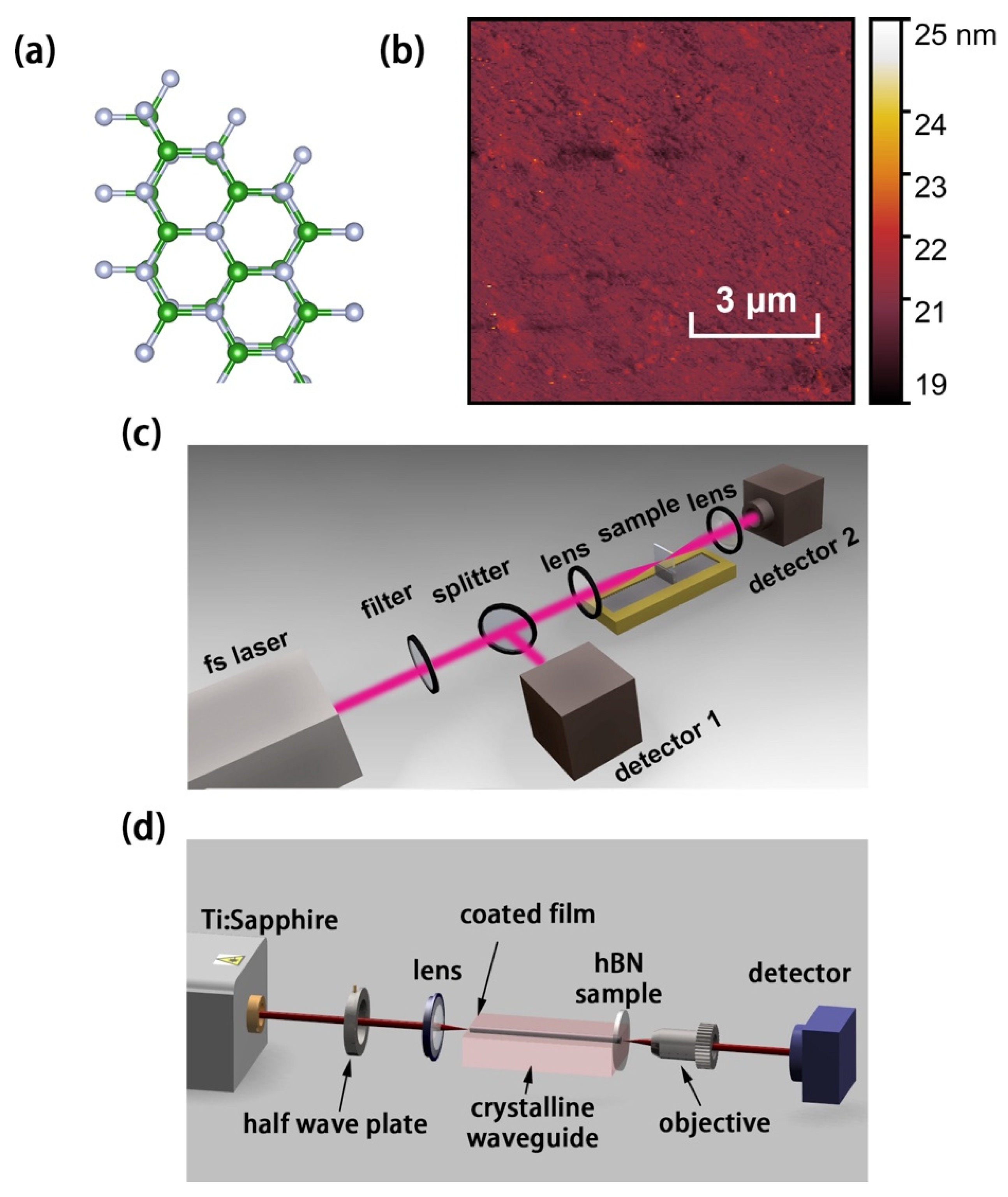
2. Materials and Methods

The defective h-BN thin film used in this work was customized from a chemical vendor (6Carbon Technology Co., Ltd., Shenzhen, China). It was made by chemical vapor deposition (CVD) technology, coated on a 10 × 10 mm2 surface of a sapphire wafer of which the faces were optically polished. The h-BN thin film was ensured to be consecutive and to cover all the face completely. Figure 1a shows a typical free-defect h-BN atomic structure that is very similar to hexagonal structure of graphene. An atomic force microscope (AFM) was utilized to characterize the defective h-BN thin film (shown in Figure 1b), by which it was observed that the thin film was with few wrinkles. Via AFM measurement, we obtained the height between the sapphire substrate and the sample surface, the value was approximately 13 nm. To investigate the crystalline structure, a home-made Raman spectral microscope was used to inspect the Raman scattering signal at 532 nm laser exciting. An optical microscope (Olympus BX43) connected with a fiber spectrometer (NOVA, Ideaoptics, Co., Ltd., Shanghai, China, 8 cm−1 resolution, 175 to 3100 cm−1) was employed to obtain the Raman spectrum of h-BN sample. A set of filters (cut-off at 186 cm−1, OD > 6 at 532 nm) was used to block the excitation light signal and to distinguish the scattered Raman signal. The detected region from 1000 cm−1 to 3000 cm−1 was set for measurement, including first- and second-order Raman-active spectra of the h-BN sample. As well as utilizing this microscope system, photoluminescence (PL) of the sample can be carried out via changing detective spectrometers (NOVA-EX, Ideaoptics, Co., Ltd., Shanghai, China, 1.98 μm resolution, 325 to 1100 nm) and filters. The 532-nm-wavelength laser was focused to be a spot with an approximate 1.5-μm diameter on the sample surface by an objective (100×, 0.8 N.A.). Additionally, this objective was used to collect Raman and PL signals into a 100-μm-diameter fiber. The h-BN sample was placed on a three-axis motorized stage (0.2-nm-resolution) of the microscope system.
For further investigation on the linear absorption, an absorption spectrum of the h-BN sample was measured by using a UV/VIS/NIR spectrophotometer (UV1800, Shimadzu, Kyoto, Japan) from 200 nm to 1100 nm, with a resolution of 1 nm. By this spectrophotometer, we performed measurement of not only the absorption, but also the transmittance and reflectance as functions of incidence wavelength.
For studying the nonlinear absorption of the h-BN sample, an open-aperture Z-scan system was used, that depicted in Figure 1c. In this system, the sample was mounted on a motorized translation stage to traverse the incident beam. The beam was focused by a 150 mm-focal-length lens. It was gradually moving, passing along the z-axis (laser propagation direction) for obtained the transmittance as a function of the incident laser intensity through the focus.
A waveguide laser platform was employed to study the saturable absorption of thin film as a SA in waveguide lasing, shown in Figure 1d. The platform is built by a Nd:YAG crystalline waveguide (doped by 1 at % Nd3+ ions), fabricated by the femtosecond laser writing and coated optical film [39,53]. A 30 mm-focal-length lens was used to launch the pump beam. Additionally, a 20× and 0.4-N.A. microscope objective was used to collect the output lasers. A tunable CW Ti:Sapphire laser (Coherent MBR PE) generates optical pump beam with a linearly polarized light beam at 810 nm wavelength. The h-BN sample is covered on an output coupler mirror. The mirror and h-BN sample were pressed close to the end-face of the waveguide. The detective devices were located after the objective lens at the end of the waveguide lasing system, including a fast photodiode, a power meter, a spectrometer, etc.

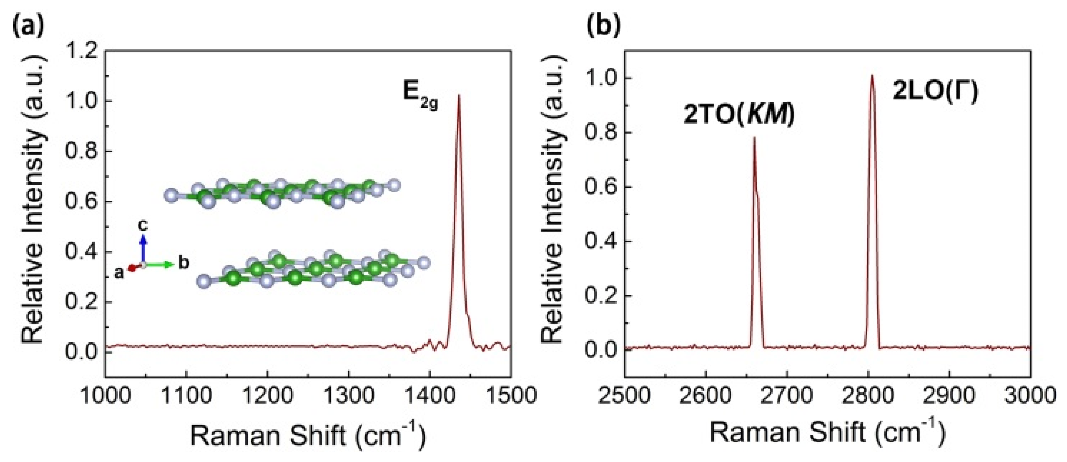
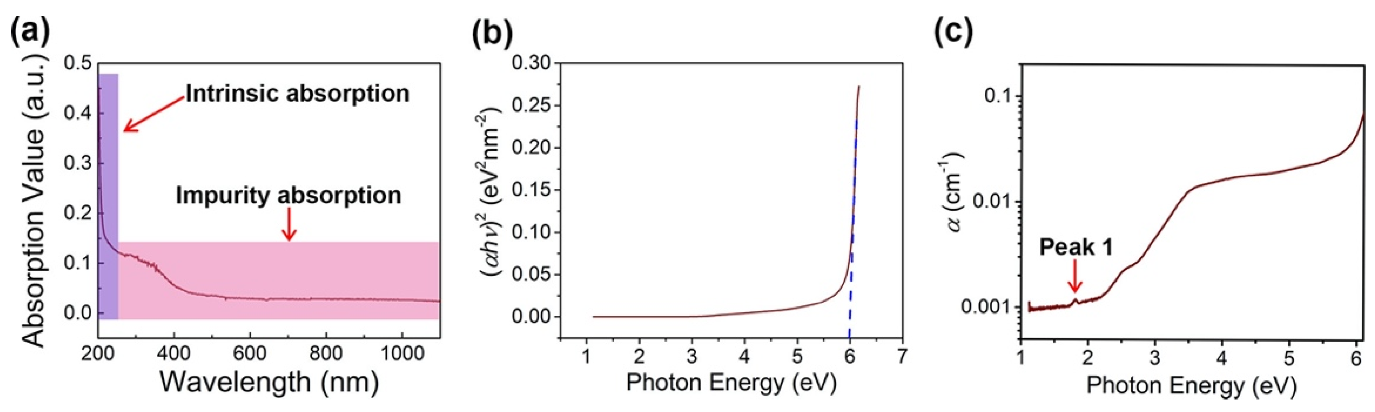
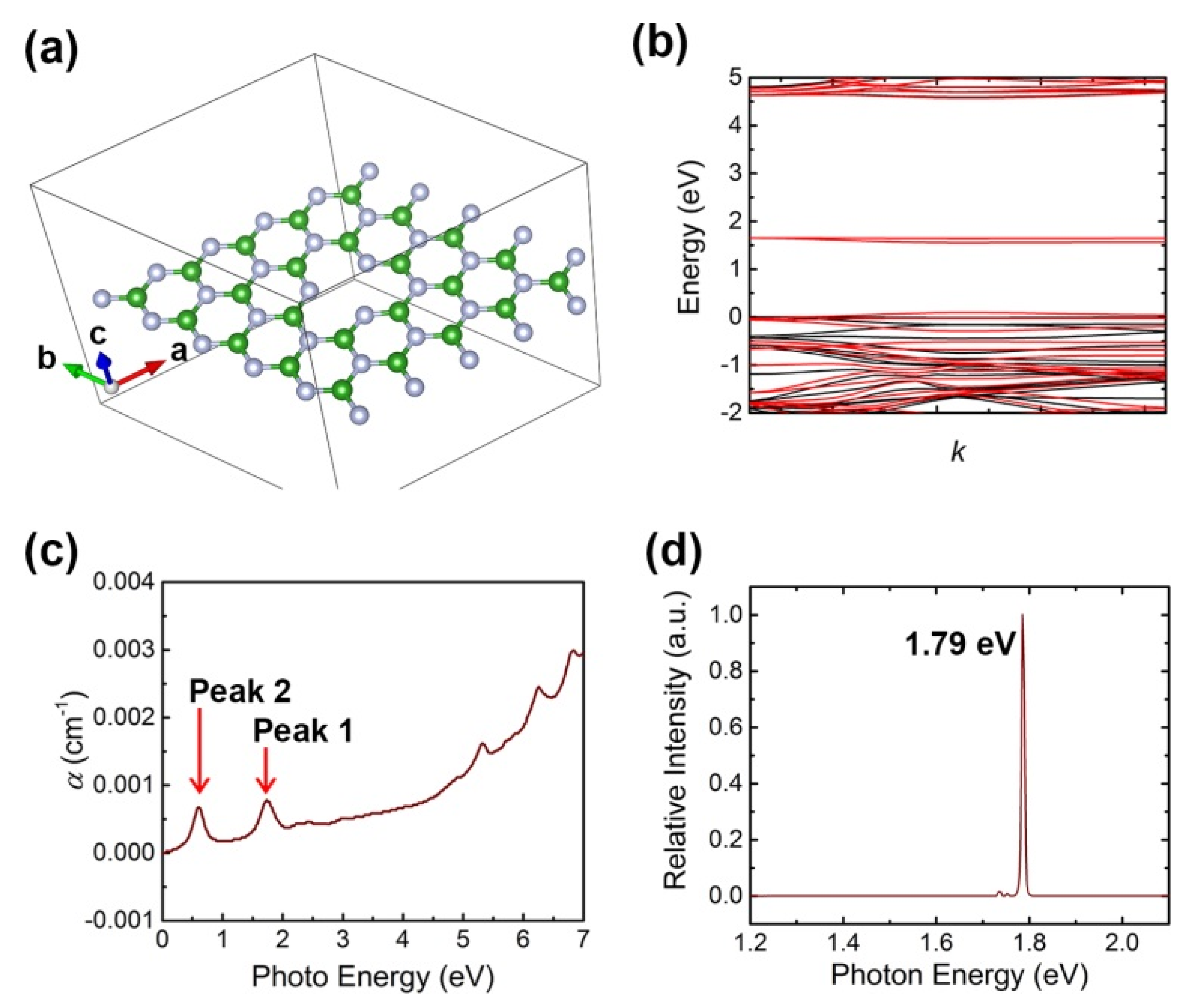
3. Results and Discussion

Figure 2a shows the first-order Raman spectrum of h-BN sample excited with 532 nm. The inset displays the crystalline structure of bi-layer h-BN prototype. The atomic displacements of boron and the nitrogen atoms in each plane move in opposite directions symmetrically that give to a Raman-active peak, as well without LO-TO splitting since the contributions from the two planes cancel each other [54,55]. Accordingly, this typical h-BN high-energy peak appeared at 1435.4 cm−1. This peak demonstrated an in-plane optical mode with the E2g or Г symmetry, which differed from two peaks of c-BN. The second-order Raman spectrum has been shown in Figure 2b, in the range from 2500 cm−1 to 3000 cm−1. Two peaks have appeared at 2661 cm−1 and 2805.1 cm−1, which corresponded to 2TO mode and were twice the frequency of the Raman-active Г point mode. These three peaks are consistent with the previous report and characterized a typical h-BN sample [54,56].
A linear absorbed spectrum with the wavelength from 200 nm to 1100 nm is shown in Figure 3a. In this spectrum, it can obviously find that the intense impurity absorption appeared from the VIS band to NIR band. Figure 3b shows the (αhν)2- spectrum of the h-BN sample based on Tauc’s plot [57]. By drawing a tangent line in the linear region of the spectrum, the line is extrapolated to -axis. The intercept of ~6 eV was obtained for this sample, that the value would be the direct band-gap of the h-BN sample. The result is in agreement with the previous works [58]. The linear absorbed coefficient α has a relationship with the transmittance T and thickness d of the sample, which can be expressed as
α = ln ( 1 / T ) / d
The calculated linear absorbed coefficient α is a function of photon energy, which has been shown in Figure 3c. In this spectrum, there are a few absorbed impurity energy levels appearing at from VIS to NIR regions, in which a peak is marked in the figure as Peak 1 at 1.8 eV.
To reveal the origin of impurity absorption, we use first-principle calculations based on density function theory (DFT) to investigate the defects using the Vienna ab initio simulation package (VASP) with the Perdew–Burke–Ernzerhof (PBE) exchange-correlation functional. The plane wave was set to the cut-off energy of 500 eV. All atoms were allowed to relax until the Hellmann–Feynman forces reached the convergence criterion of less than 0.01 eV/Å. The convergence threshold of energy was set at 10−5 eV. The Monkhorst-Pack scheme was used to sample k-points in the Brillouin zone. After a few calculations of possible defective structures, a Bv defect was considered in the h-BN sample, which played a main part in the impurity absorption. Figure 4a shows the Bv-defective h-BN structure of a unit cell and the detailed defective structures are shown in Figure S1 and Figure S2 (Supplementary Materials). The spin-polarized band structures of BN with single B-vacancy are shown in Figure 4b, in which the Fermi level has been set to zero. Spin-up and spin-down structures are represented by red and black lines. According to projector-augmented wave (PAW) method that the light is vertical respect to the plane of BN, and then the imaginary part ε2 of dielectric is determined by summation of all possible hopping processes [59]
ε 2 = 4 π 2 e 2 S c , v , k 2 ω δ ( ( ϵ c k ϵ v k ) ω ) u c k | u v k u v k | u c k
and the real part ε1 can be deduced by usual Kramers–Kronig transformation
ε 1 = 1 + 2 π P 0 ε 2 ( ω ) ω d ω ω 2 ω 2 + i η
with these two, the absorption coefficients are given by
I = 2 ω ε 1 2 + ε 2 2 ε 1
Finally, we obtain a calculated spectrum of a function between photo energy and linear absorption coefficient α, which was shown in Figure 4c, the absorptions of other defective structures are shown in Figure S3 (Supplementary Materials). In this spectrum, two absorption peaks at ~1.8 eV and ~0.6 eV were labeled. Figure 4d shows PL spectrum excited with 532 nm. In this condition, a bright emission peak is detected at 1.79 eV (624 nm).
In nonlinear absorption regions, conspicuous saturable absorption can be detected under incident 30–150 nJ femtosecond laser pulse in the Z-scan system. The original Z-scan data are shown in the Figure S4 (Supplementary Materials). The results were recalculated to be a function between incident fluence and transmission and are demonstrated in Figure 5a–d. The maximum incident energy was set to be 150 nJ, which was corresponding up to 160.3 GW/cm2 (z = 0). Despite being under such higher incident fluence, the defective h-BN exhibits a stable nonlinear performance, even though we repeated the Z-scan experiment continuously more than 10 times.
Based on the propagation theory, a differential equation in the thin film can be written as [34]
d I d z = α ( I ) I
where z′ is the propagation distance in the samples, I is the input intensity.
For nonlinear saturable absorption response, we can also describe the total absorption coefficient α(I) in Equation (1), the saturable absorption model, with the form of [60]
α ( I ) = α 0 1 + I / I S
where α0 is linear absorption coefficient, and Is is the saturable intensity. Normally, the normalized transmittance in the Z-scan measurement is
T = ( 1 α 0 1 + I / I S ) / ( 1 α 0 d )
From the fitting curves based on Equation (7), a perfect saturable absorption data fitting can be found; the saturable intensity and modulation depth (α0d) are about 1.03 ± 0.01 GW/cm2 and 1.10% at 1030 nm.
Using the waveguide lasing platform, a Q-switched pulsed laser was achieved under optical pump, with an SA of Bv-defective h-BN thin film. The working wavelength of waveguide lasing is 1064 nm (1.16 eV) for both TE- and TM-polarization. Figure 6a shows the repetition rates and pulse durations as a function of launched power at two orthogonal TE and TM polarizations. The maximum repetition rate values were 2.421 MHz and 2.481 MHz at TE- and TM-polarization, respectively. The minimum pulse duration values were as fast as 133 ns (158 ns) pumping at TE- (TM-) polarized laser. The pulse energy and peak power, as shown in Figure 6b, increased significantly as the incident pump power increased, from 0.5 nJ to 32.4 nJ (from 7.6 nJ to 35.0 nJ), in TE (TM) polarized light pumping, respectively. Figure 6b shows that the laser performance is unstable in areas where the pump power is higher than 0.85 W. High-power pump lasers may cause strong thermal effects, which may change the nonlinear performance of defective h-BN. The two-dimensional material SAs controlled by the defect state may have a broader application in integrated waveguide lasers and fiber lasers driven by lower optical power.
By further adjusting the resonant cavity of the waveguide lasing platform, a Q-switched mode-locked (QML) pulsed laser was obtained on the basis of the original Q-switched pulsed laser. The fast photodetector connected to the oscilloscope acquires the pulse signal of the mode-locked pulsed laser, as shown in Figure 6c,d. In Figure 6d, the mode-locked pulse has a repetition rate of 8.7 GHz and a pulse width of 55 ps. According to the selected linear Fabry–Pérot waveguide laser resonator, the repetition frequency of the laser oscillation in the cavity can be expressed as: f = c·2nl, where c (m·s−1) is the speed of light, n is the refractive index of the waveguide material, and l is the length of the cavity. The theoretical calculation repetition frequency f is ~8.7 GHz, which is consistent with the experimental results. Compared with graphene and other 2D materials SAs, the Bv-defective h-BN performs a fairly level lasing field. One percent modulation depth of Bv-detective h-BN is very similar to numerical values of most 2D materials, for example 1.1%- 1.8%-, and 0.8%-modulation-depth of graphene, WS2, and black phosphorous, respectively [61,62]. With pulse durations in picoseconds—for example 52 ps, 43 ps, 26 ps—CVD graphene, MoS2, and BiSe2, were obtained in QML regime [63]. In the results of DFT calculations, it can be speculated that the Bv-defective h-BN has a great potential in near 2 μm applications, which can be a complementary SA candidate of graphene SA [64].
Given the above results, it can be inferred that a series of Bv-detective energy levels are near the Fermi level of the h-BN sample, shown in Figure 7a. In this figure, four processes were labeled, which were E1 → E2, E0 → E2, E2 → E0, E0 → E1, respectively. According to the impurity absorption spectrum, E2 energy level is in the position of the impurity energy band. Process II and III have been described the impurity absorption process, which is corresponding to the cause of inducing Peak 1 in Figure 3c. The PL emission peak of 1.79 eV also can verify the existence of E2 energy level. The process III has been proved by calculation of Kramers–Kronig transformation, which also implied Bv-defective h-BN have applied potential in the NIR band of 2 μm. Based on the above processes, it may be inferred that a two-level system can be used to explain the saturable absorbed responses of defective h-BN, as shown in Figure 7b. In the figure, we labeled the process of absorption at working wavelength (1064 nm) in orange. In this system, when the h-BN sample was illuminated by the working laser, process IV occurred. When the intensity increased to the threshold of saturable absorption, excited state absorption would occur and induce the transition of E1 → E2 by a rapid depletion of the ground valence states. Accordingly, the number of electrons, which were in the ground state, approached zero. Then the h-BN sample no longer absorbed the working laser, so that it reached saturation and became transparent at the working wavelength.

4. Conclusions

To summarize, we have unveiled nonlinear saturable absorption from single-atomic defect of boron vacancy in two-dimensional h-BN. The single-atomic defect has caused a series of impurity absorption from VIS to NIR bands, as well induced a bright PL peak at 1.79 eV at room temperature. We used Z-scan technology to demonstrate the nonlinear saturable absorption of the defective h-BN at ~1 μm. Defective h-BN has a saturable intensity of 1.03 ± 0.01 GW/cm2 and a modulation depth of 1.10% at 1030 nm. Based on a Nd:YAG crystalline waveguide platform, the Q-switched mode-locking laser has been achieved with a 8.7 GHz repetition rate and 55 ps pulse duration. Our results improve the scientific and technological importance of artificial atom-defect in 2D materials, in particular h-BN. These will be a solid foundation for new ultrafast applications in photonic technologies and optoelectronics based on 2D materials, highlighting the great potential of h-BN devices.

Supplementary Materials

The following are available online at https://www.mdpi.com/article/10.3390/nano11123203/s1, Figure S1: Chemical bond lengths (in Angstroms) in the Bv-defective hBN. The boron and nitrogen atoms are represented by green and grey balls respectively; Figure S2: The geometry structure of BN with (a) one N-atom vacancy, (b) B-atom vacancy and BN substitution, (c) N-atom vacancy and NB substitution. Red arrows mark the substitution sites; Figure S3: The calculated absorption coefficients of (a) Nv-defective, (b) NvBN-defective, and (c) BvNB-defective h-BN; Figure S4: Non-linear absorption responses detected by Z-scan system with (a) 50 μJ, (b) 80 μJ, (c) 100 μJ, and (d) 150 μJ incident intensities.

Author Contributions

Conceptualization and methodology, C.C. and R.L.; Z-scan test, Z.L. and N.D.; Writing—original draft preparation, C.C.; Writing—review and editing, F.C.; Supervision and project administration, J.W. and F.C. All authors have read and agreed to the published version of the manuscript.

Funding

National Natural Science Foundation of China (11904212, 11535008, 61522510); China Postdoctoral Science Foundation (2019M662455).

Institutional Review Board Statement

Not applicable.

Data Availability Statement

Data underlying the results presented in this paper are not publicly available at this time but may be obtained from the authors upon reasonable request.

Conflicts of Interest

The authors declare no conflict of interest.

References

  1. O’brien, J.L.; Furusawa, A.; Vučković, J. Photonic quantum technologies. Nat. Photonics 2009, 3, 687–695. [Google Scholar] [CrossRef] [Green Version]
  2. Awschalom, D.D.; Bassett, L.C.; Dzurak, A.S.; Hu, E.L.; Petta, J.R. Quantum spintronics: Engineering and manipulating atom-like spins in semiconductors. Science 2013, 339, 1174–1179. [Google Scholar] [CrossRef] [Green Version]
  3. Wrachtrup, J.; Jelezko, F. Processing quantum information in diamond. J. Phys. Condens. Matter 2006, 18, S807. [Google Scholar] [CrossRef]
  4. Maurer, P.C.; Kucsko, G.; Latta, C.; Jiang, L.; Yao, N.Y.; Bennett, S.D.; Pastawski, F.; Hunger, D.; Chisholm, N.; Markham, M.; et al. Room-temperature quantum bit memory exceeding one second. Science 2012, 336, 1283–1286. [Google Scholar] [CrossRef] [PubMed] [Green Version]
  5. Hao, X.; Wang, Y.; Zhou, J.; Cui, Z.; Wang, Y.; Zou, Z. Zinc vacancy-promoted photocatalytic activity and photostability of ZnS for efficient visible-light-driven hydrogen evolution. Appl. Catal. B Environ. 2018, 221, 302–311. [Google Scholar] [CrossRef]
  6. Batalov, A.; Jacques, V.; Kaiser, F.; Siyushev, P.; Neumann, P.; Rogers, L.J.; McMurtrie, R.L.; Manson, N.B.; Jelezko, F.; Wrachtrup, J. Low temperature studies of the excited-state structure of negatively charged nitrogen-vacancy color centers in diamond. Phys. Rev. Lett. 2009, 102, 195506. [Google Scholar] [CrossRef] [PubMed] [Green Version]
  7. Falk, A.L.; Klimov, P.V.; Buckley, B.B.; Ivády, V.; Abrikosov, I.A.; Calusine, G.; Koehl, W.F.; Gali, Á.; Awschalom, D.D. Electrically and mechanically tunable electron spins in silicon carbide color centers. Phys. Rev. Lett. 2014, 112, 187601. [Google Scholar] [CrossRef] [PubMed] [Green Version]
  8. Widmann, M.; Lee, S.Y.; Rendler, T.; Son, N.T.; Fedder, H.; Paik, S.; Yang, L.-P.; Zhao, N.; Yang, S.; Booker, I. Coherent control of single spins in silicon carbide at room temperature. Nat. Mater. 2015, 14, 164–168. [Google Scholar] [CrossRef] [Green Version]
  9. Klimov, P.V.; Falk, A.L.; Buckley, B.B.; Awschalom, D.D. Electrically driven spin resonance in silicon carbide color centers. Phys. Rev. Lett. 2014, 112, 087601. [Google Scholar] [CrossRef] [Green Version]
  10. Simin, D.; Fuchs, F.; Kraus, H.; Sperlich, A.; Baranov, P.G.; Astakhov, G.V.; Dyakonov, V. High-precision angle-resolved magnetometry with uniaxial quantum centers in silicon carbide. Phys. Rev. Appl. 2015, 4, 014009. [Google Scholar] [CrossRef] [Green Version]
  11. Sun, Z.; Martinez, A.; Wang, F. Optical modulators with 2D layered materials. Nat. Photonics 2016, 10, 227–238. [Google Scholar] [CrossRef] [Green Version]
  12. Li, X.; Zhu, M.; Du, M.; Lv, Z.; Zhang, L.; Li, Y.; Yang, Y.; Yang, T.; Li, X.; Wang, K.; et al. High detectivity graphene-silicon heterojunction photodetector. Small 2016, 12, 595–601. [Google Scholar] [CrossRef]
  13. Song, L.; Ci, L.; Lu, H.; Sorokin, P.B.; Jin, C.; Ni, J.; Kvashnin, A.G.; Kvashnin, D.G.; Lou, J.; Yakobson, B.I.; et al. Large scale growth and characterization of atomic hexagonal boron nitride layers. Nano Lett. 2010, 10, 3209–3215. [Google Scholar] [CrossRef]
  14. Watanabe, K.; Taniguchi, T.; Kanda, H. Direct-bandgap properties and evidence for ultraviolet lasing of hexagonal boron nitride single crystal. Nat. Mater. 2004, 3, 404–409. [Google Scholar] [CrossRef] [PubMed]
  15. Kubota, Y.; Watanabe, K.; Tsuda, O.; Taniguchi, T. Deep ultraviolet light-emitting hexagonal boron nitride synthesized at atmospheric pressure. Science 2007, 317, 932–934. [Google Scholar] [CrossRef] [PubMed] [Green Version]
  16. Li, L.J.; O’Farrell, E.C.T.; Loh, K.P.; Eda, G.; Ozyilmaz, B.; Neto, A.H.C. Controlling many-body states by the electric-field effect in a two-dimensional material. Nature 2016, 529, 185–189. [Google Scholar] [CrossRef] [PubMed] [Green Version]
  17. Cadiz, F.; Courtade, E.; Robert, C.; Wang, G.; Shen, Y.; Cai, H.; Taniguchi, T.; Watanabe, K.; Carrere, H.; Lagarde, D.; et al. Excitonic linewidth approaching the homogeneous limit in MoS2-based van der Waals heterostructures. Phys. Rev. X 2017, 7, 021026. [Google Scholar] [CrossRef] [Green Version]
  18. Muñoz, A.D.O.; Escobedo-Morales, A.; Skakerzadeh, E.; Chigo Anota, E. Effect of homonuclear boron bonds in the adsorption of DNA nucleobases on boron nitride nanosheets. J. Mol. Liq. 2021, 322, 114951. [Google Scholar] [CrossRef]
  19. Chigo Anota, E.; Escobedo-Morales, A.; Salazar Villanueva, M.; Vázquez-Cuchillo, O.; Rosas, E.R. On the influence of point defects on the structural and electronic properties of graphene-like sheets: A molecular simulation study. J. Mol. Model. 2013, 19, 839–846. [Google Scholar] [CrossRef]
  20. Jha, P.K.; Soni, H.R. Strain induced modification in phonon dispersion curves of monolayer boron pnictides. J. Appl. Phys. 2014, 115, 023509. [Google Scholar] [CrossRef]
  21. Sharma, V.; Kagdada, H.L.; Jha, P.K.; Śpiewak, P.; Kurzydłowski, K.J. Thermal transport properties of boron nitride based materials: A review. Renew. Sustain. Energy Rev. 2020, 120, 109622. [Google Scholar] [CrossRef]
  22. Cassabois, G.; Valvin, P.; Gil, B. Hexagonal boron nitride is an indirect bandgap semiconductor. Nat. Photonics 2016, 10, 262–266. [Google Scholar] [CrossRef] [Green Version]
  23. Lee, G.H.; Yu, Y.J.; Cui, X.; Petrone, N.; Lee, C.-H.; Choi, M.S.; Lee, D.-Y.; Lee, C.; Yoo, W.J.; Watanabe, K. Flexible and transparent MoS2 field-effect transistors on hexagonal boron nitride-graphene heterostructures. ACS Nano 2013, 7, 7931–7936. [Google Scholar] [CrossRef]
  24. Xue, J.; Sanchez-Yamagishi, J.; Bulmash, D.; Jacquod, P.; Deshpande, A.; Watanabe, K.; Taniguchi, T.; Jarillo-Herrero, P.; LeRoy, B.J. Scanning tunnelling microscopy and spectroscopy of ultra-flat graphene on hexagonal boron nitride. Nat. Mater. 2011, 10, 282–285. [Google Scholar] [CrossRef] [PubMed] [Green Version]
  25. Yankowitz, M.; Xue, J.; LeRoy, B.J. Graphene on hexagonal boron nitride. J. Phys. Condens. Matter 2014, 26, 303201. [Google Scholar] [CrossRef] [PubMed] [Green Version]
  26. Yankowitz, M.; Xue, J.; Cormode, D.; Sanchez-Yamagishi, J.D.; Watanabe, K.; Taniguchi, T.; Jarillo-Herrero, P.; Jacquod, P.; LeRoy, B.J. Emergence of superlattice Dirac points in graphene on hexagonal boron nitride. Nat. Phys. 2012, 8, 382–386. [Google Scholar] [CrossRef] [Green Version]
  27. Kumbhakar, P.; Kole, A.K.; Tiwary, C.S.; Biswas, S.; Vinod, S.; Taha-Tijerina, J.; Chatterjee, U.; Ajayan, P.M. Nonlinear optical properties and temperature-dependent UV–vis absorption and photoluminescence emission in 2D hexagonal boron nitride nanosheets. Adv. Opt. Mater. 2015, 3, 828–835. [Google Scholar] [CrossRef]
  28. Tran, T.T.; Elbadawi, C.; Totonjian, D.; Lobo, C.J.; Grosso, G.; Moon, H.; Englund, D.R.; Ford, M.J.; Aharonovich, I.; Toth, M. Robust multicolor single photon emission from point defects in hexagonal boron nitride. ACS Nano 2016, 10, 7331–7338. [Google Scholar] [CrossRef]
  29. Tran, T.T.; Bray, K.; Ford, M.J.; Toth, M.; Aharonovich, I. Quantum emission from hexagonal boron nitride monolayers. Nat. Nanotechnol. 2016, 11, 37–41. [Google Scholar] [CrossRef]
  30. Bourrellier, R.; Meuret, S.; Tararan, A.; Stéphan, O.; Kociak, M.; Tizei, L.H.G.; Zobelli, A. Bright UV single photon emission at point defects in h-BN. Nano Lett. 2016, 16, 4317–4321. [Google Scholar] [CrossRef]
  31. Watanabe, K.; Taniguchi, T.; Niiyama, T.; Miya, K.; Taniguchi, M. Far-ultraviolet plane-emission handheld device based on hexagonal boron nitride. Nat. Photonics 2009, 3, 591–594. [Google Scholar] [CrossRef]
  32. Silly, M.G.; Jaffrennou, P.; Barjon, J.; Lauret, J.-S.; Ducastelle, F.; Loiseau, A.; Obraztsova, E.; Attal-Tretout, B.; Rosencher, E. Luminescence properties of hexagonal boron nitride: Cathodoluminescence and photoluminescence spectroscopy measurements. Phys. Rev. B 2007, 75, 085205. [Google Scholar] [CrossRef]
  33. Museur, L.; Anglos, D.; Petitet, J.P.; Michel, J.P.; Kanaev, A.V. Photoluminescence of hexagonal boron nitride: Effect of surface oxidation under UV-laser irradiation. J. Lumin. 2007, 127, 595–600. [Google Scholar] [CrossRef] [Green Version]
  34. Wang, K.; Wang, J.; Fan, J.; Lotya, M.; O’Neill, A.; Fox, D.; Feng, Y.; Zhang, X.; Jiang, B.; Zhao, Q.; et al. Ultrafast saturable absorption of two-dimensional MoS2 nanosheets. ACS Nano 2013, 7, 9260–9267. [Google Scholar] [CrossRef]
  35. Zheng, Z.; Zhao, C.; Lu, S.; Chen, Y.; Li, Y.; Zhang, H.; Wen, S. Microwave and optical saturable absorption in graphene. Opt. Express 2012, 20, 23201–23214. [Google Scholar] [CrossRef] [PubMed]
  36. Zhao, X.; Liu, Z.B.; Yan, W.B.; Wu, Y.; Zhang, X.L.; Chen, Y.; Tian, J.G. Ultrafast carrier dynamics and saturable absorption of solution-processable few-layered graphene oxide. Appl. Phys. Lett. 2011, 98, 121905. [Google Scholar] [CrossRef]
  37. Zhang, S.; Li, Y.; Zhang, X.; Dong, N.; Wang, K.; Hanlon, D.; Coleman, J.N.; Zhang, L.; Wang, J. Slow and fast absorption saturation of black phosphorus: Experiment and modelling. Nanoscale 2016, 8, 17374–17382. [Google Scholar] [CrossRef] [PubMed]
  38. Bao, Q.; Zhang, H.; Wang, Y.; Ni, Z.; Yan, Y.; Shen, Z.X.; Loh, K.P.; Tang, D.Y. Atomic-layer graphene as a saturable absorber for ultrafast pulsed lasers. Adv. Funct. Mater. 2009, 19, 3077–3083. [Google Scholar] [CrossRef]
  39. Cheng, C.; Li, Z.; Dong, N.; Wang, J.; Chen, F. Tin diselenide as a new saturable absorber for generation of laser pulses at 1 μm. Opt. Express 2017, 25, 6132–6140. [Google Scholar] [CrossRef]
  40. Li, R.; Dong, N.; Cheng, C.; Ren, F.; Huebner, R.; Wang, J.; Zhou, S.; Chen, F. Giant enhancement of nonlinear optical response in Nd: YAG single crystals by embedded silver nanoparticles. ACS Omega 2017, 2, 1279–1286. [Google Scholar] [CrossRef] [PubMed]
  41. Luo, Z.; Huang, Y.; Weng, J.; Cheng, H.; Lin, Z.; Xu, B.; Cai, Z.; Xu, H. 1.06 μm Q-switched ytterbium-doped fiber laser using few-layer topological insulator Bi2Se3 as a saturable absorber. Opt. Express 2013, 21, 29516–29522. [Google Scholar] [CrossRef] [PubMed]
  42. Chen, Y.; Jiang, G.; Chen, S.; Guo, Z.; Yu, X.; Zhao, C.; Zhang, H.; Bao, Q.; Wen, S.; Tang, D.; et al. Mechanically exfoliated black phosphorus as a new saturable absorber for both Q-switching and mode-locking laser operation. Opt. Express 2015, 23, 12823–12833. [Google Scholar] [CrossRef] [Green Version]
  43. Xian, Y.; Cai, Y.; Sun, X.; Liu, X.; Guo, Q.; Zhang, Z.; Tong, L.; Qiu, J. Refractory Plasmonic Metal Nitride Nanoparticles for Broadband Near-Infrared Optical Switches. Laser Photonics Rev. 2019, 13, 1900029. [Google Scholar] [CrossRef]
  44. Kislyakov, I.M.; Nunzi, J.M.; Zhang, X.; Xie, Y.; Bocharov, V.N.; Wang, J. Competition between stimulated Brillouin scattering and two-photon absorption in dispersed boron nitride. Opt. Express 2019, 27, 11029–11036. [Google Scholar] [CrossRef]
  45. Van De Walle, C.G. (Ed.) Wide-Band-Gap Semiconductors; North-Holland: Amsterdam, The Netherlands, 1993. [Google Scholar]
  46. Yu, X.; Yu, P.; Wu, D.; Singh, B.; Zeng, Q.; Lin, H.; Zhou, W.; Lin, J.; Suenaga, K.; Liu, Z.; et al. Atomically thin noble metal dichalcogenide: A broadband mid-infrared semiconductor. Nat. Commun. 2018, 9, 1545. [Google Scholar] [CrossRef] [PubMed]
  47. Liu, Y.; Wang, G.; Wang, S.; Yang, J.; Chen, L.; Qin, X.; Song, B.; Wang, B.; Chen, X. Defect-induced magnetism in neutron irradiated 6H-SiC single crystals. Phys. Rev. Lett. 2011, 106, 087205. [Google Scholar] [CrossRef] [Green Version]
  48. Jiménez, I.; Jankowski, A.F.; Terminello, L.J.; Sutherland, D.G.J.; Carlisle, J.A.; Doll, G.L.; Tong, W.M.; Shuh, D.K.; Himpsel, F.J. Core-level photoabsorption study of defects and metastable bonding configurations in boron nitride. Phys. Rev. B 1997, 55, 12025. [Google Scholar] [CrossRef] [Green Version]
  49. Wang, V.; Ma, N.; Mizuseki, H.; Kawazoe, Y. First-principles study of intrinsic defect properties in hexagonal BN bilayer and monolayer. Solid State Commun. 2012, 152, 816–820. [Google Scholar] [CrossRef]
  50. Tan, Y.; Guo, Z.; Shang, Z.; Liu, F.; Böttger, R.; Zhou, S.; Shao, J.; Yu, X.; Zhang, H.; Chen, F. Tailoring nonlinear optical properties of Bi2Se3 through ion irradiation. Sci. Rep. 2016, 6, 21799. [Google Scholar] [CrossRef] [PubMed] [Green Version]
  51. Li, Z.; Chen, F. Ion beam modification of two-dimensional materials: Characterization, properties, and applications. Appl. Phys. Rev. 2017, 4, 011103. [Google Scholar] [CrossRef]
  52. Cai, X.; Xie, L.; Gu, P.; Zhang, Z. Two-dimensional hexagonal boron nitride as saturable absorber for a 1.5 µm passively Q-switched erbium-doped fiber laser. Appl. Opt. 2020, 59, 11337–11341. [Google Scholar] [CrossRef]
  53. Cheng, C.; Liu, H.; Tan, Y.; Vázquez de Aldana, J.R.; Chen, F. Passively Q-switched waveguide lasers based on two-dimensional transition metal diselenide. Opt. Express 2016, 24, 10385–10390. [Google Scholar] [CrossRef] [PubMed]
  54. Reich, S.; Ferrari, A.C.; Arenal, R.; Loiseau, A.; Bello, I.; Robertson, J. Resonant Raman scattering in cubic and hexagonal boron nitride. Phys. Rev. B 2005, 71, 205201. [Google Scholar] [CrossRef] [Green Version]
  55. Stenger, I.; Schué, L.; Boukhicha, M.; Berini, B.; Placais, B.; Loiseau, A.; Barjon, J. Low frequency Raman spectroscopy of few-atomic-layer thick hBN crystals. 2D Mater. 2017, 4, 031003. [Google Scholar] [CrossRef] [Green Version]
  56. Arenal, R.; Ferrari, A.C.; Reich, S.; Wirtz, L.; Mevellec, J.Y.; Lefrant, S.; Rubio, A.; Loiseau, A. Raman spectroscopy of single-wall boron nitride nanotubes. Nano Lett. 2006, 6, 1812–1816. [Google Scholar] [CrossRef] [PubMed]
  57. Tauc, J. Optical properties and electronic structure of amorphous Ge and Si. Mater. Res. Bull. 1968, 3, 37–46. [Google Scholar] [CrossRef]
  58. Tay, R.Y.; Griep, M.H.; Mallick, G.; Tsang, S.H.; Singh, R.S.; Tumlin, T.; Teo, E.H.T.; Karna, S.P. Growth of large single-crystalline two-dimensional boron nitride hexagons on electropolished copper. Nano Lett. 2014, 14, 839–846. [Google Scholar] [CrossRef] [PubMed]
  59. Gajdoš, M.; Hummer, K.; Kresse, G.; Furthmüller, J.; Bechstedt, F. Linear optical properties in the projector-augmented wave methodology. Phys. Rev. B 2006, 73, 045112. [Google Scholar] [CrossRef] [Green Version]
  60. Zhang, H.; Lu, S.B.; Zheng, J.; Du, J.; Wen, S.C.; Tang, D.Y.; Loh, K.P. Molybdenum disulfide (MoS2) as a broadband saturable absorber for ultra-fast photonics. Opt. Express 2014, 22, 7249–7260. [Google Scholar] [CrossRef]
  61. Li, Z.; Dong, N.; Cheng, C.; Xu, L.; Chen, M.; Wang, J.; Chen, F. Enhanced nonlinear optical response of graphene by silver-based nanoparticle modification for pulsed lasing. Opt. Mater. Express 2018, 8, 1368–1377. [Google Scholar] [CrossRef]
  62. Tan, Y.; Guo, Z.; Ma, L.; Zhang, H.; Akhmadaliev, S.; Zhou, S.; Chen, F. Q-switched waveguide laser based on two-dimensional semiconducting materials: Tungsten disulfide and black phosphorous. Opt. Express 2016, 24, 2858–2866. [Google Scholar] [CrossRef] [PubMed]
  63. Li, Z.; Zhang, Y.; Cheng, C.; Hu, Y.; Chen, F. 6.5 GHz Q-switched mode-locked waveguide lasers based on two-dimensional materials as saturable absorbers. Opt. Express 2018, 26, 11321–11330. [Google Scholar] [CrossRef] [PubMed]
  64. Ren, Y.; Brown, G.; Mary, R.; Demetriou, G.; Popa, D.; Torrisi, F.; Ferrari, A.C.; Chen, F.; Kar, A.K. 7.8-GHz graphene-based 2-μm monolithic waveguide laser. IEEE J. Sel. Top. Quantum Electron. 2014, 21, 395–400. [Google Scholar]
Figure 1. (a) Typical defect-free h-BN atomic structure; (b) AFM image of h-BN sample; the schematic of the experimental setup of (c) the Z-scan system and (d) the waveguide laser platform in this work.
Nanomaterials 11 03203 g001
Figure 2. (a) First-order Raman spectrum, the inset shows crystalline structure of two layer h-BN prototype; (b) second-order Raman spectrum.
Nanomaterials 11 03203 g002
Figure 3. (a) Linear absorbed spectrum with the wavelength from 200 nm to 1100 nm; (b) (αhν)2- spectrum of the h-BN sample based on Tauc’s plot; (c) calculated linear absorbed coefficient α as a function of photon energy.
Nanomaterials 11 03203 g003
Figure 4. (a) Bv-defective h-BN structure of a unit cell; (b) spin-polarized band structures of calculated h-BN with single B-vacancy; (c) calculated spectrum of a function between photo energy and linear absorption coefficient α; (d) PL spectrum excited with 532 nm.
Nanomaterials 11 03203 g004
Figure 5. Nonlinear transmittance under incident (a) 50 nJ, (b) 80 nJ, (c) 100 nJ, and (d) 150 nJ detected by the Z-scan system.
Nanomaterials 11 03203 g005
Figure 6. The waveguide laser parameters of Q-switched regimes, (a) repetition rates and pulse durations, (b) values of pulse energy and peak power, in TE- and TM-polarization respectively; the pulse trains output of (c) a Q-switched pulse envelope and (d) a mode-locking pulse train.
Nanomaterials 11 03203 g006
Figure 7. (a) Inferred the effective energy levels of Bv-detective h-BN; (b) a level system schematic of Bv-detective h-BN inducing saturable absorption.
Nanomaterials 11 03203 g007
Publisher’s Note: MDPI stays neutral with regard to jurisdictional claims in published maps and institutional affiliations.

