1. Introduction
Reactive joining utilises the heat produced by reactive nano-multilayers for soldering or brazing. The reactive nano-multilayers can be employed either as free-standing reactive foils (RFs) [
1,
2] or as nano-multilayer coatings which are directly deposited onto the joining components [
3]. With the localised, in situ produced heat provided by the exothermal reaction of the nano-multilayers, reactive joining represents a very flexible joining technique, e.g., enabling to solder heat-sensitive materials and components at room temperature without use of a furnace. Envisioned and partly already realised fields of applications are, for instance, the assembly of microsystems (e.g., mounting of strain gauges and infra-red emitters [
4]), hermetic sealings [
5,
6], and metal-ceramic bonds for manufacturing of sputter targets [
7]. However, successful joining with RF requires careful adjustment of the produced heat (e.g., via foil composition and/or foil thickness): On the one hand, an overproduction of the heat can negatively affect the integrity of joining components, e.g., by local grain coarsening [
8] or re-melting [
9] of the component material in the vicinity of the RF, or by mechanical damage of the material via thermal shock [
10]. On the other hand, if an insufficient amount of heat is provided by the exothermal reaction, the soldering or brazing material will not (or only partly) be melted, thus hindering the creation of a firm bond between RF, solder and components. Notably, the time-temperature profile evolving in the joining zone depends not only on the properties of the RF, i.e., the total amount of heat and the rate of heat production, but also on the thermal properties of the components to be joined, i.e., on their thermal conductivity and heat capacity [
11]: For a given amount of heat produced by the reactive foil, a high thermal conductivity of the components can lead to rapid heat dissipation through the joining components (in extreme cases, even the self-heating reaction within the reactive nano-multilayer can be quenched), while a low thermal conductivity of the joining parts can lead to a pronounced heat pile-up within the joining zone [
10]. This problem is similar to other joining processes which utilise a localised, dynamic heat source, e.g., electron-beam welding or laser welding [
12,
13]. Accordingly, comparable approaches are utilised to model the dynamic joining process, although the description of the localised heat source naturally greatly differs (cf. e.g., [
12,
13] and [
11,
14,
15]). The relation between the exothermal reaction of the nano-multilayers, the thermal properties of the joining components and the ensuing time-temperature-profile has been modelled in detail and experimentally investigated for reactive joining with Ni-Al RF and AuSn solder in combination with a stainless steel and an aluminium alloy, i.e., materials with relatively low to moderately high thermal conductivities [
1,
11]. In comparison to conventional furnace soldering with AuSn, superior mechanical properties were observed for the reactively soldered joints, attributed to the refinement of the solder microstructure due to the rapid cooling upon reactive joining [
1]. In addition, a pronounced effect of the thermal conductivity of the different alloys on the lamellar microstructure of the AuSn solder was found [
11]. Hence, in order to fully exploit the possibilities of reactive joining, understanding of reactive joining down to the microstructural level is required. Therefore, in the present work, the influence of thermal conductivity on the reactive joining process is systematically investigated with focus on the evolution of the microstructure within the bonding zone and its influence on the mechanical performance of the created joint. To this end, joining experiments are performed with a defined setup of reactive foil, solder and surface metallisations for a set of four typical substrate materials for microelectronics, covering an extended range of thermal conductivities from extremely low (i.e., borosilicate glass) to extremely high (i.e., oxygen-free high conductivity Cu; see
Table 1). Due to the different thermal properties of the materials, within the joining zone, variations in peak temperatures by several hundred degrees and in melting durations from less than a millisecond to several milliseconds can be expected according to model predictions [
11]. The microstructure evolving in the joining zone as a function of the different time-temperature-profiles is studied by use of high-resolution scanning electron microscopy (SEM) with energy-dispersive X-ray spectroscopy (EDS), and computer tomography (CT) for non-destructive analysis of the joint quality. In particular, the interaction of the solder with the reactive foil and the surface metallisation, the ensuing formation of intermetallic phases, and the formation of porosity in the solder layer are scrutinised. Finally, the microstructural features observed for the different component materials as a function of their specific thermal properties, hence time-temperature-profiles, are related to the mechanical performance of the reactive joints upon shear testing.
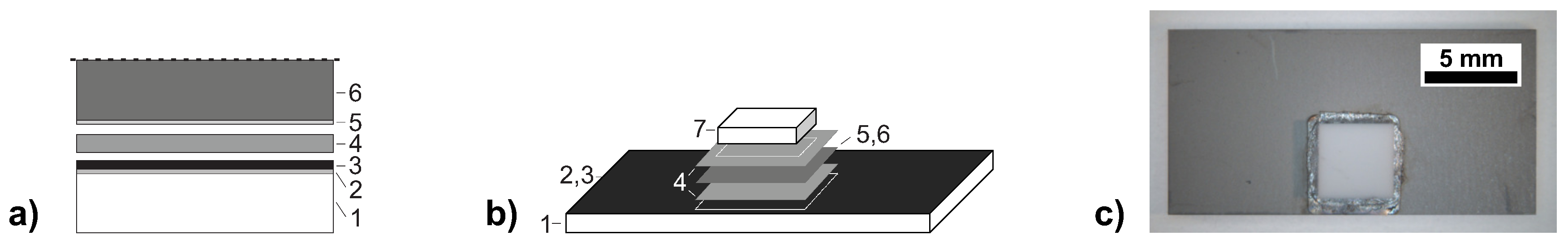
2. Materials and Methods
Reactive joining was performed with four different substrate types: (i) borosilicate glass wafers (Borofloat
®33, Schott AG, Jena, Germany) of 0.5 mm thickness, (ii) aluminium oxide (Al
2O
3) substrate plates (97% Al
2O
3, Kyocera, Kyoto, Japan) of 1 mm thickness, (iii) silicon (Si) wafers (monitor-grade mono-crystalline
-Si, Okmetic, Vantaa, Finland) of
mm thickness, and (iv) copper plates (99.95%, oxygen-free high conductivity Cu) of 1 mm thickness. The schematic joining configuration is shown in
Figure 1. In the present work, only homogeneous bonds using the same substrate materials were manufactured. The thermal properties of the different substrate types are listed in
Table 1. The substrates were metallised by magnetron sputtering with a Ni metallisation layer of 200 nm (Si) to 500 nm (rest) thickness, and with an intermediate Ti-W adhesion layer of 70 nm to 100 nm in case of Si, Al
2O
3 and borosilicate glass (in case of Cu, no adhesion layer is necessary). For the manufacturing of shear-test specimens, the substrate plates and wafers were cut into smaller plates of
(upper substrate) and
(lower substrate) using a dicing saw (Disco DAD3350).
As reactive foils, commercially available Ni(V)-Al RFs (Nanofoils
®; Indium Corporation, Clinton, NY, USA) with a thickness of 60 μm were used (For commercial production of the reactive foils by sputter deposition, instead of pure, magnetic Ni targets, non-magnetic Ni-V-targets are used in order to facilitate the sputtering process. The intermetallic phase NiAl, which is the predominant product of the self-heating reaction between Ni and Al, has a substantial solubility for V, i.e., vanadium is incorporated into NiAl, here denoted as Ni(V)Al.). The reactive foils are plated with 1 μm InCuSil
®-15 (61.5 wt% Ag, 23.5 wt% Cu, 15 wt% In; 53.3 at.% Ag, 34.5 at.% Cu, 12.2 at.% In) for oxidation protection. Pure Sn foils (97.5 at.% Sn, Goodfellow) of 10 μm thickness were used as solder. The Cu substrate plates were later galvanically pre-soldered with 12 μm (nominally 10 μm) Sn, because reactive joining with Sn foils proved to be unsuccessful (see
Section 3). The reactive foils and solder foils were cut with a laser (pulsed Nd:YAG marking laser, wave length 532
) to preforms of
(RF), respectively,
(solder foils).
The substrates and Sn solder foils were either etched with 10 % HCl and the RFs with 20 % HNO
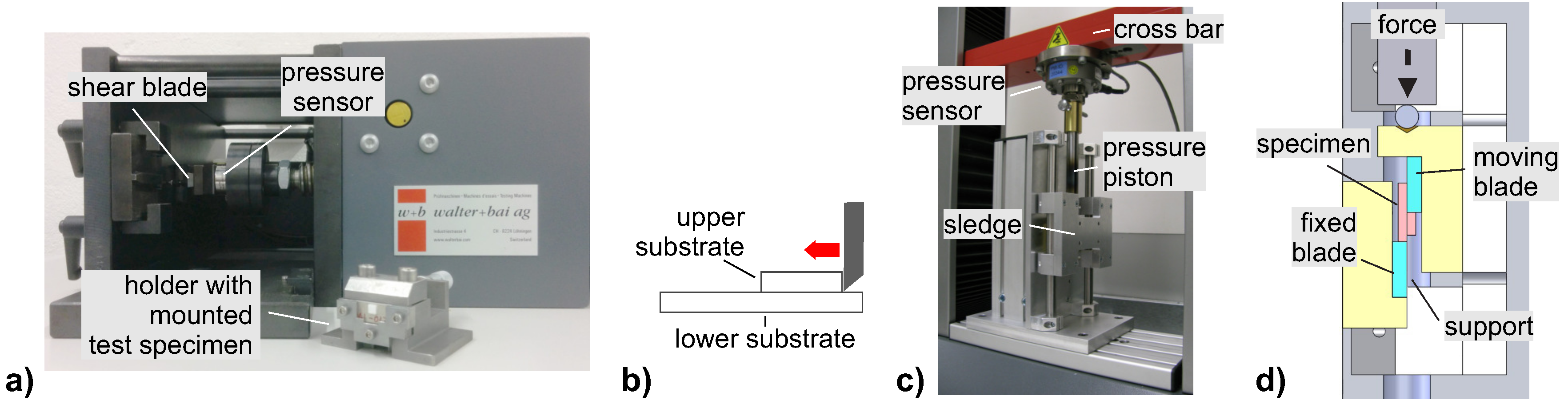
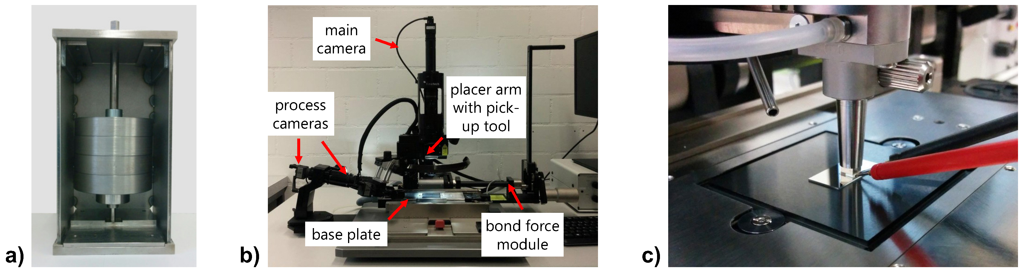
3 to reduce the amount of surface oxides, rinsed twice in demineralised water and dried with compressed air before assembly, or were only cleaned in an ultrasonic bath with isopropyl alcohol and dried. Both sample cleaning methods lead to the same performance in shear tests, indicating that etching with acids or fluxes is not mandatory. For bonding, a bond pressure of 2.5 MPa to 2.6 MPa was used. The exothermal reaction was initiated at one side of the 4 mm × 4 mm bonding area by an electrical discharge using two electrodes placed on the surface of the reactive foil with a distance of approximately 3mm. The instrumental setups used for reactive joining are shown in
Figure A1 (
Appendix A).
For investigation of the joint quality by optical microscopy (OM) and SEM, cross-sections were prepared by grinding and polishing, as well as by use of a cross-section polisher (Hitachi IM4000) for some SEM samples. OM was performed with a Leica DM6000M optical microscope, SEM-EDS was performed using a Fei NanoSem230 operated at an acceleration voltage of 10 kV (respectively 15 kV for EDS analysis). For CT, a Nikon XT V 160 Printed Circuit Board Inspection System with optional CT arm was used, operated between 127 kV to 156 kV and 13 μA to 22 μA. The shear strength of the joints was tested with a shear tester (Walter + Bay STM 20) at a constant shear rate of 0.6 mm/min, or with a tensile tester (Zwick/Roell Z010, modified for shear tests) at a constant shear rate of 1 mm/min. The devices used for performing the shear tests are shown in
Figure A2 (
Appendix A). No influence of the testing machine on the shear strength was detected.
3. Results and Discussion
Reactive joining was first performed for all four substrates using the standard joining configuration with a reactive foil of 60 μm thickness and Sn solder foils of 10 μm thickness. In this way, firm bonds were immediately obtained in case of Al
2O
3, Si, and borosilicate glass. In the latter case, the substrates showed large cracks emerging from the joining interface, which can be attributed to an overexposure to heat (i.e., thermal shock, cf. [
10]). In contrast to that, in case of Cu no bond was obtained with the standard joining configuration: although the Sn solder foils were completely melted and strongly fused to the reactive foil after the joining process, bonding of the Sn solder to the Ni-metallisation of Cu was not achieved. This difference in macroscopic joining behaviour clearly shows the effect of the different thermal conductivities of the substrate materials (see
Table 1): in case of borosilicate glass, the very low thermal conductivity of the glass leads to a heat pile-up and very high temperatures within the joining zone adjacent to the reactive foil. As a consequence of the sudden and localised heat exposure, the glass substrate experiences a thermal shock close to its surface and crack formation is initiated. Residual stresses then lead to further crack growth (this problem and its prevention is discussed in detail in [
10]). By contrast, the very high thermal conductivity in case of Cu leads to fast drainage of the heat of reaction into the substrates. As a consequence, only a temperature increase is achieved in the joining zone which is sufficient to melt the Sn shortly, but insufficient to activate the reaction of liquid Sn with the Ni surface metallisation. This problem could be solved e.g., by use of a RF with larger thickness providing more heat of reaction [
11]. The solution applied here was, for sake of comparability, to pre-solder the (Ni-coated) Cu substrates by the galvanic deposition of Sn of same thickness as the Sn-foils. This way, a direct contact between the Sn solder and the Ni metallisation is created, and it is no longer necessary to liquefy the entire solder layer completely: local melting and re-solidification of the Sn solder surface in contact with the reactive foil is enough to achieve bonding. Pre-soldering of the substrates also has the advantage that two sets of interfaces in the joining setup can be eliminated, which reduces the amount of gas trapped during joining at atmospheric pressure, i.e., the amount of porosity in the solder layers (additionally, with regard to manufacturing efficiency, two process steps for positioning of the solder foils become obsolete). Although pre-soldering of Cu with Sn may eliminate the necessity of a surface metallisation, the use of a Ni metallisation is still advised in order to prevent formation of detrimental amounts of Cu-Sn intermetallics and Kirkendall voiding during joint operation at elevated temperatures. Another feasible approach to improve the solderability with Sn solder upon reactive joining would be the use of Au as a final surface metallisation layer: Since the temperature of the Sn-rich eutectic decreases from 231 °C for the system Ni-Sn [
21] to 211 °C for the system Au-Sn [
22], a lower temperature is sufficient to generate a liquid phase at the solder-substrate interface and thus to achieve bonding.
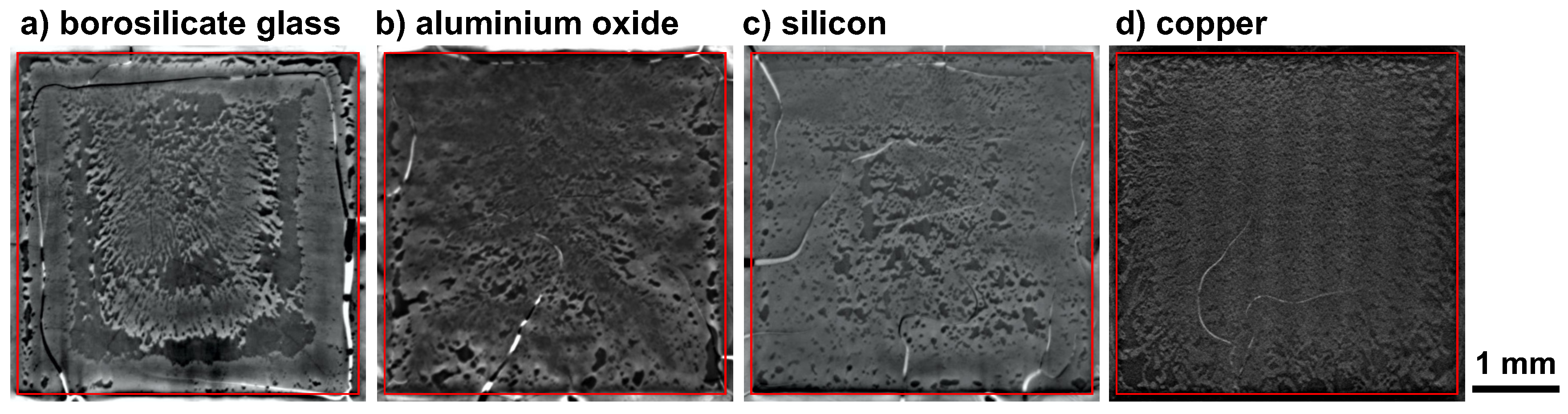
Figure 2 shows the results of the non-destructive CT tests for the upper solder layer of the different substrate types. Due to the small thickness of the solder layer, the CT slices in
Figure 2 also contain parts of the reactive foil. For all substrates, a considerable number of pores within the solder layer can be observed, as well as cracks within the reactive foil layer, which are partly filled by solder material. The cracks within the reactive foil layer are due to the pronounced volume reduction associated with the reaction of Ni and Al to NiAl, causing lateral shrinkage of the foil and formation of cracks. Cross-sectional analysis of the Sn solder foils (respectively, the Sn solder plating in case of Cu) by SEM showed a negligible amount of initial porosity in the solder before joining, i.e., the porosity predominantly originates from air enclosed within the joining setup during assembly. Although porosity is present for all substrate materials, CT shows a clear difference in the distribution of the porosity within the solder layer, resulting from the different time-temperature-profiles experienced by the joint: in case of borosilicate glass, large agglomerates of pores can be observed, while for Al
2O
3, Si and Cu, a much more homogeneous distribution of pores is present. Since the thermal conductivity defines not only the maximum temperature which is reached within the joining zone during the reaction, but also the period during which the solder is in the liquid state [
11], the solder remains liquid for a comparatively long period in case of borosilicate glass. This allows for pronounced pore condensation, i.e., coarsening of the porosity (
Figure 2a). Due to a comparatively much larger thermal conductivity in case of Al
2O
3 and Si, the solder is for a shorter time in the liquid state. As a consequence, the pore distribution is much finer (
Figure 2b,c). For Cu, the high thermal conductivity leads to rapid re-solidification of the Sn solder, and almost no coarsening of the pores can take place, leading to the very fine distribution of porosity found in the centre of the bonding area with CT (
Figure 2d).
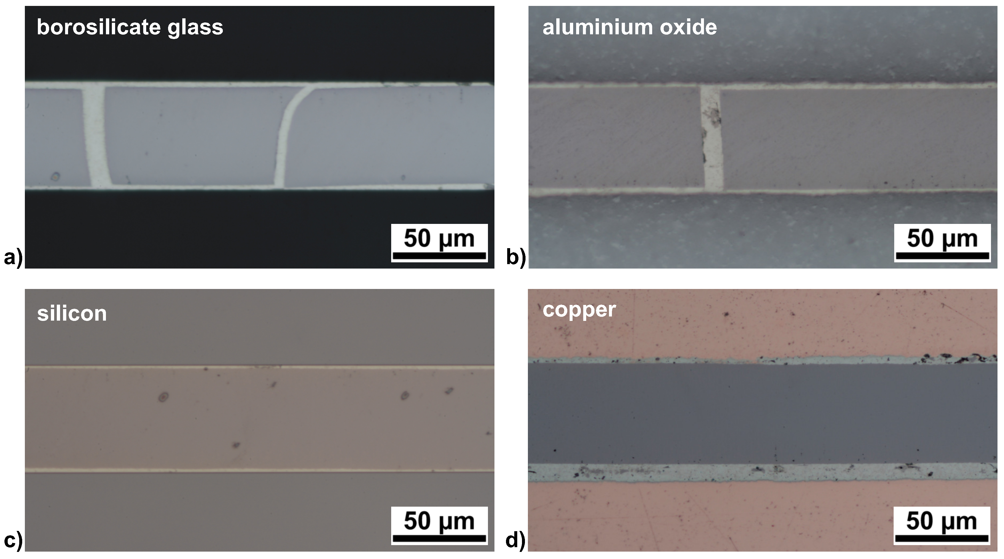
The cross-sections of the joints prepared for the four different substrate types (
Figure 3) show the typical features of solder joints prepared with reactive Ni-Al-foils: the reactive foil layer is embedded within the two solder layers and occasionally shows some cracks partly filled with solder material. Notably, the solder layers for borosilicate glass, Al
2O
3 and Si are much thinner than expected from the initial thickness of the Sn foil of 10 μm (also see
Figure 4). This shrinkage can be partly attributed to the filling of the cracks in the reactive foil layer (For some applications, the necessity to fill the cracks sets a lower limit for the thickness of the solder layer: if thinner solder layers are used, the cracks can either not be filled, which may lead to problems if e.g., a hermetic joint is required, or the remaining solder layer becomes too thin, which may lead to problems in case of components with high surface roughness and waviness.). However, the here observed shrinkage can mainly be attributed to the pronounced lateral outflow of liquid Sn out of the joining zone during the bonding step, driven by the application of the uniaxial pressure (also see [
23]). Note that this practical issue prevents modelling of the actual time-temperature-profiles as e.g., performed in [
11]: the observed lateral outflow of liquid solder leads to an undefined heat loss which makes correct modelling of the heat flow and of the corresponding time-temperature-profile impossible. For Cu, almost no shrinkage of the solder layers was observed (especially for the lower solder layer, which is in direct contact with the larger substrate acting as a large heat sink). This indicates that, during reactive joining, the Sn layers were likely not liquefied completely throughout the whole bonding area, thus preventing lateral outflow of liquid Sn under pressure. With a speed of the reaction front of approximately 8 ms
‒1 for the commercial Ni(V)-Al RFs used here (determined with a high-speed camera), the total reaction time from one side of the 4 mm × 4 mm bonding area to the other is only about 0.5 ms (also see [
23]). Hence, in case of Cu, the solder layer was in the liquid state for less than 0.5 ms, which corresponds reasonably well to model predictions for a similar scenario [
11].
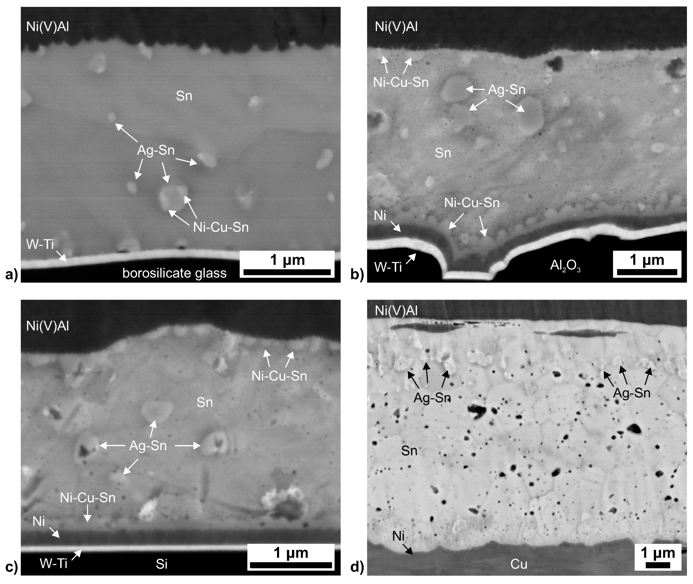
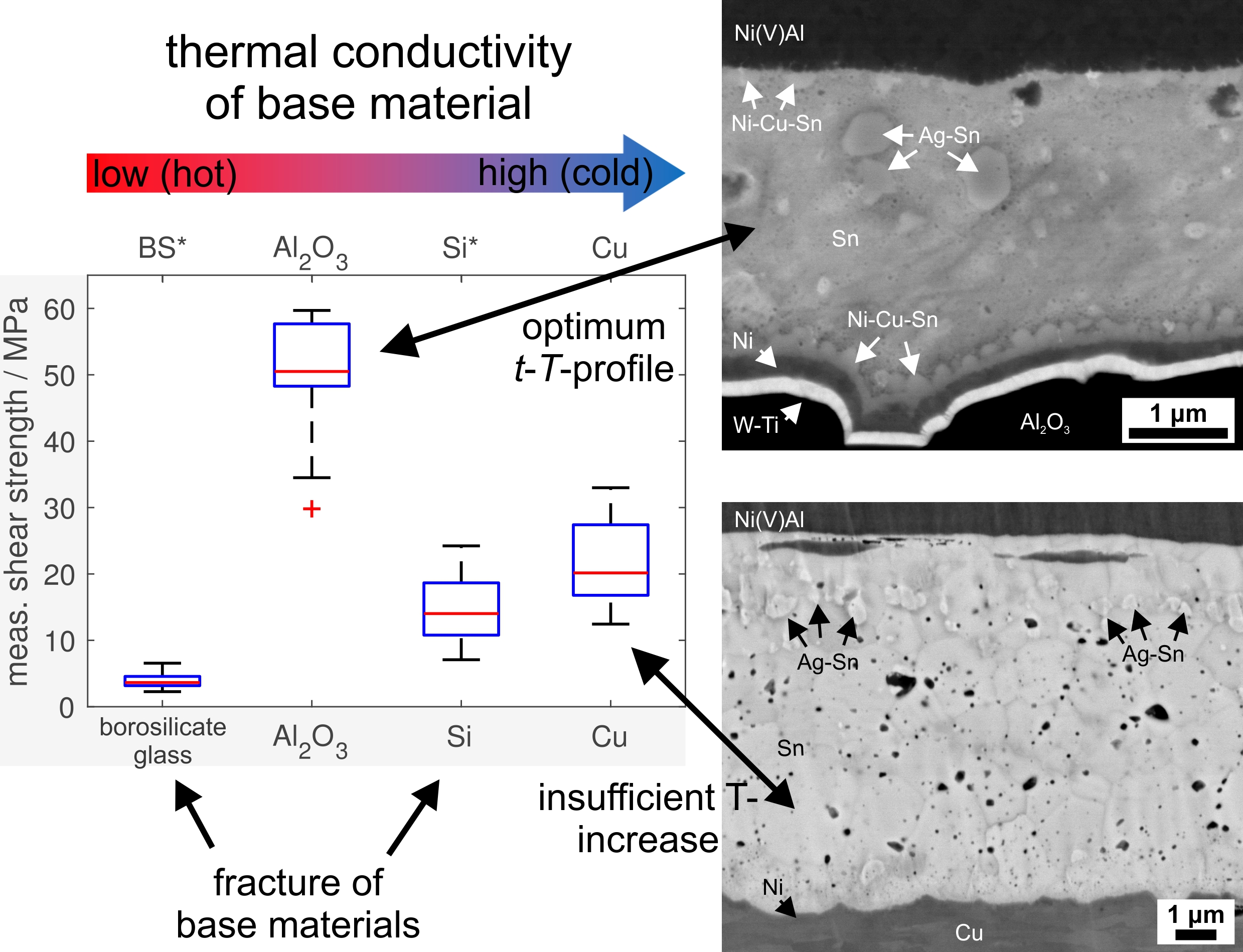
As expected, the microstructure of the joining zone resulting from the reactive bonding step is strongly affected by the different time-temperature profile evolving for the different component materials (
Figure 4): as discussed above, in case of borosilicate glass, the low thermal conductivity leads to high temperatures within the joining zone over a prolonged time. The resulting microstructure (
Figure 4a, cf. the initial setup depicted in
Figure 1) clearly shows the consequences of this extreme time-temperature profile: the Ni-metallisation of the borosilicate glass surface is completely dissolved and only the (thermodynamically very stable) Ti-W adhesion layer remains (also see [
10]). In addition, the elements of the Ag-Cu-In protection layer of the reactive foil are completely redistributed throughout the solder layer, leading to in situ alloying: the presence of Ag leads to formation of Ag-Sn intermetallic precipitates within the solder zone, most likely Ag
3Sn (cf. e.g., [
24]; note that the interaction volume of SEM-EDS is considerably larger than the size of the precipitates found in this study, which prevents the exact determination of the composition by this method). In direct vicinity of the Ag
3Sn precipitates, small particles associated with an enrichment in Ni and Cu are found, indicating the separate formation of ternary Ni-Cu-Sn intermetallic particles (most likely of the Sn-rich (Ni,Cu)
3Sn
4-phase): while a number of mixed Ni-Cu-Sn intermetallics exists in the system Ni-Cu-Sn, the mutual solubility of Ag and Ni/Cu in the respective Sn-intermetallic phases is negligible [
21,
25,
26]. For the minor alloying element In, no clear enrichments could be detected. The reactive foil layer consists of NiAl phase with some few at.% of V. Notably, at the interface between the solder layer and the reactive foil layer, pronounced scallop formation of the NiAl-phase can be observed, which is typical for the growth (and/or coarsening) of solid-phase particles in contact with a liquid phase. In case of Al
2O
3 (
Figure 4b), the Ni-metallisation layer on top of the Ti-W-adhesion layer is still intact and pronounced formation of Ni-Cu-Sn-phase scallops, probably (Ni,Cu)
3Sn
4, into the Sn-solder layer can be observed (also here, due to the smallness of the intermetallic particles with respect to the beam interaction volume, exact determination of their composition is not possible). It can thus be estimated that the temperature at the solder–metallisation interface was above the eutectic temperature of Sn-rich Ni-Cu-Sn of about 228 °C, but below the melting temperature of (Ni,Cu)
3Sn
4 of about 798 °C [
27]. Within the solder layer, again comparatively large intermetallic Ag-Sn particles can be detected, while, at the boundary between solder layer and reactive foil, formation of some Ni-Cu-Sn intermetallics can be observed. This difference in spatial distribution of the Ni-Cu-Sn and Ag-Sn intermetallic precipitates can be rationalised through the different thermodynamic behaviour of the alloy systems: in the temperature range near the respective eutectic temperature, liquid Sn has a much lower solubility for Cu and especially for Ni with respect to formation of the binary or ternary intermetallic Ni-Cu-Sn phases than for Ag with respect to formation of Ag
3Sn [
21,
25,
26]. Hence, formation of the Ni-Cu-Sn intermetallics predominantly occurs close to the Cu- and or Ni-source (i.e., the Ni-metallisation layer or the Ag-Cu-In layer) by scallop-type growth of grains into the liquid phase. By contrast, Ag can easily dissolve into the liquid Sn phase, and Ag
3Sn then only precipitates from the liquid phase at considerably lower temperatures during the cooling stage, thus forming Ag
3Sn-islands within the Sn solder layer. For Si, with a pronouncedly higher thermal conductivity than Al
2O
3 (but lower heat capacity,
Table 1), a similar microstructure is found (
Figure 4c). A marked difference is the less pronounced formation of Ni-Cu-Sn scallops along the interface between Ni-metallisation and solder layer, and an even more localised formation of Ni-Cu-Sn intermetallics along the boundary between solder layer and reactive foil, due to the shorter time at less elevated temperatures. Finally, in case of Cu, a distinctly different joint microstructure can be observed (
Figure 4d): first, along the interface between the Ni-metallisation and the Sn-solder layer, no formation of Ni-Cu-Sn intermetallic scallops takes place, although comparison with the initial microstructure of the galvanically deposited Sn-layer showed that the Sn-layer was indeed completely melted during reactive joining, i.e., temperatures of at least 232 °C were reached at the solder-substrate interface. Scallops are also absent in the transition region between the solder layer and the reactive foil layer. In addition, formation of the Ag
3Sn-phase is limited to a narrow region close to the original Ag-Cu-In-layer. Obviously, only very limited intermixing of Ag, Cu and In with the Sn-solder could take place due to the short time at comparatively low temperatures, leading to very localised precipitation of the intermetallic particles. In addition, a substantial amount of sub-micron-sized pores can be observed within the Sn-layer, in contrast to the other substrate types. This indicates that, in accordance with the results of CT (
Figure 2), only very limited coarsening of the porosity could take place in case of Cu. Hence, the microstructure developing for each joining material is strongly influenced by the thermal properties and the ensuing specific time-temperature-profile upon reactive joining.
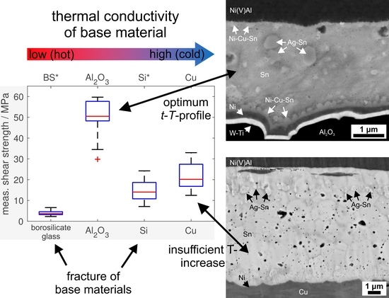
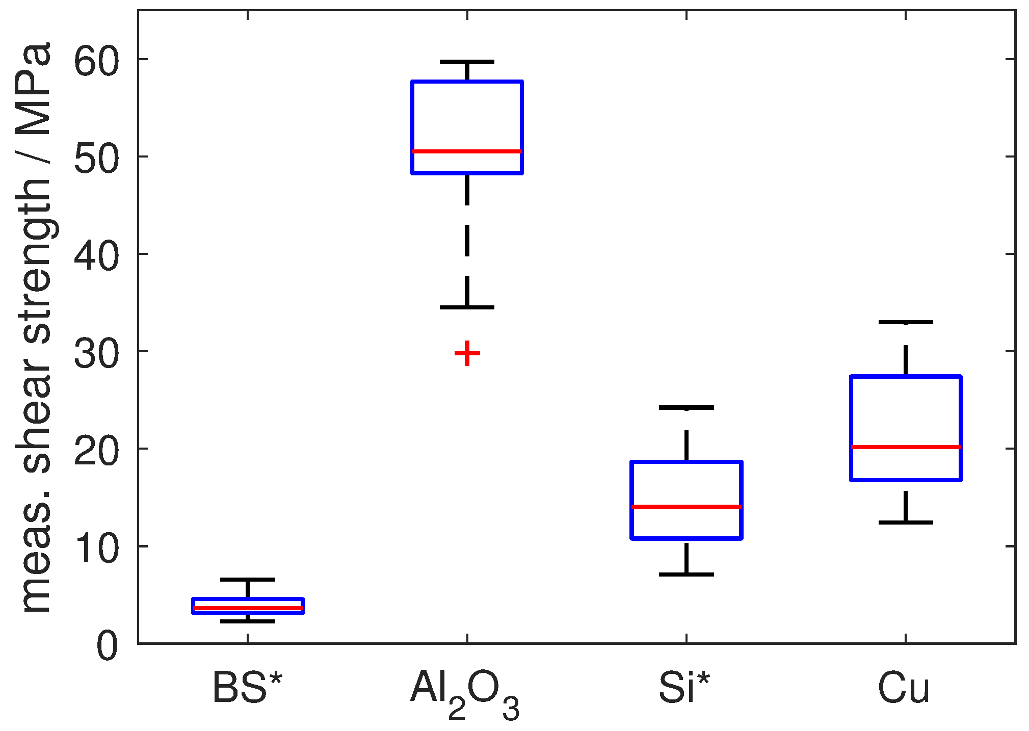
The mechanical strength of the reactive solder joints was assessed by shear tests. Although a firm bond was obtained for all four substrate types, the corresponding shear strength of the joints shows a strikingly different behaviour (
Figure 5, also see [
28]): for borosilicate glass, an apparently very low shear strength of less than 5 MPa was obtained. However, analysis of the specimens after shear testing showed that failure occurred via cracking of the substrate plates, preferentially along the cracks already formed during reactive joining and not by failure of the solder joint. Hence, this value does not represent the actual shear strength of the joint. After optimisation of the joining procedure by considerably increasing the amount of solder in order to avoid the formation of cracks, nominal shear-strength values of about 20 MPa could be obtained (see [
10]), also in this case limited by the failure of the brittle glass. For Si, the maximum shear strength was limited by brittle failure of the substrates, as well. For the mechanically more robust polycrystalline Al
2O
3, a much higher average shear strength of more than 50 MPa could be achieved (
Figure 5), with failure within the soldering zone, while, for Cu, a much lower shear strength of about 20 MPa was obtained (again with failure within the soldering zone). The observed stark discrepancy in shear strength can be explained by the peculiar microstructure formed within the soldering zone for the specific time-temperature-profile resulting from the thermal properties of the materials: in case of Al
2O
3 (and also Si), the reactive joining process leads to a joint microstructure featuring excellent mechanical properties upon shear testing: the heat generated by the reactive foil, in combination with the specific thermal conductivity of the material, is sufficient to completely liquefy the Sn solder layer and to achieve distribution of the alloying elements of the Ag-Cu-In layer throughout the solder layer. This leads to formation of intermetallics (especially Al
2O
3) evenly distributed within the solder layer. Notably, the shear strength of pure Sn solder is only about 18 MPa [
29]. Thus, the additional in situ alloying of Sn by Ag, Cu and In from the protective Ag-Cu-In layer of the RF leads to pronounced strengthening of the solder with regard to pure Sn solder. Good bonding between the solder and the metallisation layer is realised by the Ni-Cu-Sn scallop formation along the solder–metallisation interface without excessive formation of intermetallics, which would otherwise lead to embrittlement of the joint. In case of Cu, the given joining system results in a soldering profile with relatively low temperatures over a relatively short time period. As a consequence, the alloying elements Ag, Cu and In are only distributed in a small region of the Sn solder layer, which prevents an overall strengthening of the solder layer. The shear strength obtained for Cu is therefore practically identical with that of pure Sn solder (about 20 MPa vs. 18 MPa). Notably, although Cu shows the largest thermal conductivity and hence also the fastest cooling rate after foil reaction, a positive effect of microstructural refinement due to rapid quenching of the liquid solder is not observed (cf. [
1]). In order to increase the shear strength in case of the Cu substrates, instead of pure Sn a Sn-alloy solder, e.g., of the Sn-Ag-Cu-system, could be used to achieve a more homogeneous strengthening by intermetallics, albeit this may come at the price of an increase in joint brittleness due to the localised alloying effect by the Ag-Cu-In-layer of the reactive foil.
The thermal conductivity of the employed substrates or components thus has a pronounced effect on the microstructure of the joining zone obtained upon reactive joining, and accordingly also on the joint quality: the time-temperature-profile developing within the joining zone as a function of the thermal conductivity defines the formation, amount and spatial distribution of intermetallics within the joining zone, which again define the mechanical performance of the joint. Optimum reactive joining finally requires adjustment of two factors: first, balancing of heat production and heat dissipation (for given joining components conveniently done by adjustment of RF type and thickness), and second, careful adjustment of the joining system by deliberate selection of solder type and thickness, surface metallisations and RF coatings for in situ alloy formation. In particular, the in situ alloying, here observed for the Cu-Ag-In-coating of the commercial RFs, presents a promising route to tailor the joint microstructure for optimum performance.

 ,
, 


