Abstract
As the interconnect delay exceeds the gate delay, the integrated circuit (IC) technology has evolved from a transistor-centric era to an interconnect-centric era. Conventional metallic interconnects face several serious challenges in aspects of performance and reliability. To address these issues, nanocarbon materials, including carbon nanotube (CNT) and graphene, have been proposed as promising candidates for interconnect applications. Considering the rapid development of nanocarbon interconnects, this paper is dedicated to providing a mini-review on our previous work and on related research in this field.
1. Introduction
The breakthrough development of the semiconductor industry has revolutionized human society, from personal electronic gadgets, commercial and industrial equipment to military and aeronautical facilities. As predicted by Moore’s law, the number of transistors within a chip doubles about every two years, while the cost comes down [1]. According to the International Technology Roadmap for Semiconductors (ITRS) projection, a 10 nm minimum feature size could support a tera-scale chip with a trillion transistors by 2020 [2]. Such phenomenal progress has been achieved through scaling of digital integrated circuit (IC) feature size to smaller physical dimensions.
The ongoing miniaturization of the IC feature size has had a significant benefit in increasing the transistor speed. However, different from the transistor, the interconnect performance would be degraded due to the reduced conduction area and increased scattering probability for electrons [3,4]. Under such circumstances, the chip performance is restricted by the shrinking interconnect dimensions on account of both the interconnect delay and the power dissipation. Moreover, the interconnect reliability has been becoming a more and more important problem, as the ampacity of conventional Cu wire cannot satisfy the increasingly stringent requirements [2,5,6]. Therefore, interconnects have become the major challenge in the design of modern ICs, thereby leading to the transition of IC technology from transistor-centric to interconnect-centric [7]. To address the interconnect challenges for next-generation ICs, diverse improvements of interconnect optimization and design methods have been reported, such as a low-k dielectric structure, three-dimensional integration, and inter-chip optical interconnects [8,9,10].
Nanocarbon materials have attracted much attention since the carbon nanotube (CNT) was discovered by an arc-discharge evaporation method in 1991 [11]. Graphene, a Nobel Prize honored discovery, has further promoted the research in this field [12]. It was found that nanocarbon materials have many extraordinary physical properties. For example, the ultrahigh thermal conductivity of nanocarbon materials can help heat dissipation in high-density integrated systems [13,14,15]. The maximum current-carrying density of a CNT is more than two orders higher than that of Cu wires, thereby mitigating the electromigration-induced reliability problems [16]. It is natural to apply nanocarbon materials as an alternative option to potentially replace Cu for interconnects and passive devices in ICs [17,18,19,20,21,22]. In recent years, there have been many publications in the literature devoted to the design, modeling/analysis, and fabrication/integration of nanocarbon interconnects. This paper seeks to review recent research efforts and progress in the nanocarbon interconnects. In particular, this paper focuses on the modeling and direct current (DC) performance analysis of nanocarbon interconnects for next-generation digital ICs.
2. Graphene Nanoribbon (GNR) Interconnects
Physically, graphene is a 2D monolayer of carbon atoms packed into a honeycomb lattice, and the quasi-1D graphene nanoribbon (GNR), as shown in Figure 1a, can be utilized as on-chip interconnects [23]. Depending on the edge shape, a GNR can be zigzag, armchair, or chiral (other shapes). The zigzag GNR is always metallic, whereas the armchair GNR is metallic or semiconducting, depending on the number of carbon atoms across its width. Different from the GNR, a CNT’s chirality is defined by its circumferential edge shape. A single-walled carbon nanotube (SWCNT) can be visualized as a seamlessly rolled-up GNR, on the basis of which a novel fabrication method has been developed to unzip the CNT to form a GNR [24]. A multi-walled carbon nanotube (MWCNT) is a parallel assembly of coaxial SWCNTs, and the neighboring shells in an MWCNT are separated by the van der Waals gap.
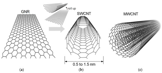
Figure 1.
Schematics of (a) monolayer graphene nanoribbon (GNR), (b) single-walled carbon nanotube (SWCNT), and (c) multi-walled carbon nanotube (MWCNT).
2.1. Multilayer Graphene Nanoribbon (MLGNR) Interconnects
In comparison to the CNT, the GNR can be easily controlled horizontally and is more compatible with conventional lithography [24]. By using the tight-binding approximation, the conductance of a monolayer GNR has been calculated as a function of width , Fermi level , and specularity parameter for edge diffuse scattering in Reference [25]. It was demonstrated that the atomically thick monolayer GNR could outperform Cu wire for widths below 8 nm. Figure 2a shows the schematic diagram of a monolayer GNR interconnect with its equivalent circuit model. In the model, is the contact resistance, and it can be calculated by:
where is the imperfect contact resistance, and it highly depends on the fabrication technology. is the quantum contact resistance, and it is calculated as , where is the Planck’s constant and is the electron charge. The number of conducting channels in a monolayer GNR can be calculated by [26,27]:
where is the Boltzmann’s constant and is the temperature. For a given width of the metallic armchair GNR with and , can be approximated as , where and are in units of nanometers and electron volts, respectively [28]. The total resistance of a monolayer GNR is given by:
where is the interconnect length, and is the effective MFP (mean free path) for the ith subband. The MFP is determined by various scattering mechanisms, and it is a function of the specularity parameter [29]. Herein, the fully diffusive GNR can be represented by , meanwhile, represents that the GNR is fully specular.
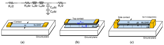
Figure 2.
Schematics of (a) monolayer GNR interconnect, (b) top-contacted MLGNR, and (c) side-contacted MLGNR interconnect.
However, it is worth noting that the physical properties of monolayer GNR is susceptible to the substrate influence, which can be avoided for the case of multilayer GNR (MLGNR). Moreover, MLGNR has superior characteristics for signal propagation as the multilayer structure can effectively reduce the interconnect resistance [29,30,31,32]. Figure 2b,c show the schematic diagrams of MLGNR interconnects with top contacts and side contacts, respectively. In the figure, denotes the van der Waal’s gap between the adjacent graphene layers, is the thickness of the MLGNR interconnect, and the number of graphene layers , where “” represents that only the integer part is considered.
To date, most of the experiments on multilayer graphene have employed top contacts, as shown in Figure 2b [33,34,35]. For the top-contacted MLGNR interconnect, Kumar, et al. [36] developed a resistor circuit model with the consideration of in-plane resistance and perpendicular resistance between adjacent layers . It was found that the perpendicular resistance makes the conductance a nonlinear function of the number of graphene layers. Further, Pan, et al. [37] conducted a benchmark study, which indicated such top-contacted MLGNR can exhibit advantages under certain circumstances. With the increasing interconnect length, however, the in-plane resistance increases, while the perpendicular resistance decreases continually. It can be seen in Figure 3, that as the length exceeds a certain value, the influences of the contact type and interlayer coupling can be ignored, and the top-contacted MLGNR can be treated as a side-contacted one [28].
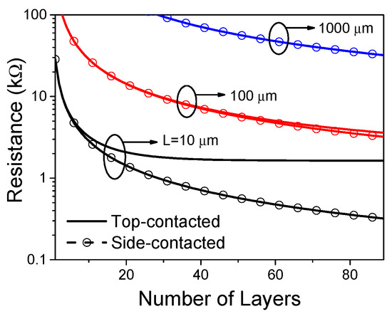
Figure 3.
Effective resistances of top-contacted and side-contacted MLGNR interconnects with Fermi level , specularity parameter , and c-axis resistivity [28].
Figure 4 shows the multi-conductor transmission line model and the simplified equivalent single-conductor (ESC) transmission line model of a side-contacted MLGNR interconnect. In the multi-conductor model, the mutual capacitance and inductance between the adjacent graphene layers have been considered. The MLGNR interconnects are assumed to be decoupled, because several decoupled graphene layers have been grown experimentally in References [33,34], and demonstrated theoretically in Reference [39]. In this case, the resistance of the MLGNR interconnect is a parallel connection of the resistance of each layer, i.e., . The per-unit-length (p.u.l.) magnetic inductance and electrostatic capacitance are determined by the MLGNR geometry and its surrounding dielectrics. By applying the boundary conditions, the equivalent kinetic inductance and quantum capacitance in the ESC model can be obtained by recursive schemes [40,41]. As the kinetic inductance is much larger than the magnetic inductance, the equivalent kinetic inductance in the ESC model can be expressed as [28]:
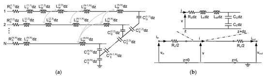
Figure 4.
(a) Multi-conductor transmission line model and (b) equivalent single-conductor (ESC) transmission line model of side-contacted MLGNR interconnect [38].
The equivalent quantum capacitance is mainly determined by the mutual coupling one between the adjacent layers. As the number of layers is larger than eight, the equivalent quantum capacitance can be given by:
Based on the extracted parameters, the 50% propagation delay can be calculated by [42]:
where is the driver resistance, is the load capacitance, , , and
Due to large driver resistance, nanocarbon interconnects will not exhibit superior performance compared to conventional Cu wires at the local level. So our attention is focused on the intermediate level and global level MLGNR interconnects. Figure 5 shows the time delay ratios of MLGNR and Cu wires at the intermediate level and global level, respectively. The inverter size is assumed as 50 and 100 times larger than the minimum-sized gate, respectively, at these levels. The imperfect contact resistance is neglected, and the Fermi level is set as 0.6 eV. As shown in Figure 5, the MLGNR interconnects with fully specular edges show superior performance over Cu wires at both the intermediate and global levels. Such an advantage can be enhanced with the feature size scaling down. However, when the specularity parameter decreases to 0.8, the electrical performance of the MLGNR interconnects will degrade to the comparable level of Cu wires. Therefore, it can be concluded that the MLGNR interconnects have the potential to outperform conventional Cu wires at an advanced technology node, and more attention should be paid to the edge quality.
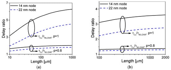
Figure 5.
Time delay ratios of MLGNR interconnects and Cu wires at the (a) intermediate level and (b) global level [28].
2.2. Vertical Graphene Nanoribbon (VGNR) Interconnects
Although the MLGNR interconnects show excellent electrical properties in terms of low resistance and high reliability, they may hinder the heat dissipation in vertical direction due to the anisotropic property [43]. To resolve this issue, the scheme of vertical graphene nanoribbon (VGNR) interconnect, as shown in Figure 6, was proposed and studied in [44]. Unlike the top-contacted MLGNR interconnect shown in Figure 2b, each layer in VGNR interconnect can participate in the electron transport, thereby reducing the contact resistance.
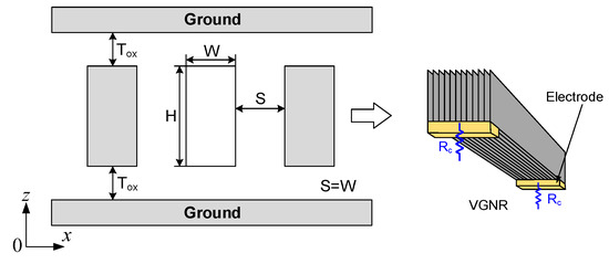
Figure 6.
Schematic of vertical graphene nanoribbon (VGNR) interconnect.
As described in [45], the vertical graphene layers have been realized experimentally. Definitely, further improvement in the fabrication of long and highly aligned VGNRs is still required for their practical usage as on-chip interconnects [46]. A possible fabrication process is outlined briefly in the following. First, a catalyst layer is sputtered to grow graphene layers. Then, the vertical graphene layers grow below these layers, which are removed subsequently. VGNR interconnects are obtained finally by patterning the vertical graphene layers. As aforementioned, VGNRs can also be assumed to be decoupled [33,34,39], and the resistance is a parallel connection of the resistance of each layer.
Figure 7a shows the p.u.l. resistance of a monolayer GNR interconnect with a 400 µm length and the 0.2 eV Fermi level. It is shown that the resistance of a monolayer GNR increases with the decreasing width. For GNRs with , the resistance increases superlinearly with the decreasing width when the width becomes smaller than 10 nm. This superlinear relationship between GNR resistance and width becomes more significant as decreases. Note that for on-chip interconnect applications, the aspect ratio is always larger than 1 [2]. Therefore, it can be concluded that VGNR, which has a larger GNR width, possesses smaller resistivity than horizontal MLGNR. Figure 7b shows the time delay of Cu, horizontal MLGNR, and VGNR interconnects at the intermediate level. It can be found that the decrease in specularity parameter can effectively improve the electrical performances of GNR interconnects. When , the horizontal MLGNR and VGNR show similar performances. As is well known, however, the perfectly specular edges are difficult to fabricate [47]. Therefore, in practical applications, for , the VGNR interconnect can provide smaller time delay than horizontal MLGNR interconnect. In other words, VGNR interconnect requires smaller specularity parameter than the horizontal MLGNR one, thereby reducing the process difficulty.
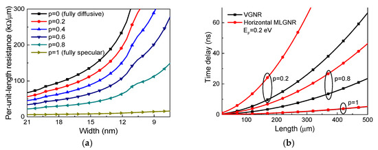
Figure 7.
(a) Per-unit-length resistance of the monolayer GNR with different specularity parameters. (b) Propagation delay of intermediate level Cu, horizontal MLGNR, and VGNR interconnects at the 7.5 nm technology node [44].
As described earlier, the graphene is an anisotropic material, and its out-plane thermal conductivity is much lower than the in-plane one. Here, the in-plane and out-plane thermal conductivities of graphene are assumed as 1750 W/m·K and 10 W/m·K, respectively [48]. Under such circumstance, the horizontal MLGNR would hinder heat dissipation in vertical direction, thereby threatening the IC performance and reliability. It has been found that VGNR interconnects are likely to solve this problem. Figure 8a depicts the unit cell for simulation performed in commercial software COMSOL Multiphysics, with the geometrical parameters adopted at the 7.5 nm technology node from ITRS projection [2]. In the simulation, an equivalent packaging layer is considered, and the bottom junction temperature and the top ambient temperature are assumed as 378 K and 318 K, respectively. By injecting power into the topmost global interconnect, the temperature rise as a function of input power can be depicted as shown in Figure 8b and the plots the temperature profiles could be obtained as shown in Figure 8c. It is evident that the heat dissipation problems, which is crucial for future nanoscale ICs development, can be effectively avoided by VGNR interconnects [49].
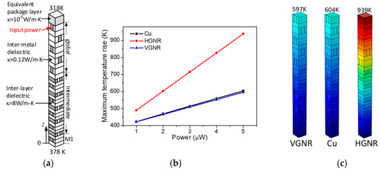
Figure 8.
(a) Unit cell for simulation. (b) Maximum temperature rise on interconnects versus input power. (c) Temperature profiles of the unit cell with a power of 5 µW input at the topmost global interconnect [44].
3. CNT Interconnects
Similar with GNR, CNT possesses long MFP, high ampacity, and large thermal conductivity [14,16,50,51,52]. Based on the Luttinger liquid theory, Burke firstly developed the transmission line model of a metallic SWCNT interconnect [53]. The equivalent circuit model of an isolated SWCNT interconnect is the same as the circuit model shown in Figure 2a, with the CNT diameter denoted as . The number of conducting channels of a metallic SWCNT is 2, and the MFP is usually 1000. Although an SWCNT possesses many unit properties and some efforts have been devoted to reducing the SWCNT resistance by doping, an isolated SWCNT is still too resistive for interconnect applications in high-performance ICs [54,55]. It can only be used in some specific applications such as subthreshold circuits and sub-10 nm circuits [56,57,58]. To reduce the CNT resistance, three kinds of CNT interconnects, i.e., monolayer SWCNT, bundled SWCNT, and MWCNT interconnects, have been widely studied, as shown in Figure 9.
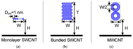
Figure 9.
Cross-sectional views of (a) monolayer SWCNT, (b) bundled SWCNT, and (c) MWCNT interconnects.
As discussed in [59], for short local interconnects, the interconnect resistances are not important, while their capacitances play a key role. So the electrical performance can be improved by using low aspect ratio interconnects such as monolayer metallic SWCNT. It can be seen in Figure 10a that monolayer SWCNT interconnect possesses smaller parasitic capacitance than Cu wire. Therefore, it can be expected that monolayer SWCNT interconnects can reduce power dissipation and crosstalk noise [60]. Figure 10b depicts the energy-delay product (EDP) ratio between Cu wire and monolayer SWCNT interconnect. Here, the imperfect contact resistance is neglected as it is highly dependent on the process. As the length exceeds 20 µm, the EDP ratio becomes larger than 1, indicating that the monolayer SWCNT interconnect can provide better performance than the Cu counterpart. Moreover, the advantage of monolayer SWCNT interconnect becomes more evident for smaller inverter size.
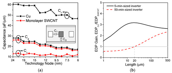
Figure 10.
(a) Parasitic capacitances of Cu and monolayer SWCNT interconnects. (b) Energy-delay product ratio between Cu and monolayer SWCNT interconnects at the 19 nm technology node [60].
To further reduce the interconnect resistance, as shown in Figure 9b, the bundled SWCNTs have been proposed and manufactured [61,62,63]. It is worth noting that for the pristine SWCNTs with random distribution of chirality, one-third are metallic and two-thirds are semiconducting. Researchers have been continually tasked to improve the metallic fraction. For instance, Harutyunyan, et al. [64] successfully fabricated a bundled SWCNTs with very high metallic fraction of 0.91. Based on physical models, Naeemi, et al. [65] developed the circuit model for bundled SWCNT interconnect and demonstrated its potential for solving several major challenges facing gigascale integrated systems. Besides the applications as horizontal interconnects, bundled SWCNTs were also proposed as on-chip vias to reduce temperature rise and increase the electromigration resistance [66,67,68,69].
Unlike SWCNTs, MWCNTs are always metallic. By assuming one-third of shells are metallic, the number of conducting channels of a shell in an MWCNT can be calculated by [70]
where . For an MWCNT interconnect, as shown in Figure 9c, it is usually assumed that the innermost shell diameter is half of the outermost shell diameter, and the aspect ratio is 2, i.e., two parallel MWCNTs are stacked. In general, an MWCNT possesses a longer MFP but smaller number of conducting channels than the bundled SWCNTs with the same cross-sectional dimensions. For MWCNT interconnects, Li, et al. [71] developed a multiconductor transmission line model, which was further simplified as an ESC transmission line model [40]. It was demonstrated that the ESC model can accurately predict the time delay and facilitate the simulation speed although it would result in an overestimation of peak crosstalk [72]. Based on the ESC model, Liang, et al. [73] characterized the performance of MWCNT interconnects by using the finite-difference time-domain (FDTD) method. Further, some studies have been conducted to analyze the crosstalk, variability, Joule heating, and electrostatic discharge (ESD) reliability of CNT interconnects [64,74,75,76,77,78,79,80,81,82,83].
On the other hand, to reduce the interconnect delay, the repeater insertion is usually employed in the design of high-performance VLSI [42]. Previous studies have been carried out to investigate the optimal repeater insertion for CNT interconnects [75,84]. Unfortunately, these studies didn’t consider the impact of metal-CNT contact resistance, which would be added along with each inserted repeater and surely influence the time delay, as shown in Figure 11 [85]. To resolve this issue, an analytical expression of the optimal repeater number was derived based on the Elmore delay equation in [86]. Furthermore, the influence of inductance on the repeater design in an MWCNT interconnect was considered [87]. Using the multivariable curve fitting technique, the closed-form expressions of optimal repeater size and the optimal number of segments can be obtained. Definitely, the smaller contact resistance is, the better performance can be achieved. Here, the maximum tolerant contact resistance of MWCNT interconnect is defined, beyond which the total time delay of MWCNT interconnect would be larger than that of Cu counterpart. Figure 12 gives the minimum time delay of an MWCNT interconnect versus contact resistance. It is shown that the maximum tolerant contact resistance increases from 3.3 kΩ to 10.5 kΩ as the technology node scales from 14 nm to 7 nm. Considering the size effect, however, the contact resistance will be scaled up 4 times from 14 nm node to 7 nm node. In other words, more efforts should be put on reducing the contact resistance with the technology advanced.
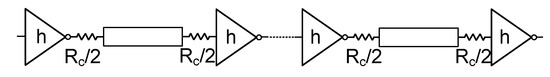
Figure 11.
Repeater insertion in a long global nanocarbon interconnects.
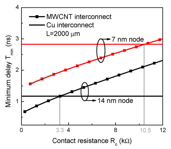
Figure 12.
Minimum time delay versus contact resistance for 2000 μm-long Cu and MWCNT interconnects [87].
As the IC feature size scales down, interconnects consume more and more power. Simply ignoring the power consumed by repeaters would cause an overestimation of optimal repeater number. Therefore, some repeater insertion methodologies have been developed targeting in reducing power dissipation of conventional Cu interconnects [88,89]. Further, a repeater design methodology to reduce delay and power of CNT interconnects has been proposed in [90], with the metal-CNT contact resistance treated appropriately. In [90], the particle swarm optimization (PSO) algorithm was employed to capture the optimal values of repeater size and repeater number. To facilitate the simulation speed, the obtained data was then used to train a neural network, as shown in Figure 13a. It was demonstrated that the trained neural network can predict the optimal repeater size and number rapidly and accurately, as shown in Figure 13b.
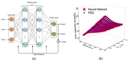
Figure 13.
(a) Schematic of the back propagation neural network. (b) Optimal repeater size of MWCNT interconnects obtained using the PSO algorithm and trained neural network [90].
4. All-Carbon 3-D Interconnects
In general, CNTs grow vertically, whereas graphene is formed horizontally. So, it is natural to develop the 3-D interconnects by combining vertical CNT vias and horizontal GNR interconnects, as shown in Figure 14. Nihei, et al. [91] firstly conceived, designed and realized the experiment to grow an MWCNT via on multilayer graphene. The critical issue to fabricate such “all-carbon” 3-D interconnects is to achieve a low electrical contact between the CNT via and the GNR interconnect. Further, Ramos, et al. [92] introduced a process to selectively grow CNTs on monolayer graphene. They demonstrated that the growth of CNTs would not damage the integrity of graphene and characterized the contact resistance between CNTs and graphene. Zhou, et al. [93] studied the CNT-graphene interface using transmission electron microscope and found that C-C bonding exists between CNT and graphene. Recently, Jiang, et al. [94] comprehensively investigated the fabrication, integration, and reliability of such “all-carbon” 3-D interconnects. Besides, it is worth noting that another “all-carbon” 3-D interconnect scheme, i.e., a dense vertical and horizontal graphene structure, has been demonstrated in [91].
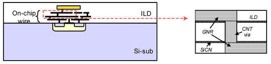
Figure 14.
Schematic of all-carbon 3-D interconnect.
Using the finite-element method (FEM), the electrothermal characteristics of all-carbon 3-D interconnects have been studied in [95]. Figure 15a shows the simulation model, which is formed by one horizontal interconnect and two vertical vias. The 3-D interconnect structure is embedded into an interlayer dielectric, whose thermal conductivity is about 0.12 W/m·K. The bottom temperature is assumed as 363 K, and the other boundaries are set as adiabatic. The out-plane electrical conductivity of the MLGNR is 1 S/m. The geometrical parameters are adopted at the 22 nm technology node from the ITRS projection [2]. With a current of 0.4 mA injected, the temperature profiles are plotted in Figure 15b–d. In the simulation, a 1 nm-thick thin plate was used to capture the influences of contact resistance. Due to the impact of quantum contact resistance, all-carbon 3-D interconnect is more resistive than Cu counterpart, thereby increasing the temperature rise. On the contrary, the CNT vias help heat dissipation from hotspots to the bottom layer. Therefore, the maximum temperature is slightly increased with the implementation of all-carbon 3-D interconnects. The results also imply that CNT vias are more suitable to be placed near bottom layer.
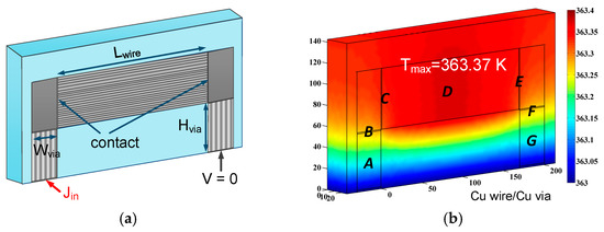
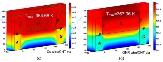
Figure 15.
(a) Schematic of a simulation model. (b–d) Temperature profiles of Cu, SWCNT vias/Cu wire, and SWCNT/MLG interconnects [95].
5. Cu-Nanocarbon Interconnect
5.1. Cu-Graphene Interconnect
During the past decades, tremendous progress has been made in the fabrication/integration of nanocarbon interconnects. However, the gap between theoretical studies and practical applications still exists. For example, the assumption of closed packed CNTs is invalid as the density of CNTs still cannot satisfy the requirements [96]. Also, the application of MLGNR interconnects encounters a serious challenge, i.e., graphene tends to behave more like graphite as the number of graphene layers increases [97]. In this perspective, Cu/low-k interconnect may be still a good choice for next-generation ICs [98].
In the application of Cu/low-k interconnect, a highly resistive diffusion barrier layer is required to prevent the diffusion of copper atoms into substrate. This barrier layer would occupy a certain area, thereby decreasing the conduction area of interconnects and increasing the effective resistivity. More importantly, the barrier layer thickness cannot scale as rapidly as the interconnect dimensions [4]. This problem becomes more and more serious with the technology advanced. To resolve this problem, graphene, the thinnest 2-D material in nature, has been proposed as the ultimate barrier layer [99,100,101]. It has been demonstrated that graphene barrier layer can help improving the breakdown current density, enhancing the electromigration lifetime, increasing the Cu grain size, and reducing the scattering probability at the surface [102,103,104,105,106]. Moreover, low-temperature deposition techniques for producing graphene on Cu and dielectric implies that the fabrication of graphene barrier layer can be compatible with traditional CMOS technology [101,104,107,108].
Figure 16 shows the schematic view of a Cu-graphene interconnect, i.e., Cu wire encapsulated with graphene barrier layers. To gain an in-depth understanding of such a Cu-graphene interconnect, it is necessary to develop its circuit model and evaluate its electrical and thermal performances. In [109], a distributed resistor model for Cu-graphene interconnect has been established, and the Cu-graphene interface resistance and graphene-graphene interface resistance have been considered and treated appropriately. The effective resistance of Cu-graphene interconnect can be derived as
where represents the number of segments meshed along the interconnect length, is the resistance of the central Cu wire, is the unit diagonal matrix, and can be obtained using the Kirchhoff’s voltage law. The subscripts , , , and represent the respective corresponding quantities as graphene barrier layers are placed at the top, bottom, left, and right surfaces of the Cu wire. It was demonstrated that the graphene barrier layers can share part of the current, thereby reducing the current passing through the central Cu wire and improving the reliability. Moreover, as the interconnect length exceeds several tens of micrometers, the central Cu wire, and graphene barrier layers can be treated as being parallel connected, and the effective resistance can be simplified as , where denotes the resistance of graphene barrier layer and is the layer number [110].
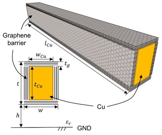
Figure 16.
Schematic of Cu-graphene interconnect.
Figure 17a depicts the effective resistivity of Cu-graphene interconnects versus temperature. According to ITRS prediction, the barrier layer thickness would scale down to 1.3 nm at the 22 nm node [2]. However, such prediction is too optimistic and too challenging. Here, the barrier layer thicknesses of 1.3 nm and 2 × 1.3 nm are considered as references. It is evident that the effective resistivity can be reduced significantly by introducing graphene barrier layer, which is mainly due to the reduced Cu surface scattering [104]. Further, Figure 17b compares the effective resistivity of Cu wire and Cu-graphene interconnect at different technology nodes. The barrier layer thickness at each node is adopted from the ITRS projection [2]. It was found that the advantage of Cu-graphene interconnect over Cu wire becomes more significant with the IC feature size scaling down.
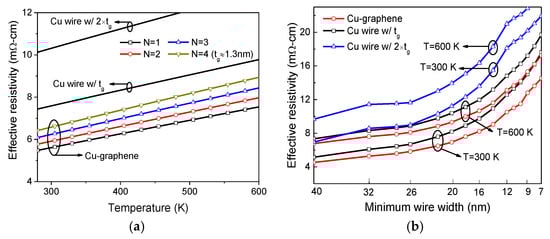
Figure 17.
Effective resistivity of Cu and Cu-graphene interconnects versus (a) temperature and (b) technology node [110].
5.2. Cu-CNT Composite Interconnect
Generally speaking, nanocarbon and conventional metals have their own pros and cons for interconnect applications. For instance, nanocarbon has high ampacity, but their conductivity is still low due to fabrication limits. On the contrary, the fabrication and integration processes of metal interconnects are mature, but the ampacity of metals cannot satisfy the requirements [2]. Subramaniam, et al. [111] attempted to advance a possible solution to this problem by co-depositing Cu with CNTs, i.e., Cu-CNT composite interconnect. It was experimentally demonstrated that Cu-CNT composite interconnect can achieve a balance between performance and reliability. This is, such Cu-CNT composite interconnect possesses a 100 times higher ampacity, but comparable conductivity than the Cu counterpart. The presence of CNTs inside Cu wire can also alleviate the electromigration void growth rate by about four times, which is due to large Lorenz number of the CNTs [112,113].
Figure 18 shows the schematic of a Cu-CNT composite interconnect over a ground plane. In the figure, identical CNTs are uniformly distributed inside the Cu wire. The CNTs can be SWCNTs or MWCNTs. Here, we define the CNT filling ratio as , where 0.31 nm is due to the separation between carbon and Cu atoms. The p.u.l. scattering resistance of the Cu-CNT composite interconnect can be calculated as , where [114,115]. The effective conductivity of CNTs is given by [116]
where Fm the metallic fraction, and ZCNT is the self-impedance of an isolated CNT.
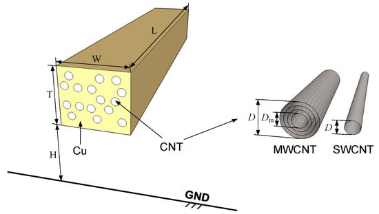
Figure 18.
Schematic of Cu-CNT composite interconnect.
Figure 19a compares the effective resistivities of Cu, SWCNT, and Cu-SWCNT composite interconnects. Unlike the ideally packed SWCNTs discussed earlier, it is assumed that the CNT filling ratios are 0.3, 0.45, and 0.6 in the figure. It is evident that the resistivity of such sparsely distributed SWCNTs is much larger than Cu counterpart. However, co-depositing Cu with such sparsely distributed SWCNTs can reduce the resistivity. The predicted values are close to the measured data, which ranges from 2 to 2.27 µΩ [111]. Further, the time delays of Cu, SWCNT, and Cu-SWCNT composite interconnects are plotted in Figure 19b. The Cu-SWCNT composite interconnect can provide comparable performance with Cu counterpart, while the sparsely distributed SWCNTs show much worse performance due to their large resistivity. As the CNT quality may be degraded due to fabrication limits, the cases of lower value of CNT MFP are also plotted in Figure 19b. It can be seen that the Cu-SWCNT composite interconnects are much less influenced than pure SWCNTs.
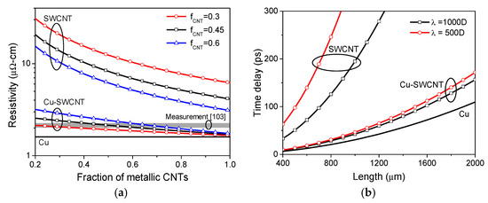
Figure 19.
(a) Effective resistivity and (b) time delay of Cu, SWCNT, and Cu-SWCNT composite interconnect [114].
In summary, this paper reviewed the current status of research on nanocarbon interconnects from the modeling perspective. The electrical performances of GNR, CNT, and Cu-nanocarbon interconnects are analyzed and discussed, with their pros and cons illustrated in Table 1. Although Cu wires have been widely used in modern ICs, their resistivity increases significantly with the scaling of feature size, which is exacerbated by the influence of diffusion barrier layer. In comparison with Cu counterparts, nanocarbon interconnects including GNR and CNT possess long MFP, high ampacity, and high electromigration resistance. However, the electrical properties of horizontal graphene are susceptible to substrate. Moreover, as nanocarbons are anisotropic, both MLGNR and CNT interconnects would hinder the IC heat dissipation. This problem can be resolved by utilizing VGNR interconnects although there is still a long way to go in the fabrication methods.

Table 1.
Comparison of Cu, GNR, CNT, Cu-graphene, and Cu-CNT interconnects.
Graphene was recently proposed as the ultimate diffusion barrier layer for Cu interconnect technology. By coating graphene onto Cu wires, the surface scattering of electrons in Cu can be reduced, and the grain size can be increased. To maximize the effective conduction area, large grain single-layer graphene is desired, and more efforts should be devoted to the development of low temperature and transfer free graphene growth techniques on dielectric and Cu. The scheme of Cu-CNT composite interconnect was realized by co-depositing Cu with CNTs. Such interconnect can achieve a balance between performance and reliability. However, with the scaling of IC feature size, both Cu-graphene and Cu-CNT composite interconnects face the challenge of performance degradation due to the increased scattering probability. Therefore, Cu-nanocarbon interconnects are a temporary but practical solution to meet short-term interconnect challenges. Yet in long-term, pure nanocarbon interconnects are still the most promising schemes, and they can be utilized together with Cu-nanocarbon interconnects.
6. Conclusions
The current status of research on nanocarbon interconnects from a modeling perspective has been reviewed in this paper. Several typical nanocarbon interconnects have been evaluated and discussed. It is demonstrated that nanocarbon interconnects are theoretically superior to their Cu counterparts. However, due to the fabrication limits, the electrical performance of nanocarbon interconnects may be much worse than their theoretical estimations. Cu-nanocarbon interconnects, including Cu-graphene and Cu-CNT composite interconnects, may be a practical solution to meet the near future challenges. With the IC feature size scaling down to sub-10 nm, however, nanocarbon interconnects are the most promising schemes. This is to say, in long-term applications, Cu-nanocarbon interconnects may be used together with the ultimate nanocarbon interconnects.
Author Contributions
Writing—Original Draft Preparation, F.K., W.-S.Z., D.-W.W., M.L.; Writing—Review & Editing, W.-S.Z., G.W., and W.-Y.Y.
Funding
This research was funded by the Natural Research Foundation of China (NSFC) under Grants 61874038 and 61431014.
Conflicts of Interest
The authors declare no conflict of interest.
References
- Moore, G.E. Cramming more components onto integrated circuits. Electronics 1965, 38, 114–117. [Google Scholar] [CrossRef]
- International Technology Roadmap for Semiconductors, Edition 2013. Available online: http://www.itrs2.net/ (accessed on 1 August 2017).
- Davis, J.A.; Venkatesan, R.; Kaloyeros, A.; Beylansky, M.; Souri, S.J.; Banerjee, K.; Saraswat, K.C.; Rahman, A.; Reif, R.; Meindl, J.D. Interconnect limits on gigascale integration (GSI) in the 21st century. Proc. IEEE 2001, 89, 305–324. [Google Scholar] [CrossRef]
- Banerjee, K.; Souri, S.J.; Kapur, P.; Saraswat, K.C. 3-D ICs: A novel chip design for improving deep-submicrometer interconnect performance and systems-on-chip integration. Proc. IEEE 2001, 89, 602–633. [Google Scholar] [CrossRef]
- Li, B.; Sullivan, T.D.; Lee, T.C.; Badami, D. Reliability challenges for copper interconnects. Microelectron. Reliab. 2004, 44, 365–380. [Google Scholar] [CrossRef]
- Zhang, R.; Yang, K.; Metaev, E.; Pesic, M.; Lloyd, J.; Ring, M.; Paliwoda, P.; Tan, S.; Young, C.; Verzellsi, G.; et al. Reliability and modeling: What to simulate and how? In Proceedings of the INVITED IEEE International Integrated Reliability Workshop (IEEE IIRW), Fallen Leaf Lake, CA, USA, 8–12 October 2017. [Google Scholar]
- Meindl, J.D. Beyond Moore’s law: The interconnect era. Comput. Sci. Eng. 2003, 5, 20–24. [Google Scholar] [CrossRef]
- Ryan, J.G.; Geffken, R.M.; Poulin, N.R.; Paraszcazak, J.R. The evolution of interconnection technology at IBM. IBM J. Res. Dev. 1995, 39, 371–381. [Google Scholar] [CrossRef]
- Hayakawa, H.; Yoshikawa, N.; Yorozu, S.; Fujimaki, A. Superconducting digital electronics. Proc. IEEE 2004, 92, 1549–1563. [Google Scholar] [CrossRef]
- Sun, C.; Wade, M.T.; Lee, Y.; Orcutt, J.S.; Alloatti, L.; Georgas, M.S.; Waterman, A.S.; Shainline, J.M.; Avizienis, R.R.; Lin, S.; et al. Single-chip microprocessor than communicates directly using light. Nature 2015, 528, 534–538. [Google Scholar] [CrossRef] [PubMed]
- Iijima, S. Helical microtubules of graphitic carbon. Nature 1991, 354, 56–58. [Google Scholar] [CrossRef]
- Novoselov, K.S.; Geim, A.K.; Morozov, S.V.; Jiang, D.; Zhang, Y.; Dubonos, S.V.; Grigorieva, I.V.; Firsov, A.A. Electric field effect in atomically thin carbon films. Science 2004, 306, 666–669. [Google Scholar] [CrossRef]
- Balandin, A.A.; Ghosh, S.; Bao, W.; Calizo, I.; Teweldebrhan, D.; Miao, F.; Lau, C.N. Superior thermal conductivity of single-layer graphene. Nano Lett. 2008, 8, 902–907. [Google Scholar] [CrossRef]
- Berber, S.; Kwon, Y.K.; Tomanek, D. Unusually high thermal conductivity of carbon nanotubes. Phys. Rev. Lett. 2000, 84, 4613. [Google Scholar] [CrossRef]
- Prasher, R. Graphene spreads the heat. Science 2010, 328, 185–186. [Google Scholar] [CrossRef]
- Wei, B.Q.; Vajtai, R.; Ajayan, P.M. Reliability and current carrying capacity of carbon nanotubes. Appl. Phys. Lett. 2001, 79, 1172–1174. [Google Scholar] [CrossRef]
- Pop, E.; Mann, D.; Reifenberg, J.; Goodson, K.; Dai, H. Electro-thermal transport in metallic single-wall carbon nanotubes for interconnect applications. IEDM Tech. Dig. 2005, 253–256. [Google Scholar]
- Li, H.; Xu, C.; Srivastava, N.; Banerjee, K. Carbon nanomaterials for next-generation interconnects and passives: Physics, status, and prospects. IEEE Trans. Electron. Devices 2009, 56, 1799–1821. [Google Scholar] [CrossRef]
- Maffucci, A. Carbon nanotubes in nanopackaging applications. IEEE Nanotechnol. Mag. 2009, 3, 22–25. [Google Scholar] [CrossRef]
- Chiariello, A.G.; Maffucci, A.; Miano, G. Circuit models of carbon-based interconnects for nanopackaging. IEEE Trans. Compon. Packag. Manuf. Technol. 2013, 3, 1926–1937. [Google Scholar] [CrossRef]
- Maffucci, A.; Miano, G. Electrical properties of graphene for interconnect applications. Appl. Sci. 2014, 4, 305–317. [Google Scholar] [CrossRef]
- Zhao, W.S.; Yin, W.Y. Carbon-based interconnects for RF nanoelectronics. Wiley Encycl. Electr. Electron. Eng. 2012, 1–20. [Google Scholar] [CrossRef]
- Behnam, A.; Lyons, A.S.; Bae, M.H.; Chow, E.K.; Islam, S.; Neumann, C.M.; Pop, E. Transport in nanoribbon interconnects obtained from graphene grown by chemical vapor deposition. Nano Lett. 2012, 12, 4424–4430. [Google Scholar] [CrossRef]
- Kosynkin, D.V.; Higginbotham, A.L.; Sinitskii, A.; Lomeda, J.R.; Dimiev, A.; Price, B.K.; Tour, J.M. Longitudinal unzipping of carbon nanotubes to form graphene nanoribbon. Nature 2009, 458, 872–876. [Google Scholar] [CrossRef]
- Avouris, P. Graphene: Electronic and photonic properties and devices. Nano Lett. 2010, 10, 4285–4294. [Google Scholar] [CrossRef]
- Naeemi, A.; Meindl, J.D. Compact physics-based circuit models for graphene nanoribbon interconnects. IEEE Trans. Electron. Devices 2009, 56, 1822–1833. [Google Scholar] [CrossRef]
- Maffucci, A.; Miano, G. Number of conducting channels for armchair and zig-zag graphene nanoribbon interconnects. IEEE Trans. Nanotechnol. 2013, 12, 817–823. [Google Scholar] [CrossRef]
- Zhao, W.S.; Yin, W.Y. Comparative study on multilayer graphene nanoribbon (MLGNR) interconnects. IEEE Trans. Electromagn. Compat. 2014, 56, 638–645. [Google Scholar] [CrossRef]
- Rakheja, S.; Kumar, V.; Naeemi, A. Evaluation of the potential performance of graphene nanoribbons as on-chip interconnects. Proc. IEEE 2013, 101, 1740–1765. [Google Scholar] [CrossRef]
- Xu, C.; Li, H.; Banerjee, K. Modeling, analysis, and design of graphene nano-ribbon interconnects. IEEE Trans. Electron. Devices 2009, 56, 1567–1578. [Google Scholar] [CrossRef]
- Murali, R.; Yang, Y.; Brenner, K.; Beck, T.; Meindl, J.D. Breakdown current density of graphene nanoribbons. Appl. Phys. Lett. 2009, 94, 243114. [Google Scholar] [CrossRef]
- Jiang, J.; Kang, J.; Cao, W.; Xie, X.; Zhang, H.; Chu, J.H.; Liu, W.; Banerjee, K. Intercalation doped multilayer-graphene-nanoribbons for next-generation interconnects. Nano Lett. 2017, 17, 1482–1488. [Google Scholar] [CrossRef]
- Reina, A.; Jia, X.; Ho, J.; Nezich, D.; Son, H.; Bulovic, V.; Dresselhaus, M.S.; Kong, J. Large area, few-layer graphene films on arbitrary substrates by chemical vapor deposition. Nano Lett. 2008, 9, 30–35. [Google Scholar] [CrossRef]
- Faugeras, C.; Nerriere, A.; Potemski, M. Few-layer graphene on SiC, pyrolytic graphite, and graphene: A Raman scattering study. Appl. Phys. Lett. 2008, 92, 011914. [Google Scholar] [CrossRef]
- Sui, Y.; Appenzeller, J. Screening and interlayer coupling in multilayer graphene field effect transistors. Nano Lett. 2009, 9, 2973–2977. [Google Scholar] [CrossRef]
- Kumar, V.; Rakheja, S.; Naeemi, A. Performance and energy-per-bit modeling of multilayer graphene nanoribbon conductors. IEEE Trans. Electron. Devices 2012, 59, 2753–2761. [Google Scholar] [CrossRef]
- Pan, C.; Paghavan, P.; Ceyhan, A.; Catthoor, F.; Tokei, Z.; Naeemi, A. Technology/circuit/system co-optimization and benchmarking for multilayer graphene interconnects at sub-10 nm technology node. IEEE Trans. Electron. Devices 2015, 62, 1530–1536. [Google Scholar]
- Cui, J.P.; Zhao, W.S.; Yin, W.Y.; Hu, J. Signal transmission analysis of multilayer graphene nano-ribbon (MLGNR) interconnects. IEEE Trans. Electromagn. Compat. 2012, 54, 126–132. [Google Scholar] [CrossRef]
- Hass, J.; Varchon, F.; Millan-Otoya, J.E.; Sprinkle, M.; Sharma, N.; de Heer, W.A.; Berger, C.; First, P.N.; Magaud, L.; Conrad, E.H. Why multilayer graphene on 4H-SiC(0001) behaves like a single sheet of graphene. Phys. Rev. Lett. 2008, 100, 125504. [Google Scholar] [CrossRef]
- Sarto, M.S.; Tamburrano, A. Single-conductor transmission-line model of multiwall carbon nanotubes. IEEE Trans. Nanotechnol. 2010, 9, 82–92. [Google Scholar] [CrossRef]
- Kumar, V.R.; Majumder, M.K.; Kukkam, N.R.; Kaushik, B.K. Time and frequency domain analysis of MLGNR interconnects. IEEE Trans. Nanotechnol. 2015, 14, 484–492. [Google Scholar] [CrossRef]
- Ismail, Y.I.; Friedman, E.G. Effects of inductance on the propagation delay and repeater insertion in VLSI circuits. IEEE Trans. Very Large Scale Integr. (VLSI) Syst. 2000, 8, 195–206. [Google Scholar] [CrossRef]
- Im, S.; Srivastava, N.; Banerjee, K.; Goodson, K.E. Scaling analysis of multilevel interconnect temperatures for high-performance ICs. IEEE Trans. Electron. Devices 2005, 52, 2710–2719. [Google Scholar] [CrossRef]
- Zhao, W.S.; Cheng, Z.H.; Wang, J.; Fu, K.; Wang, D.W.; Zhao, P.; Wang, G.; Dong, L. Vertical graphene nanoribbon interconnects at the end of the roadmap. IEEE Trans. Electron. Devices 2018, 65, 2632–2636. [Google Scholar] [CrossRef]
- Nihei, M.; Kawabata, A.; Murakami, T.; Sato, M.; Yokoyama, N. Improved thermal conductivity by vertical graphene contact formation for thermal TSVs. In Proceedings of the 2012 International Electron Devices Meeting, San Francisco, CA, USA, 10–13 December 2012; pp. 3351–3354. [Google Scholar]
- Wang, N.C.; Sinha, S.; Cline, B.; English, C.D.; Yeric, G.; Pop, E. Replacing copper interconnects with graphene at a 7-nm node. In Proceedings of the IEEE International Interconnect Technology Conference (IITC), Hsinchu, Taiwan, 16–18 May 2017; pp. 1–3. [Google Scholar]
- Wang, X.; Ouyang, Y.; Li, X.; Wang, H.; Guo, J.; Dia, H. Room-temperature all-semiconducting sub-10-nm graphene nanoribbon field-effect transistors. Phys. Rev. Lett. 2008, 100, 206803. [Google Scholar] [CrossRef]
- Pop, E.; Varshney, V.; Roy, V.K. Thermal properties of graphene: Fundamentals and applications. MRS Bull. 2012, 37, 1273–1281. [Google Scholar] [CrossRef]
- Shulaker, M.M.; Hills, G.; Park, R.S.; Howe, R.T.; Saraswat, K.; Wong, H.S.P.; Mitra, S. Three-dimensional integration of nanotechnologies for computing and data storage on a single chip. Nature 2017, 547, 74–78. [Google Scholar] [CrossRef]
- Li, F.; Cheng, H.M.; Bai, S.; Su, G.; Dresselhaus, M.S. Tensile strength of single-walled carbon nanotubes directly measured from their macroscopic ropes. Appl. Phys. Lett. 2000, 77, 3161–3163. [Google Scholar] [CrossRef]
- Li, H.J.; Lu, W.G.; Li, J.J.; Bai, X.D.; Gu, C.Z. Multichannel ballistic transport in multiwall carbon nanotubes. Phys. Rev. Lett. 2005, 95, 86601. [Google Scholar] [CrossRef]
- Maffucci, A.; Micciulla, F.; Cataldo, A.E.; Miano, G.; Bellucci, S. Modeling, fabrication, and characterization of large carbon nanotube interconnects with negative temperature coefficient of the resistance. IEEE Trans. Compon. Packag. Manuf. Technol. 2017, 7, 485–493. [Google Scholar] [CrossRef]
- Burke, P.J. Luttinger liquid theory as a model of the gigahertz electrical properties of carbon nanotubes. IEEE Trans. Nanotechnol. 2002, 99, 129–144. [Google Scholar] [CrossRef]
- Liang, J.; Lee, J.; Berrada, S.; Georgiev, V.P.; Pandey, R.; Chen, R.; Asenov, A.; Todri-Sanial, A. Atomistic- to circuit-level modeling of doped SWCNT for on-chip interconnects. IEEE Trans. Nanotechnol. 2018, 17, 1084–1088. [Google Scholar] [CrossRef]
- Miano, G.; Forestiere, C.; Maffucci, A.; Maksimenko, S.A.; Slepyan, G.Y. Signal propagation in carbon nanotubes of arbitrary chirality. IEEE Trans. Nanotechnol. 2011, 10, 135–149. [Google Scholar] [CrossRef]
- Jamal, O.; Naeemi, A. Ultralow-power single-wall carbon nanotube interconnects for subthreshold circuits. IEEE Trans. Nanotechnol. 2011, 10, 99–101. [Google Scholar] [CrossRef]
- Pable, S.D.; Hasan, M. Interconnect design for subthreshold circuits. IEEE Trans. Nanotechnol. 2012, 11, 633–639. [Google Scholar] [CrossRef]
- Ceyhan, A.; Naeemi, A. Cu interconnect limitations and opportunities for SWNT interconnects at the end of the roadmap. IEEE Trans. Electron. Devices 2013, 60, 374–382. [Google Scholar] [CrossRef]
- Naeemi, A.; Meindl, J.D. Monolayer metallic nanotube interconnects: Promising candidates for short local interconnects. IEEE Electron. Device Lett. 2005, 26, 544–546. [Google Scholar] [CrossRef]
- Zhao, W.S.; Wang, G.; Hu, J.; Sun, L.; Hong, H. Performance and stability analysis of monolayer single-walled carbon nanotube interconnects. Int. J. Numer. Modell. Electron. Netw. Devices Fields 2015, 28, 456–464. [Google Scholar] [CrossRef]
- Li, H.; Liu, W.; Cassell, A.M.; Kreupl, F.; Banerjee, K. Low-resistivity long-length horizontal carbon nanotube bundles for interconnect applications—Part I: Process development. IEEE Trans. Electron. Devices 2013, 60, 2862–2869. [Google Scholar] [CrossRef]
- Majumder, M.K.; Pandya, N.D.; Kaushik, B.K.; Manhas, S.K. Analysis of MWCNT and bundled SWCNT interconnects: Impact on crosstalk and area. IEEE Electron. Device Lett. 2012, 33, 1180–1182. [Google Scholar] [CrossRef]
- Majumder, M.K.; Kaushik, B.K.; Manhas, S.K. Analysis of delay and dynamic crosstalk in bundled carbon nanotube interconnects. IEEE Trans. Electromagn. Compat. 2014, 56, 1666–1673. [Google Scholar] [CrossRef]
- Harutyunyan, A.R.; Chen, G.; Paronyan, T.M.; Pigos, E.M.; Kuznetsov, O.A.; Hewaparakrama, K.; Kim, S.M.; Zakharov, D.; Stach, E.A.; Sumanasekera, G.U. Preferential growth of single-walled carbon nanotubes with metallic conductivity. Science 2009, 326, 116–120. [Google Scholar] [CrossRef]
- Naeemi, A.; Meindl, J.D. Design and performance modeling for single-walled carbon nanotubes as local, semiglobal, and global interconnects in gigascale integrated systems. IEEE Trans. Electron. Devices 2007, 54, 26–37. [Google Scholar] [CrossRef]
- Awano, Y.; Sato, S.; Nihei, M.; Sakai, T.; Ohno, Y.; Mizutani, T. Carbon nanotubes for VLSI: Interconnect and transistor applications. Proc. IEEE 2010, 98, 2015–2030. [Google Scholar] [CrossRef]
- Srivastava, N.; Li, H.; Kreupl, F.; Banerjee, K. On the applicability of single-walled carbon nanotubes as VLSI interconnects. IEEE Trans. Nanotechnol. 2009, 8, 542–559. [Google Scholar] [CrossRef]
- Chiariello, A.G.; Maffucci, A.; Miano, G. Electrical modeling of carbon nanotube vias. IEEE Trans. Electromagn. Compat. 2012, 54, 158–166. [Google Scholar] [CrossRef]
- Li, H.; Srivastava, N.; Mao, J.F.; Yin, W.Y.; Banerjee, K. Carbon nanotube vias: Does Ballistic electron-phonon transport imply improved performance and reliability? IEEE Trans. Electron. Devices 2011, 58, 2689–2701. [Google Scholar] [CrossRef]
- Naeemi, A.; Meindl, J.D. Physical modeling of temperature coefficient of resistance for single- and multi-wall carbon nanotube interconnects. IEEE Electron. Device Lett. 2007, 28, 135–138. [Google Scholar] [CrossRef]
- Li, H.; Yin, W.Y.; Banerjee, K.; Mao, J.F. Circuit modeling and performance analysis of multi-walled carbon nanotube interconnects. IEEE Trans. Electron. Devices 2008, 55, 1328–1337. [Google Scholar] [CrossRef]
- Tang, M.; Mao, J. Modeling and fast simulation of multiwalled carbon nanotube interconnects. IEEE Trans. Electromagn. Compat. 2015, 57, 232–240. [Google Scholar] [CrossRef]
- Liang, F.; Wang, G.; Ding, W. Estimation of time delay and repeater insertion in multiwall carbon nanotube interconnects. IEEE Trans. Electron. Devices 2011, 58, 2712–2720. [Google Scholar] [CrossRef]
- Pu, S.N.; Yin, W.Y.; Mao, J.F.; Liu, Q.H. Crosstalk prediction of single- and double-walled carbon-nanotube (SWCNT/DWCNT) bundle interconnects. IEEE Trans. Electron. Devices 2009, 56, 560–568. [Google Scholar] [CrossRef]
- Liang, F.; Wang, G.; Lin, H. Modeling of crosstalk effects in multiwall carbon nanotube interconnects. IEEE Trans. Electromagn. Compat. 2011, 54, 133–139. [Google Scholar] [CrossRef]
- Kumar, M.G.; Chandel, R.; Agrawal, Y. An efficient crosstalk model for coupled multiwalled carbon nanotube interconnects. IEEE Trans. Electromagn. Compat. 2018, 60, 487–496. [Google Scholar] [CrossRef]
- Chen, R.; Liang, J.; Lee, J.; Georgiev, V.P.; Ramos, R.; Okuno, H.; Kalita, D.; Cheng, Y.; Zhang, L.; Pandey, R.R.; et al. Variability study of MWCNT local interconnects considering defects and contact resistances—Part I: Pristine MWCNT. IEEE Trans. Electron. Devices 2018, 65, 4955–4962. [Google Scholar] [CrossRef]
- Chen, R.; Liang, J.; Lee, J.; Georgiev, V.P.; Ramos, R.; Okuno, H.; Kalita, D.; Cheng, Y.; Zhang, L.; Pandey, R.R.; et al. Variability study of MWCNT local interconnects considering defects and contact resistances—Part II: Impact of charge transfer doping. IEEE Trans. Electron. Devices 2018, 65, 4963–4970. [Google Scholar] [CrossRef]
- Chen, W.C.; Yin, W.Y.; Jia, L.; Liu, Q.H. Electrothermal characterization of single-walled carbon nanotube (SWCNT) interconnect arrays. IEEE Trans. Nanotechnol. 2009, 8, 718–728. [Google Scholar] [CrossRef]
- Verma, R.; Bhattacharya, S.; Mahapatra, S. Analytical solution of Joule-heating equation for metallic single-walled carbon nanotube interconnects. IEEE Trans. Electron. Devices 2011, 58, 3991–3996. [Google Scholar] [CrossRef]
- Mohsin, K.M.; Srivastava, A. Modeling of Joule heating induced effects in multiwall carbon nanotube interconnects. IEEE Trans. Very Large Scale Integr. (VLSI) Syst. 2017, 25, 3089–3098. [Google Scholar] [CrossRef]
- Mishra, A.; Shrivastava, M. ESD behavior of MWCNT interconnects–Part I: Observations and insights. IEEE Trans. Device Mater. Reliab. 2017, 17, 600–607. [Google Scholar] [CrossRef]
- Mishra, A.; Shrivastava, M. ESD behavior of MWCNT interconnects—Part II: Unique current conduction mechanism. IEEE Trans. Device Mater. Reliab. 2017, 17, 608–615. [Google Scholar] [CrossRef]
- Guistininai, A.; Tucci, V.; Zamboni, W. Modeling issues and performance analysis of high-speed interconnects based on a bundle of SWCNT. IEEE Trans. Electron. Devices 2010, 57, 1978–1986. [Google Scholar] [CrossRef]
- Matsuda, Y.; Deng, W.Q.; Goddard, W.A., III. Contact resistance for “end-contacted” metal-graphene and metal-nanotube interfaces from quantum mechanics. J. Phys. Chem. C 2010, 114, 17845–17850. [Google Scholar] [CrossRef]
- Zhao, W.S.; Wang, G.; Sun, L.; Yin, W.Y.; Guo, Y.X. Repeater insertion for carbon nanotube interconnects. Micro Nano Lett. 2014, 9, 337–339. [Google Scholar] [CrossRef]
- Liu, P.W.; Cheng, Z.H.; Zhao, W.S.; Lu, Q.; Zhu, Z.; Wang, G. Repeater insertion for multi-walled carbon nanotube interconnects. Appl. Sci. 2018, 8, 236. [Google Scholar] [CrossRef]
- Banerjee, K.; Mehrotra, A. A power-optimal repeater insertion methodology for global interconnects in nanometer design. IEEE Trans. Electron. Devices 2002, 49, 2001–2007. [Google Scholar] [CrossRef]
- Chen, G.; Friedman, E.G. Low-power repeaters driving RC and RLC interconnects with delay and bandwidth constraints. IEEE Trans. Very Large Scale Integr. (VLSI) Syst. 2006, 14, 161–172. [Google Scholar] [CrossRef]
- Zhao, W.S.; Liu, P.W.; Yu, H.; Hu, Y.; Wang, G.; Swaminathan, M. Repeater insertion to reduce delay and power in copper and carbon nanotube-based nanointerconnects. IEEE Access 2019, 7, 13622–13633. [Google Scholar] [CrossRef]
- Nihei, M.; Kawabata, A.; Murakami, T.; Sato, M.; Yokoyama, N. CNT/graphene technologies for future carbon-based interconnects. In Proceedings of the IEEE 11th International Conference on Solid-State and Integrated Circuit Technology, Xi’an, China, 29 October–1 November 2012; pp. 1–4. [Google Scholar]
- Ramos, R.; Fournier, A.; Fayolle, M.; Dijon, J.; Murray, C.P.; McKenna, J. Nanocarbon interconnects combining vertical CNT interconnects and horizontal graphene lines. In Proceedings of the 2016 IEEE International Interconnect Technology Conference/Advanced Metallization Conference (IITC/AMC), San Jose, CA, USA, 23–26 May 2016; pp. 48–50. [Google Scholar]
- Zhou, C.; Senegor, R.; Baron, Z.; Chen, Y.; Raju, S.; Vyas, A.A.; Chan, M.; Chai, Y.; Yang, C.Y. Synthesis and interface characterization of CNTs on graphene. Nanotechnology 2017, 28, 054007. [Google Scholar] [CrossRef]
- Jiang, J.; Kang, J.; Chu, J.H.; Banerjee, K. All-carbon interconnect scheme integrating graphene-wires and carbon-nanotube-vias. IEDM Tech. Dig. 2017, 1431–1434. [Google Scholar]
- Li, N.; Mao, J.; Zhao, W.S.; Tang, M.; Chen, W.; Yin, W.Y. Electrothermal cosimulation of 3-D carbon-based heterogeneous interconnects. IEEE Trans. Compon. Packag. Manuf. Technol. 2016, 6, 518–526. [Google Scholar] [CrossRef]
- Zhang, G.; Warner, J.H.; Fouque, M.; Robertson, A.W.; Chen, B.; Robertson, J. Growth of ultrahigh density single-walled carbon nanotube forests by improved catalyst design. ACS Nano 2012, 6, 2893–2903. [Google Scholar] [CrossRef]
- Eda, G.; Fanchini, G.; Chhowalla, M. Large-area ultrathin films of reduced graphene oxide as a transparent and flexible electronic material. Nat. Nanotechnol. 2008, 3, 270–274. [Google Scholar] [CrossRef]
- Ceyhan, A.; Naeemi, A. Cu/low-k interconnect technology design and benchmarking for future technology nodes. IEEE Trans. Electron. Devices 2013, 60, 4041–4047. [Google Scholar] [CrossRef]
- Nguyen, B.S.; Lin, J.F.; Perng, D.C. 1-nm-thick graphene tri-layer as the ultimate copper diffusion barrier. Appl. Phys. Lett. 2014, 104, 082105. [Google Scholar] [CrossRef]
- Hong, J.; Lee, S.; Lee, S.; Han, H.; Mahata, C.; Yeon, H.W.; Koo, B.; Kim, S.I.; Nam, T.; Byun, K.; et al. Graphene as an atomically thin barrier to Cu diffusion into Si. Nanoscale 2014, 6, 7503–7511. [Google Scholar] [CrossRef]
- Li, L.; Chen, X.; Wang, C.H.; Cao, J.; Lee, S.; Tang, A.; Ahn, C.; Roy, S.S.; Arnold, M.S.; Wong, H.S.P. Vertical and lateral copper transport through graphene layers. ACS Nano 2015, 9, 8361–8367. [Google Scholar] [CrossRef] [PubMed]
- Kang, C.G.; Lim, S.K.; Lee, S.; Lee, S.K.; Cho, C.; Lee, Y.G.; Hwang, H.J.; Kim, Y.; Choi, H.J.; Choe, S.H. Effects of multi-layer graphene capping on Cu interconnects. Nanotechnology 2013, 24, 115707. [Google Scholar] [CrossRef] [PubMed]
- Zhang, R.; Zhao, W.S.; Hu, J.; Yin, W.Y. Electrothermal characterization of multilevel Cu-graphene heterogenesou interconnects in the presence of an electrostatic discharge (ESD). IEEE Trans. Nanotechnol. 2015, 14, 205–209. [Google Scholar] [CrossRef]
- Mehta, R.; Chugh, S.; Chen, Z. Enhanced electrical and thermal conduction in graphene-encapsulated copper nanowires. Nano Lett. 2015, 15, 2024–2030. [Google Scholar] [CrossRef] [PubMed]
- Goli, P.; Ning, H.; Li, X.; Liu, C.Y.; Novoselov, K.S.; Balandin, A.A. Thermal properties of graphene-copper-graphene heterogeneous films. Nano Lett. 2014, 14, 1497–1503. [Google Scholar] [CrossRef]
- Li, L.; Zhu, Z.; Yoon, A.; Wong, H.S.P. In-situ grown graphene enables copper interconnects with improved eletromigration reliability. IEEE Electron. Device Lett. 2019. [Google Scholar] [CrossRef]
- Mehta, R.; Chugh, S.; Chen, Z. Transfer-free multi-layer graphene as a diffusion barrier. Nanoscale 2017, 9, 1827–1833. [Google Scholar] [CrossRef]
- Li, C.L.; Zhang, S.; Shen, T.; Appenzeller, J.; Chen, Z. BEOL compatible 2D layered materials as ultra-thin diffusion barriers for Cu interconnect technology. In Proceedings of the IEEE 75th Annual Device Research Conference (DRC), South Bend, IN, USA, 25–28 June 2017; pp. 1–2. [Google Scholar]
- Zhao, W.S.; Wang, D.W.; Wang, G.; Yin, W.Y. Electrical modeling of on-chip Cu-graphene heterogeneous interconnects. IEEE Electron. Device Lett. 2015, 36, 74–76. [Google Scholar] [CrossRef]
- Cheng, Z.H.; Zhao, W.S.; Wang, D.W.; Wang, J.; Dong, L.; Wang, G.; Yin, W.Y. Analysis of Cu-graphene interconnects. IEEE Access 2018, 6, 53499–53508. [Google Scholar] [CrossRef]
- Subramaniam, C.; Yamada, T.; Kobashi, K.; Sekiguchi, A.; Futaba, D.N.; Yumura, M.; Hata, K. One hundred fold increase in current carrying capacity in a carbon nanotube-copper composite. Nat. Commun. 2013, 4, 2202. [Google Scholar] [CrossRef]
- Chai, Y.; Chan, P.C.H.; Fu, Y.; Chuang, Y.C.; Liu, C.Y. Electromigraiton studies of Cu/carbon nanotube composite interconnects using Blech structure. IEEE Electron. Device Lett. 2008, 29, 1001–1003. [Google Scholar] [CrossRef]
- Lee, J.; Berrada, S.; Adamu-Lema, F.; Nagy, N.; Georgiev, V.P.; Sadi, T.; Liang, J.; Ramos, R.; Carrillo-Nunez, H.; Kalita, D.; et al. Understanding electromigration in Cu-CNT composite interconnects: A multiscale electrothermal simulation study. IEEE Trans. Electron. Devices 2018, 65, 3884–3892. [Google Scholar] [CrossRef]
- Cheng, Z.H.; Zhao, W.S.; Dong, L.; Wang, J.; Zhao, P.; Gao, H.; Wang, G. Investigation of copper-carbon nanotube composites as global VLSI interconnects. IEEE Trans. Nanotechnol. 2017, 16, 891–900. [Google Scholar] [CrossRef]
- Zhao, W.S.; Zheng, J.; Hu, Y.; Sun, S.; Wang, G.; Dong, L.; Yu, L.; Sun, L.; Yin, W.Y. High-frequency analysis of Cu-carbon nanotube composite through-silicon vias. IEEE Trans. Nanotechnol. 2016, 15, 506–511. [Google Scholar] [CrossRef]
- Xu, C.; Li, H.; Suaya, R.; Banerjee, K. Compact AC modeling and performance analysis of through-silicon vias in 3-D ICs. IEEE Trans. Electron. Devices 2010, 57, 3405–3417. [Google Scholar] [CrossRef]
© 2019 by the authors. Licensee MDPI, Basel, Switzerland. This article is an open access article distributed under the terms and conditions of the Creative Commons Attribution (CC BY) license (http://creativecommons.org/licenses/by/4.0/).