1. Introduction
Measuring the 3-D profile of an object surface has become increasingly important in industrial automation, particularly in in-situ product inspection. 3-D surface measurement could be generally classified into two major categories: tactile and non-contact measuring conditions. Coordinate Measuring Machine (CMM) is a general system using both contact and non-contact techniques to measure 3-D profiles. Tactile sensing cannot accurately measure soft object or thin-film surfaces as the probe may scratch or deform the measured surface. In contrast, non-contact techniques can effectively measure surfaces with high spatial resolution and are useful for measuring soft or flexible objects. For non-contact measurement, optical triangulation techniques, such as stereo vision, laser scanning, and structured light techniques, are widely used in industries. However, optical techniques often require uniform surface light reflection to ensure reliable sensing. The absence of such condition would pose difficulty for using optical triangulation techniques to measure a surface with both diffuse and specular reflectivities. One of the significant challenges in optical surface measurement lies in dealing with reflectivity variations of the object surfaces to be tested, such as a semiconductor wafer surface being engraved or marked by laser etching. Measuring objects with high reflectivity variations, such as highly shiny or scattering surfaces, is a critical issue to ensuring measurement accuracy and product quality assurance under automated optical inspection (AOI). Poor 3-D profiling results are common when encountering high reflectance variances on the wafer surface to be tested or reconstructed for 3-D printing or other purposes.
One of the popular 3-D optical surface measurement techniques is structured light projection, which is widely employed in industrial testing applications. The techniques basically work according to the triangulation measurement principle with the assumption of uniform light reflectivity on the tested object for ensuring capture of the deformed fringe reflecting from the tested surface. However, in reality, such assumption is not applicable in face of high reflectivity variations on the surface. For example, most industrial IC chips are fabricated using a silicon wafer substrate with an extremely shiny surface and are also embedded with metal bumps having a scattering surface reflectance. Under such condition, the reflected lights from the tested surface are rather complex and emitting in different directions. Consequently, the detecting sensor cannot receive accurate phase information for reconstructing surface morphology.
Structured fringe projection is a full-field optical technique for measuring 3-D object surfaces. Owing to its advantages of fast speed, high accuracy, being non-destructive, and full-field testing, fringe projection technique (FPP) has become one of the most promising 3-D surface profiling techniques in 3-D AOI. For obtaining the object shape, the common 3-D measurement techniques include mainly phase shifting profilometry (PSP) [
1] and Fourier transform profilometry (FTP) [
2]. In general, these techniques project structured light patterns, also called fringes, onto the object surface. Owing to optical path difference (OPD) between inspecting beams, the fringe is deformed according to the 3-D shape of the object surface. To reconstruct the 3-D shape of the object surface, one phase map is computed using a wrapping algorithm, and object height can be extracted using the phase unwrapping algorithm [
3] and phase-to-height transformation. PSP is widely employed in industrial inspection because of its promising accuracy and high spatial resolution [
4]. It uses a time-resolved wrapping strategy to extract phase information for reconstruction of object profiles. Different from PSP, FTP records distorted fringe images and analyzes object height information using phase modulation and demodulation to acquire a phase map from distorted fringes. The unique advantage of FTP is its one-shot capability of 3-D surface imaging. However, for exacting 3-D profile reconstruction, one of the key issues in FTP is to extract accurately the first-order spectrum from the spectral domain. The extraction would require an adequate band-pass filter to obtain accurate spectral information from the first-order spectrum and separate it from the background spectrum (zero-order spectrum). Conditions for separating these spectrum regions have been investigated by considering the minimum distance between spectrum regions [
5,
6,
7]. The single elliptic band-pass filter [
8] and double orthogonal elliptic band-pass filter [
9,
10] have been developed to extract accurately the first-order spectrum from the spectral domain. Nevertheless, FTP still lacks a robust algorithm for detecting the first-order spectrum to reconstruct accurately 3-D profiles. Apart from these methods, scanning white light interferometry (SWLI) is powerful for its phase unambiguity and nano-scale depth resolution [
11]. It has been widely applied for precise sub-micro-scale and nano-scale surface profilometry, especially in semiconductor microstructure metrology. The method is mainly used for review or off-line metrology since its scanning efficiency is limited by vertical scanning required.
A major challenge for 3-D scanning techniques using FPP is the presence of specular reflectance on the tested object surface. Specular highlights occur on object surfaces when the specular element of reflection is dominant. Specular highlight can easily saturate the detected image and seriously deteriorate image quality. In the literature, several techniques have been proposed for resolving the problem when measuring specular targets. All these techniques can effectively reduce specular effects to different extents but cannot resolve the problem completely. One of the proposed techniques was to separate specular components from diffuse components and remove the specular components using polarizers [
12,
13,
14,
15]. Tan and Ikeuchi relied on image color properties when transferring image color to the hue domain [
16]. This technique effectively eliminated image-saturated regions mainly because the saturation value of every pixel was made constant for achieving maximum chromaticity while keeping their hue. Other techniques, such as using multi-exposure time [
17] or projecting special structured light with strip edges [
18] have been experimented for handling non-uniform light reflection. Phase measuring deflectometry (PMD) is a specular surface measuring technique using a Thin-Film-Transistor Liquid-Crystal Display (TFT LCD) screen as the pattern-projecting light source [
19,
20]. The maximum detectable surface curvature is currently limited by the LCD light dispersion angle. More recently, single-shot deflectometry using a single composite pattern was developed for one-shot measurement of three-dimensional imaging using Fourier transform (FT) and spatial carrier-frequency phase-shifting (SCPS) techniques [
21]. However, generally for PMD, due to demanding computation in slope integration, the absolute shape measurement may not be accurately achieved. Thus, apart from visible moiré fringe projection, Wiedenmann et al. used high-power infrared laser pattern to project on the measured object surface, in which the projected laser power was partly transferred into dispersive heat [
22]. Since heat dispersion can be generated from a highly specular surface, extremely dark or transparent materials can be observed clearly by a proper heat sensor [
23]. Phase shifting technique can be employed to measure 3-D profile according to distortion of the heat pattern on the object surface. The current limitation of the method is its low measuring accuracy, which still requires further improvement. Up to date, some light separation strategies using light property analysis were developed, including separation specular reflection using color analysis [
3], examining chromaticity and intensity value of specular and diffuse pixels [
16], employing polarization to separate reflection components [
24] or using environmental structured illumination [
25] techniques. Although these methods have been effective to some extents in separating diffuse from specular light, they basically assume either uniform surface reflectance or specific surface light reflectance conditions, which may not be applicable for many in-situ testing applications.
Many semiconductor parts with variant reflectivities need to be inspected in in-situ manufacturing processes for strict dimensional compliance. These parts often comprise a body (such as epoxy and silicon), metal bumps, and pads (such as lead and solder), each of which may have complicated geometric shapes with different orientations with respect to the detecting optical sensor [
26]. Moreover, the most challenging task is to overcome extremely variant wafer surface reflectivities, ranging widely from diffuse to specular conditions. In 3-D inspection, the 3-D surface profilometric technique of the tested objects often projects a structured light pattern with a desirable assumption that a non-absorbent and perfect diffusely scattered model of the surface under test (SUT) is observed. However, in reality, this assumption may not be true for many actual cases. In optical triangulation detection, viewing the measured surface from a sensing angle can pose a huge measuring uncertainty in ensuring detection of reflecting light due to variant surface reflectance properties. The extent of reflecting light detected by imaging sensors can significantly affect the success of surface measurement. Most existing techniques discussed above can resolve the light specular problem only for a surface with uniform reflectivity. For objects with non-uniform surface reflectivity, the captured image contrast becomes poor or even non-detectable.
Therefore, it is of need to develop an effective technique that can overcome the complex reflectivity problem encountered in optical surface profilometry, especially for in-situ semiconductor wafer surface inspection. The article proposes a dual sensing strategy to overcome the 3-D surface profilometric problem encountered in semiconductor wafer surface. The rest of this paper is organized as follows.
Section 2 presents the proposed method for 3-D profilometry using dual sensing. The experimental design and measured results are shown and analyzed in
Section 3. Finally, the conclusions are summarized in
Section 4.
2. Developed 3-D Profilometry Using Dual Sensing
In structured fringe projection, the angle between the projection and the sensing detection plays an important role in determining the reflecting direction.
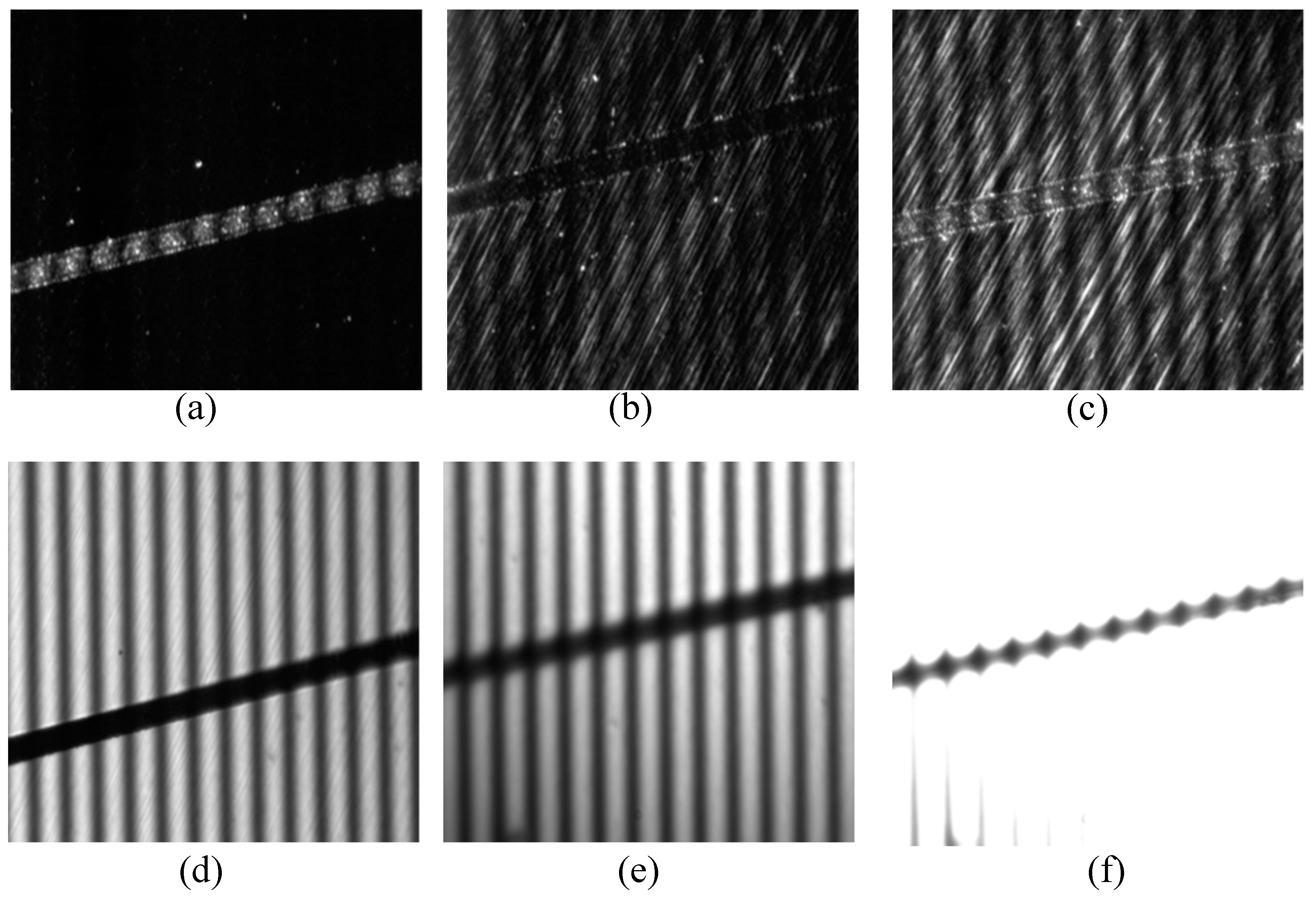
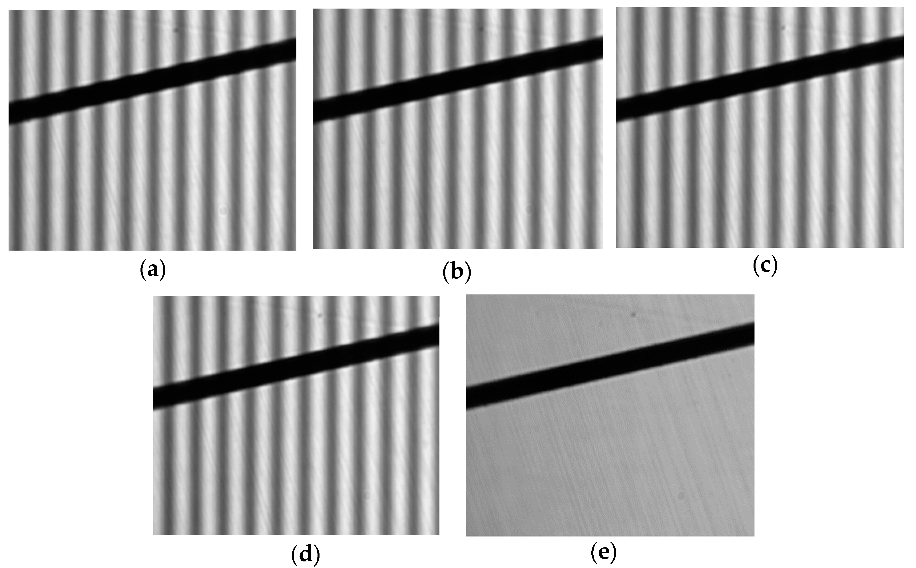
Figure 1a shows the fringe image captured from a semiconductor wafer surface detected using a laser-etched microscale grove with the viewing angle set at zero. As can be seen, the groove area is rather clear but the remaining wafer specular area is almost non-detectable. Therefore, the groove area can be seen with an adequate exposure time because diffuse light is generally weak. With larger viewing angle, the wafer surface becomes clearer with a better image contrast (see
Figure 1b,c). Illustration shown from
Figure 1b–d represents a transition in imaging with increase in viewing angle. When the reflectance relation follows the light reflectance rule, the fringe contrast on the wafer surface reaches its maximum as illustrated in
Figure 1e.
Figure 1f represents the case when the sensor becomes over saturated owing to excessive exposure time.
Figure 1 illustrates the critical reflectance condition of the tested surface under inspection.
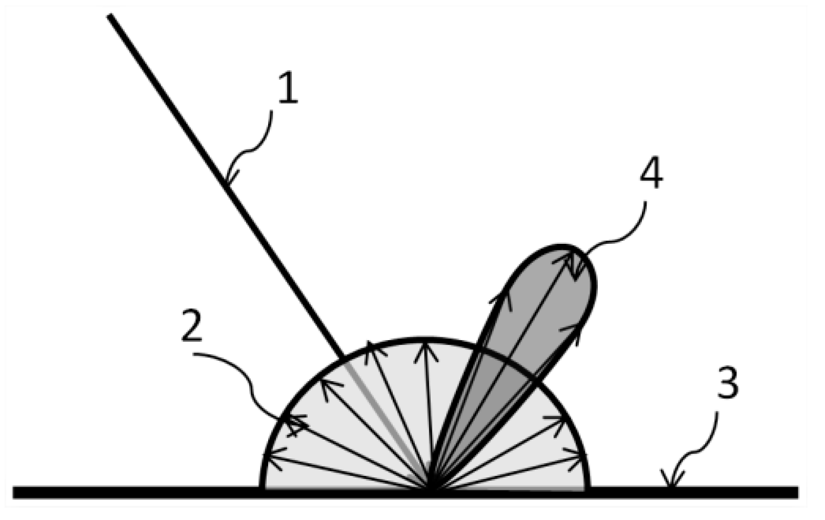
Figure 2 shows the general reflection model of diffuse and specular components when the light is incident from an angle.
To resolve the above issue, this article presents a new optical measuring configuration to capture both of specular and diffuse light reflecting from wafer surfaces. A dual sensing strategy is proposed to detect the light reflection from wafer surfaces when structured fringe projection is used to measure and reconstruct 3-D surfaces. The proposed system design and measuring principle are detailed in the following sessions.
2.1. Optical System Setup
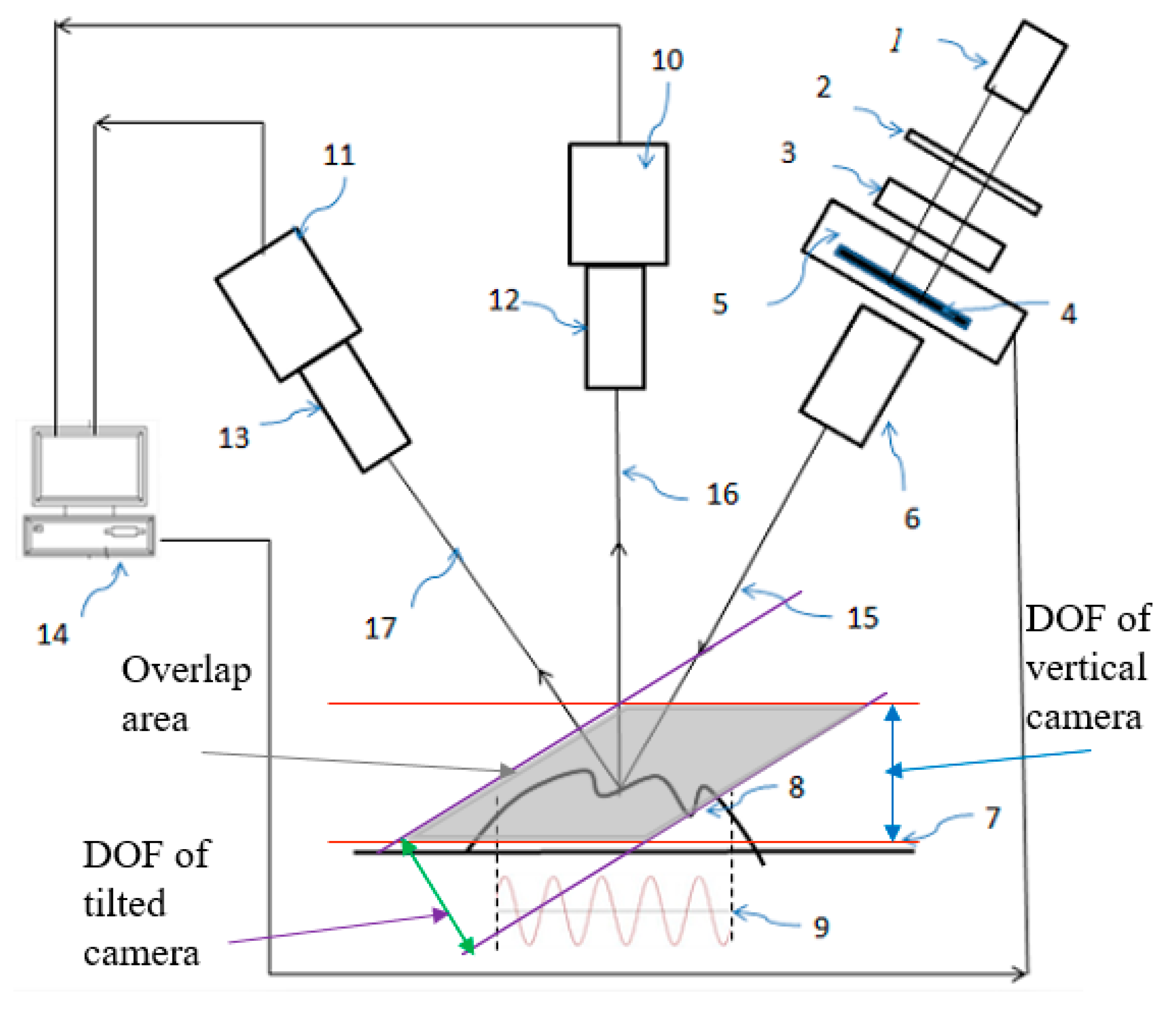
Figure 3 illustrates the optical system configuration of the developed 3-D profilometry. As can be seen, it includes a low-coherent light source (1), a diffuser (2), which is collimated by a lens module (3), a sinusoidal grating (4), and a linear translator (5) for generating an accurate shifted phase. To achieve full-field surface profilometry using PSP, the light source is a low-coherent light source such as LED (light-emitting diode), instead of a coherent one like lasers. In the system, the structured light generated by the incident optical module passes through a telecentric lens (6) and is projected onto the measured surface (8) defined by the reference plane (7). The reflected light passes through two objectives (12 and 13) and is captured by two individual optical sensing cameras (10 and 11). The first objective (12) is arranged in vertical direction to capture the diffuse light while the second objective is set to a reflection angle with respect to the incident projection light angle, so that specular light can be well captured. With such an optical configuration, both diffuse and specular light beams reflected can be well detected by their corresponding objectives. When the projected sinusoidal fringe (9) hits the measured wafer surface, it becomes a deformed fringe according to the phase difference generated by the optical path difference (OPD) between the object profile and the reference plane. The deformed fringe image is transferred to a computer (14) and the phase map is then computed with multi-phase shifting and the wrapping principle using a set of deformed fringe images. Subsequently, phase unwrapping and phase-to-height transformation are performed to extract the profile of the measured surface.
All the optical lenses employed in the developed system are telecentric to ensure the formation of a constant image size along the depth of field (DOF) of the measurement. When the measured surface located inside the overlapped with the DOF of the two cameras (indicated as the gray zone in
Figure 3), the captured image size can be kept constant, so the FOV is kept as a rectangular or square shape according to the image sensor’s design. Meanwhile, to keep the focus plane of the imaging sensor to locate at the same focus plane with the projecting light side, the image sensor can titled with the principle optical axis by an adequate angle to compensate the tilting effect. Thus, both of the focus planes (light projection and imaging) are kept at the same focus plane and the image shape are rectangular or square in the same FOV. Meanwhile, an adequate camera calibration can be performed to identify all the intrinsic and extrinsic parameters of the coordinate transform, so 3D point cloud can be transformed with image coordinates accurately.
2.2. Measuring Principle
2.2.1. Fundamentals in PSP
Using PSP technique for 3-D shape measurement involves several procedures, including projecting sinusoidal fringe patterns onto the object surface, taking the images of the reflected distorted pattern on the object surface, and then calculating the phase map from these captured images. Height information is extracted from the phase map by phase unwrapping and phase-to-height transformation. The calibration coefficients are then employed to transform the 3-D coordinates in image coordinates into world coordinates
of each measured point. The phase
can be computed using light intensities of captured images set by phase-shifted fringe projection. The five-step phase-shifting technique is commonly used because of its accuracy and efficiency. The intensities of the five channels in each pattern can be modeled as follows:
where
is the phase value used by the phase-shifting algorithm in
location,
is the phase-shift,
denotes the intensities of the five captured images for each pixel position,
and
are the intensity modulation and the average intensity for each pixel, respectively.
The phase value of each pixel
can be resolved using Equation (1) as:
where
, are the phase-shift values of each channel.
For the five-step phase-shifting technique () and , the phase value can be computed using the intensity of each channel and the corresponding phase-shift from the five-step phase-shifting technique shown in Equation (2).
With the phase value
being a function of arctangent, the phase value can be obtained in a range from −π to π for phase wrapping. Consequently, if the pixel-based phase difference is larger than 2π, the wrapping phase becomes discontinuous and ambiguous. To obtain a continuous phase map, a phase unwrapping process for subtracting or adding the multiple values of 2π is needed to reconstruct the non-ambiguous phase map. The Gold-Stein phase unwrapping algorithm was employed to extract the unwrapped phase map [
3]. Then, the unwrapped phase difference can be transferred to a height map using the following phase to height transformation.
The phase-to-height transformation is performed using the triangulation technique. The height information of object surface
of each pixel is carried by its phase difference value
, which is measured by the phase difference between the measured phase on the object surface and the reference plane. Since the measured height is generally much smaller than the projection height of the optical system and the projecting objective is telecentric, the object height has a linear relation with the unwrapped phase difference as shown in Equation (3). Thus, the phase value can be transformed by a linear transformation coefficient
K, and the height information of the object is then given as:
2.2.2. Dual-Sensing Technique
As mentioned above, when the projected light beam hits the tested wafer surface, the reflected light beams may contain both diffuse and specular components (see
Figure 2). The diffuse components are mainly formed by reflected light beams from micro structures on wafer surface with high surface roughness. Each reflected beam may interfere with other beams. However, there is no light interference due to low light coherence. In the optical design, the diffuse light intensity is reflected at a wide reflecting angle and can be detected by a vertical sensing camera. On the other hand, specular light is generated by the reflection of incident light from an object with a shiny reflective surface on a flat wafer surface having very low surface roughness. According to the law of reflection, specular light can be detected by an optical objective located at a reflectance angle equal to that of the incident light.
To capture both diffuse and specular components simultaneously, a dual-sensing optical system is developed. In the configuration, a camera (10) is dedicated to capturing diffuse components with another camera (11) designated for capturing specular components. To reconstruct the 3-D shape of the measured surface, the reflected fringe images representing both diffuse and specular beams are simultaneously captured using the proposed system, illustrated in
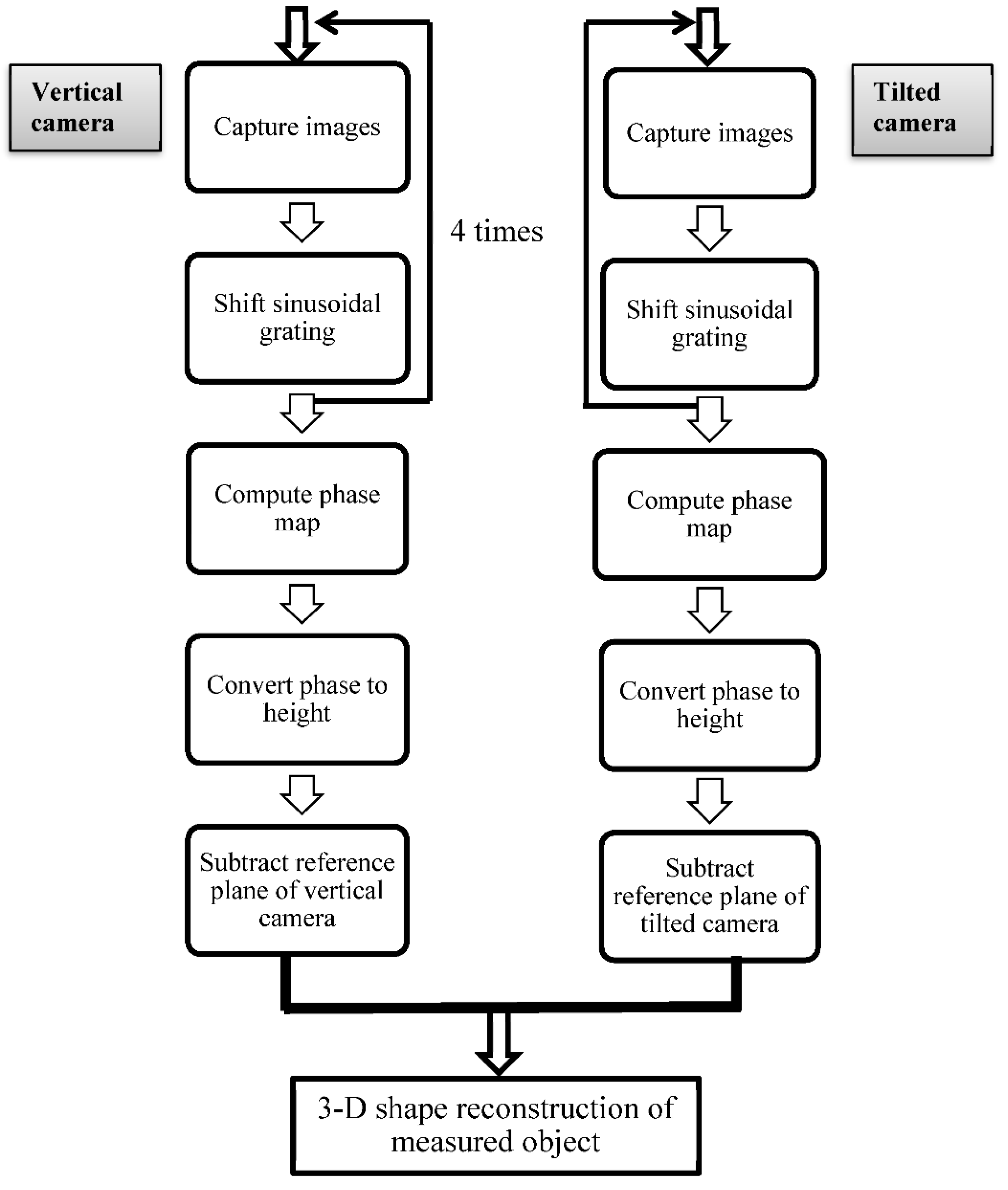
Figure 3. By controlling the adequate duration of light exposure required by the individual cameras, two deformed fringe images with high contrast can be detected. The entire 3-D shape of the measured target surface can be effectively synthesized from the two individual images detected and reconstructed by accurate pixel spatial mapping between two sensors. Details of the proposed measuring system are illustrated by the flowchart shown in
Figure 4.
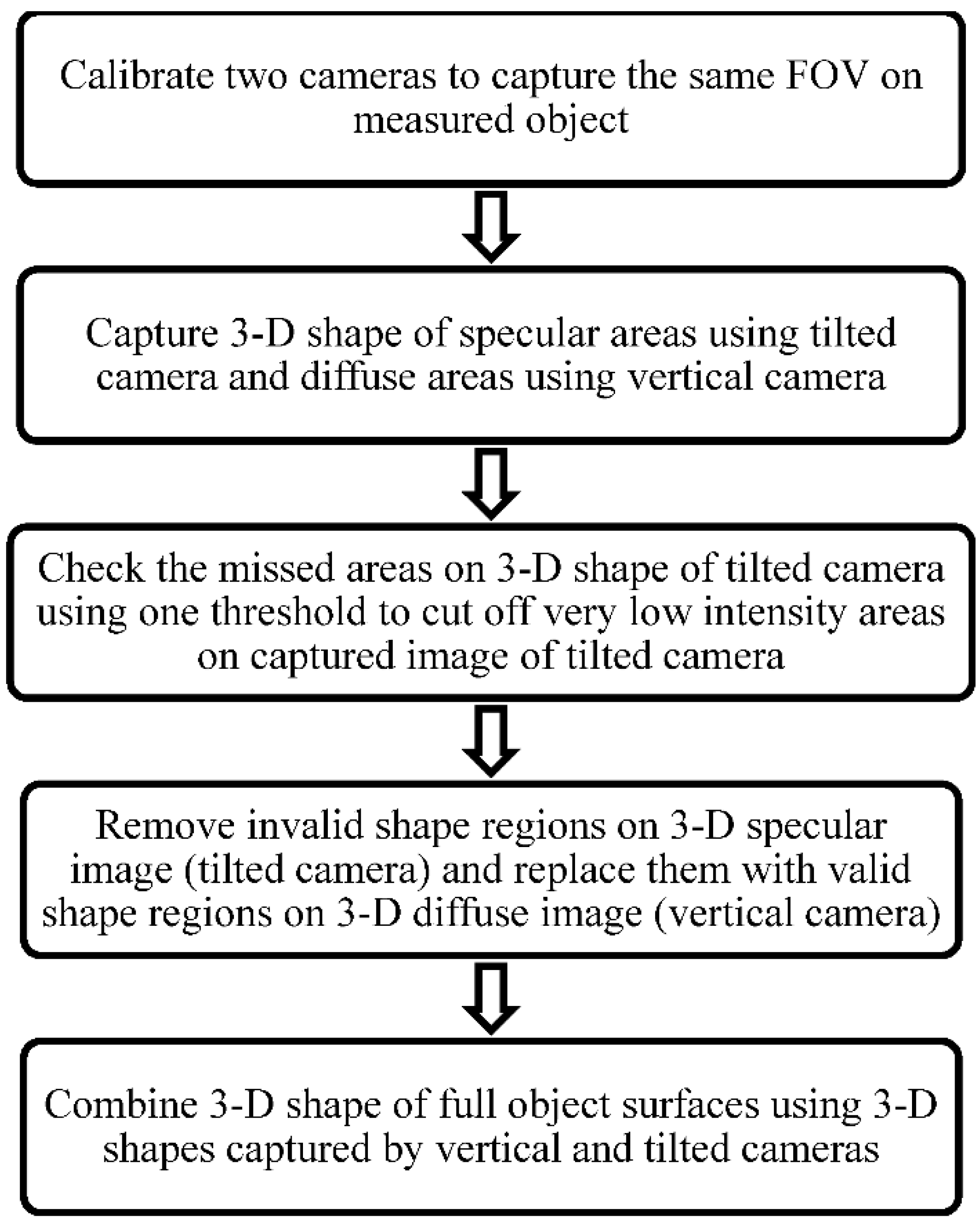
In the proposed technique, the 3-D shape region detected and established from diffuse light can be well synthesized with the 3-D shape region detected and established from specular light. The two surface regions detected can be further merged seamlessly using a camera calibration procedure. A special artifact target is designed and employed as a special mapping target. Two cameras can be calibrated and merged into the same measuring field of view (FOV) on the tested surface. Details of the proposed calibration procedure are illustrated by the flowchart shown in
Figure 5.
2.2.3. Dual Camera Mapping
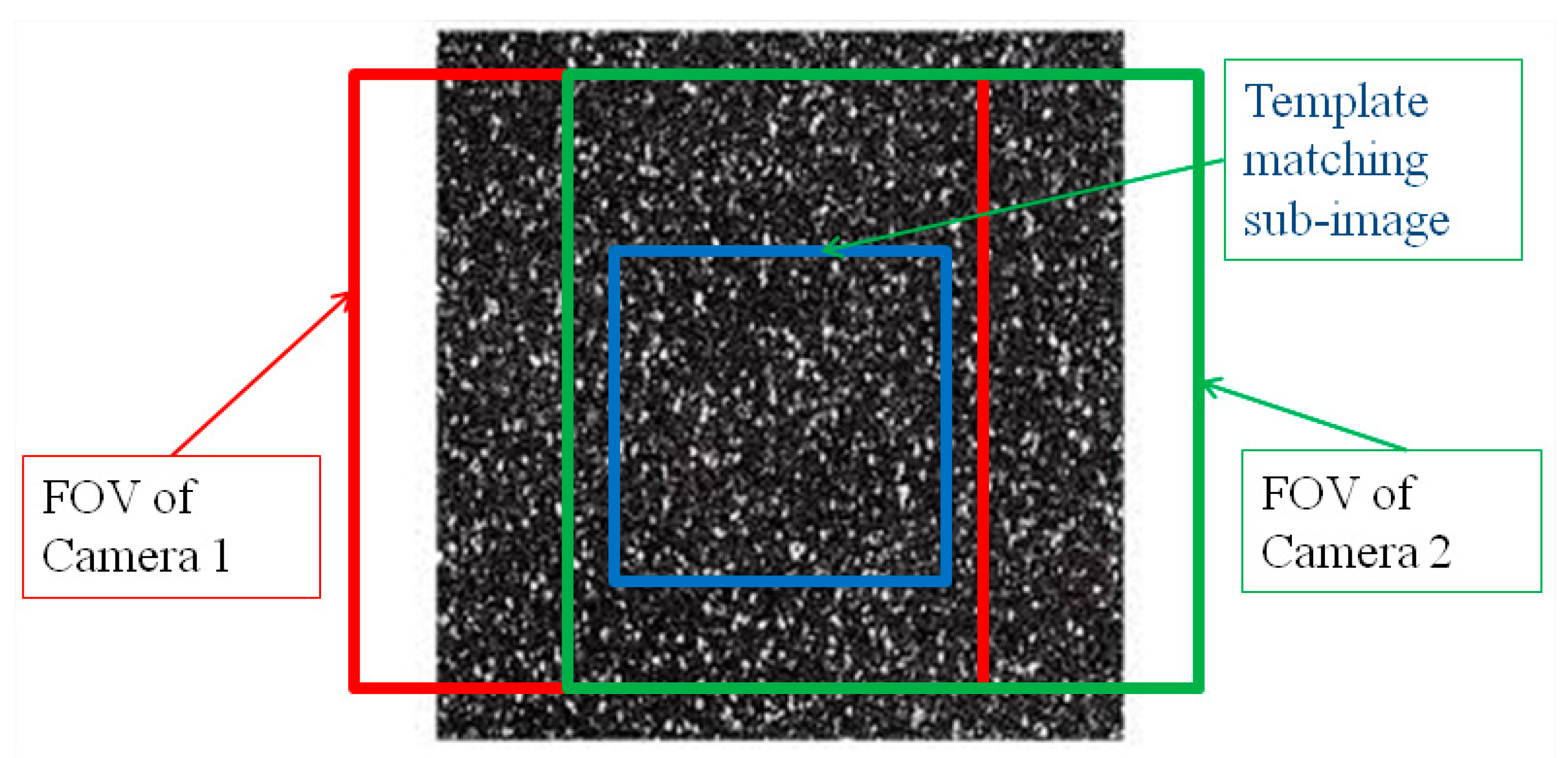
To achieve precise mapping and calibration, an automatic and accurate mapping algorithm was developed to align the two cameras into the same FOV on the measured object.
Figure 6 illustrates the proposed idea of dual camera mapping using random speckles. When mapping images captured by the two cameras, a unique speckle pattern is used and a cross-correlation algorithm is employed to compute the corresponding coefficient. In this study, the following normalized cross-correlation (NCC) algorithm is employed to compute the correlation between images captured by the two cameras.
where:
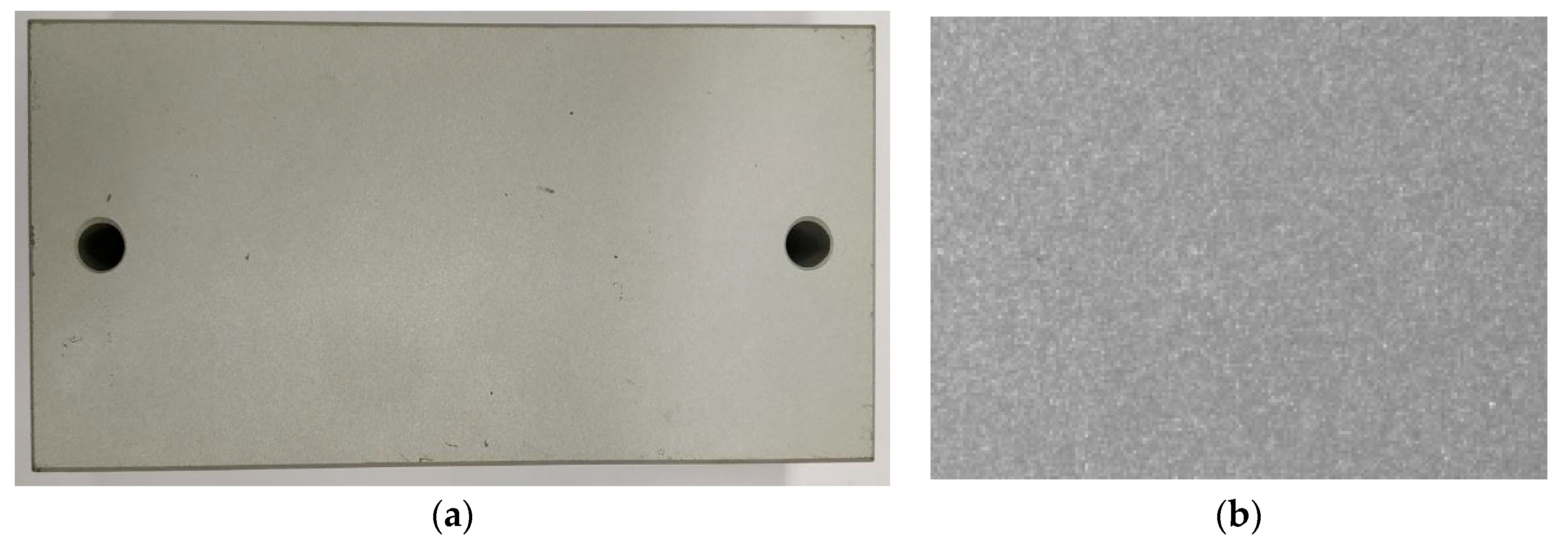
The correlation value ranges from 0.0 to 1.0. The matching score of 1.0 means 100% matching between sub-image and template image. To ensure that the dual camera mapping technique worked well, a correlation threshold is needed to estimate the matching score. It is also important to note that the sub-image size is set to be large enough to retain the accuracy of the matching process. When the sub-image size is too small, the robustness of the correlation technique cannot be assured. In practice, the sub-image size is chosen as a quarter of the captured FOV to achieve good matching and reasonable computation efficiency. To achieve precise image mapping between the two images, a random speckle pattern can be prepared and employed by projecting uniform blue light on an electrostatic-coating aluminum surface with micro random patterns on it. The unique and random speckle pattern can provide accurate image registration for image mapping.
Figure 7 shows the aluminum surface target designed and one of the speckle images prepared for image registration.
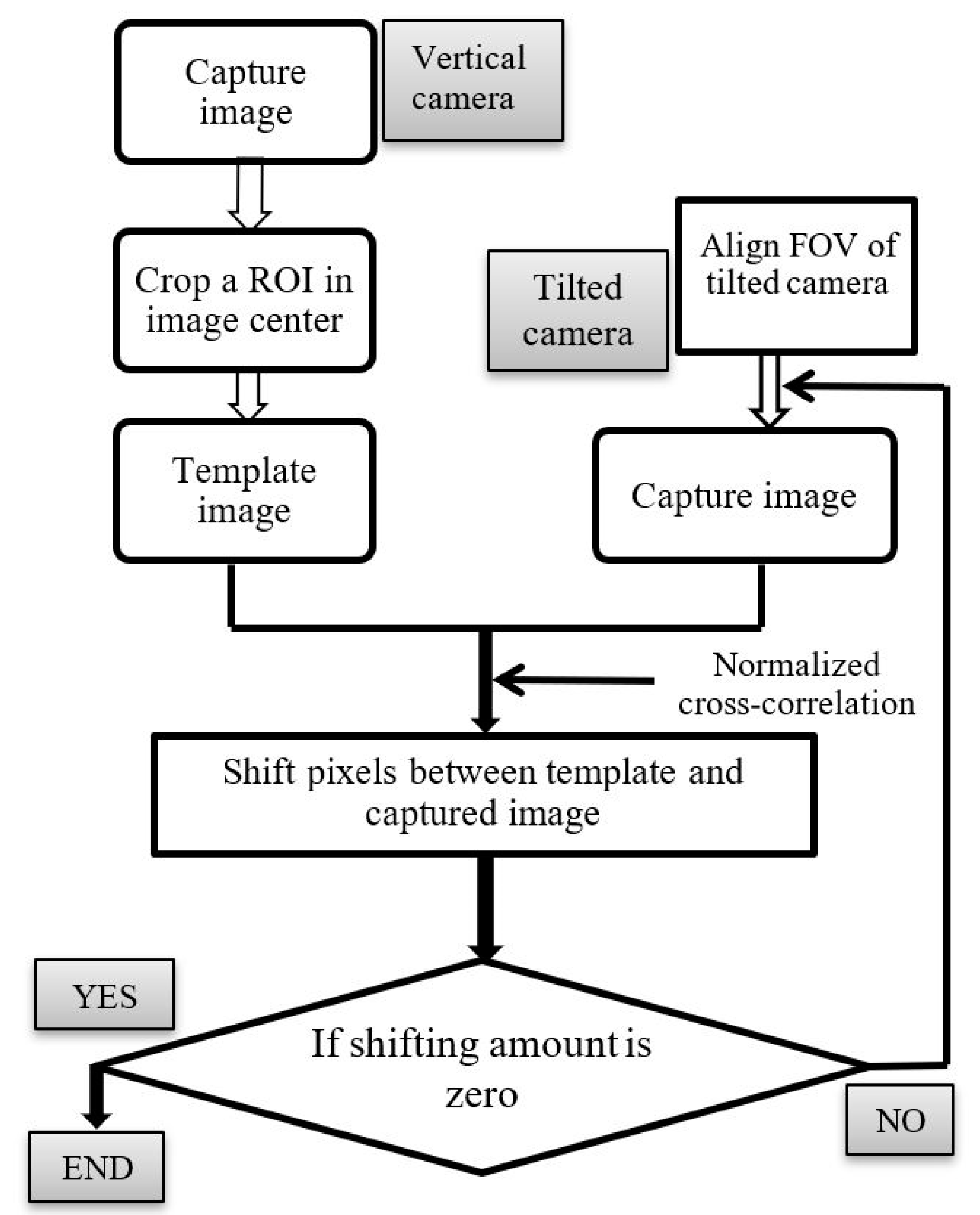
Figure 8 shows the flowchart of the proposed dual camera mapping technique. One sub-image (a quarter of captured image) of the vertical camera is cropped in the image center and selected as a template image. The matching score between the tilted image and template image (vertical camera) is determined using the NCC algorithm. The shifted value between the template image and that captured by the tilted camera can be calculated along the X and Y directions of image coordinates. This parameter can accurately represent the spatial location difference between the FOV of the tilted and the vertical cameras. This process is repeated until the parameter converged to a preset threshold for completion.
2.2.4. Segmentation of Specular and Diffuse Images
An image averaging algorithm is developed to extract specular and diffuse measuring regions with high S/N ratio from the acquired deformed fringe images. Removal of the projected fringe from the acquired fringe is essential for segmentation because these deformed fringes contain light intensity modulation, thus making segmentation difficult. In phase shifting, several phase-shifted sinusoidal patterns are projected onto the tested object and their corresponding deformed fringe images are acquired sequentially. A background image is defined here as an illuminated object image without structured fringes. To obtain the background image of these deformed fringe images, the image averaging algorithm can be performed by simply summing all the phase-shifted images to remove the fringe modulation and generate the background image.
It is important to note that the above algorithm can reliably work even when the reflectivity of the tested surface is extremely variant. The algorithm operates on every individual pixel for the summing; hence, the result is generally insensitive to the pixel intensity. In an experimental test on the algorithm, the sinusoidal projection grating was made by a precise lithography process and a semiconductor’s wafer surface having laser-etched groves was tested. A precise linear stage with positioning repeatability less than 1 µm was adopted to perform four-step phase shifting.
Figure 9a–d illustrates the captured images from the four-step fringe projection with phase-shift 0°, 90°, 180°, and 270°, respectively. As can be seen, all the projected fringes are effectively removed with the image averaging algorithm, and the illustrated object image (also called the background image) is extracted. The experiment result shown in
Figure 9 was acquired by the tilted camera for specular light detection on a smooth wafer surface. An excellent image contrast between specular and diffuse measured regions can be achieved in the background image. The same can be performed on the diffuse images to achieve equal effectiveness.
3. Experimental Design and Result Analyses
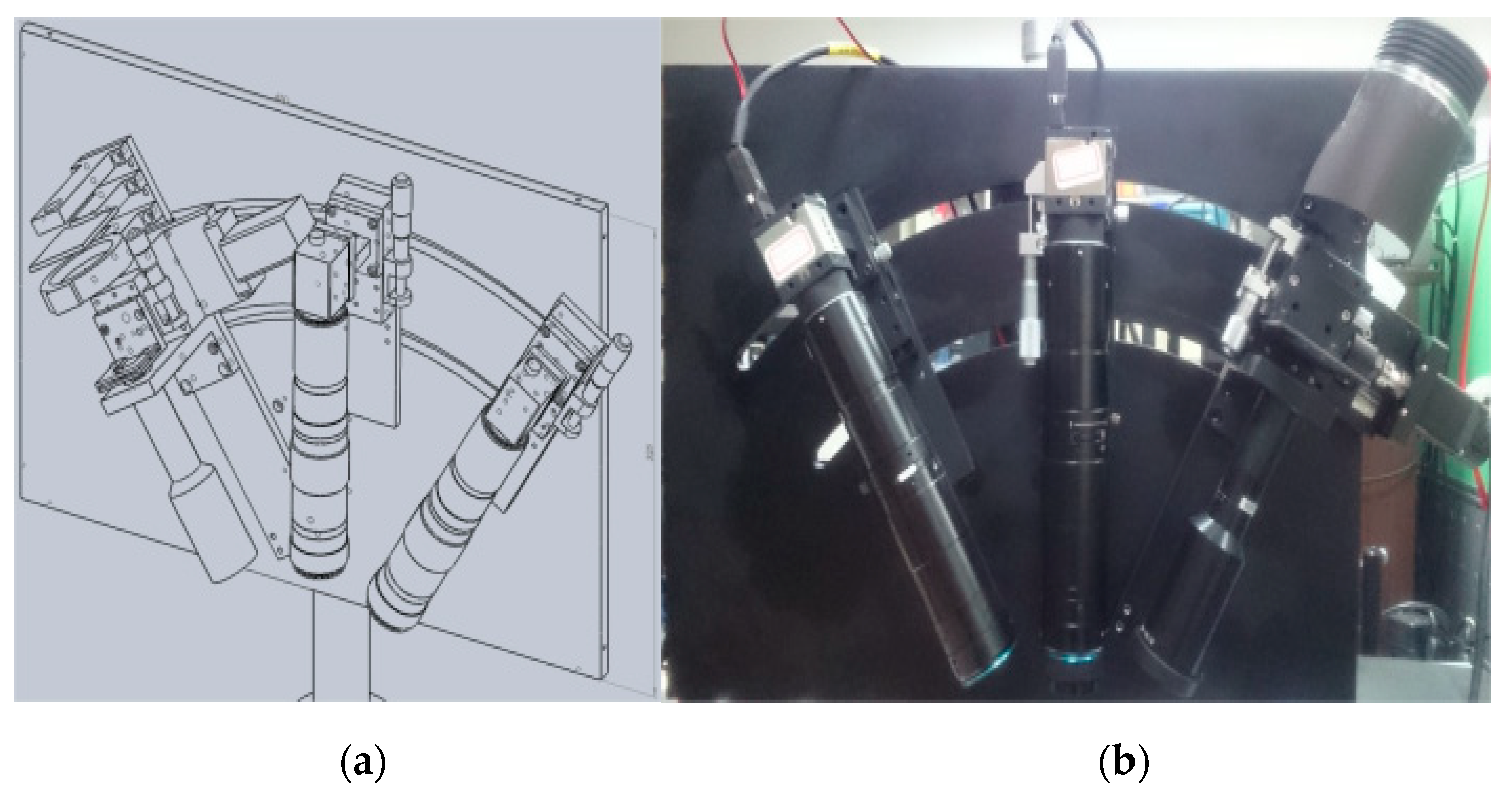
To demonstrate the feasibility and measurement performance of the proposed technique, a 3-D measurement system consisting of two sensing cameras, a single-frequency transmission grating with a period of 24 line pairs per millimeter, and a step motor with positioning accuracy less than 1 µm was developed. Two telecentric lenses with the same optical specification are integrated in front of the two cameras as the optical objective to collimate the reflected diffuse and specular light from the measured object surface. The light module was powered by a 30-Watt white light LED, in which the LED is mounted on a specially designed mechanical radiator for good heat dissipation. A SolidWorks design and hardware of the housing and optical system were implemented and shown in
Figure 10a,b, respectively. The measuring FOV can reach 1.0 × 1.0 mm for every measurement. A maximum measuring depth of the system can reach 1.0 mm which is sufficient for most microstructure profile inspection.
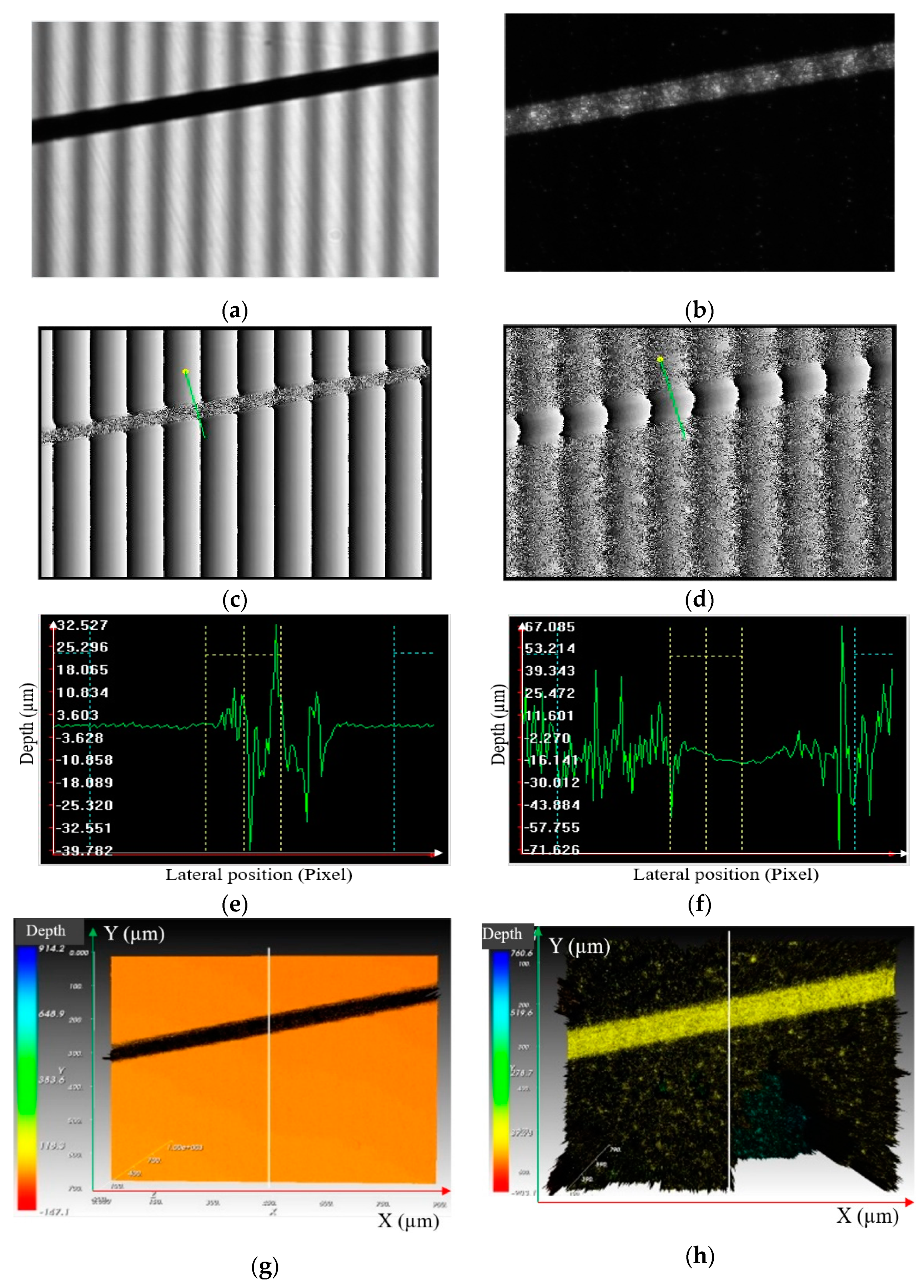
Figure 11a,b shows the fringe images of the tested wafer surface captured using the tilted and vertical cameras, respectively.
Figure 11c,e illustrates the phase map and one height cross-section of the specular wafer surface measured using the tilted camera. Similarly, the phase map and one height cross-section for the laser-etched groove surface regions are measured using the vertical camera simultaneously and shown in
Figure 11d,f. The 3-D profile of groove surface region can be well measured and reconstructed (see
Figure 11h). It is important to note that the 3-D measured shape area of the groove region has random noises due to the non-detectable diffuse light from the laser groove surface region. Nevertheless, this region can be totally recovered and reconstructed by another vertical camera which can capture the diffuse light from the groove region. Two detected 3-D profiles, shown in
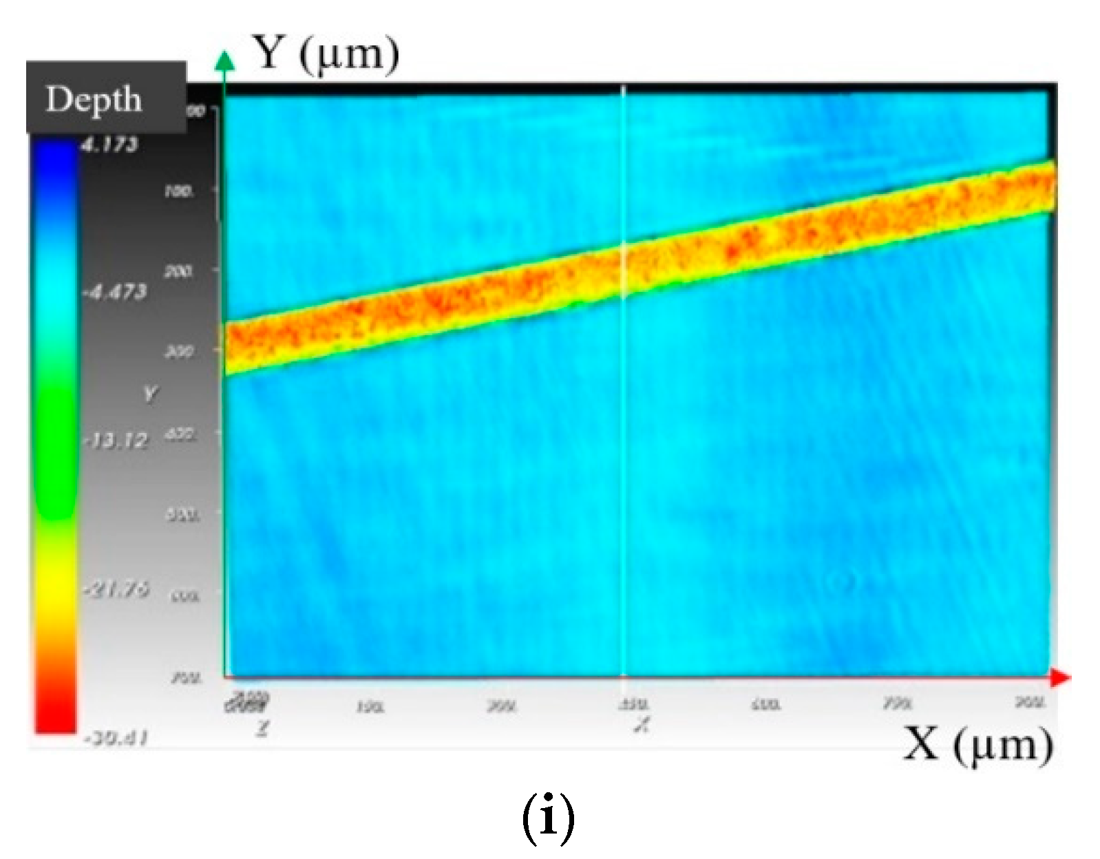
Figure 11g,h, are extracted from their respective original images by the image summing algorithm and further mapped by the camera calibration technique precisely to reconstruct a full-field 3-D profile of the measured wafer, shown in
Figure 11i. These results indicate that the full-field 3-D wafer surface can be measured and reconstructed accurately using the developed technique.
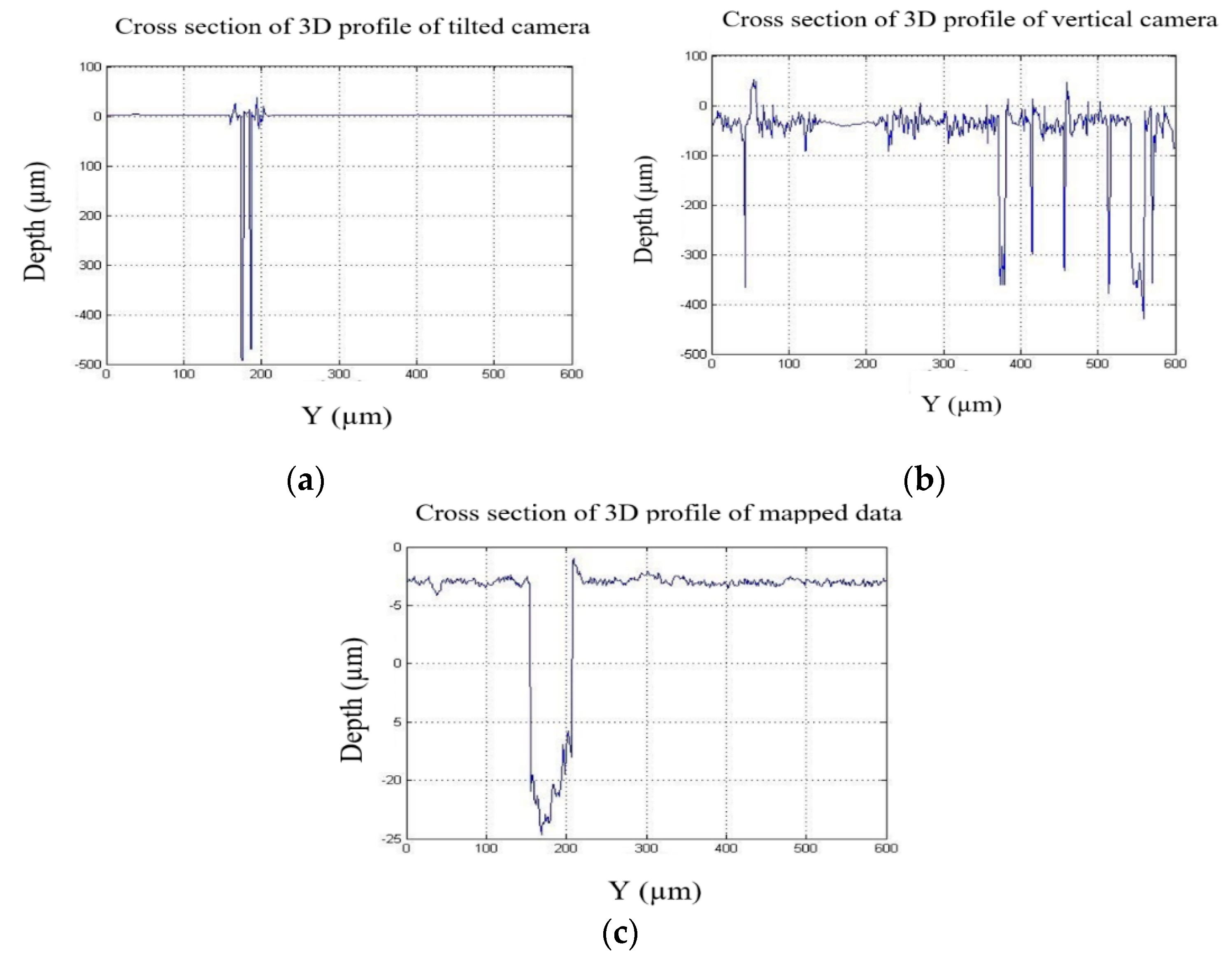
Figure 12 exhibits the measured height cross-section along one lateral section on the tested wafer being captured by the tilted and vertical cameras. The standard deviation of the wafer surface region and groove area are evaluated for measurement precision. In a 30-time repeatability test, the standard deviation in the measured data region, shown in
Figure 12a,b, are 0.265 µm and 1.937 µm, respectively.
The results obtained show that the measurement repeatability can be achieved for less than 2.0 µm when measuring a rough laser-machined wafer surface. With the proposed technique, the measured average step height of the cutting groove on the wafer is 19.01 µm.
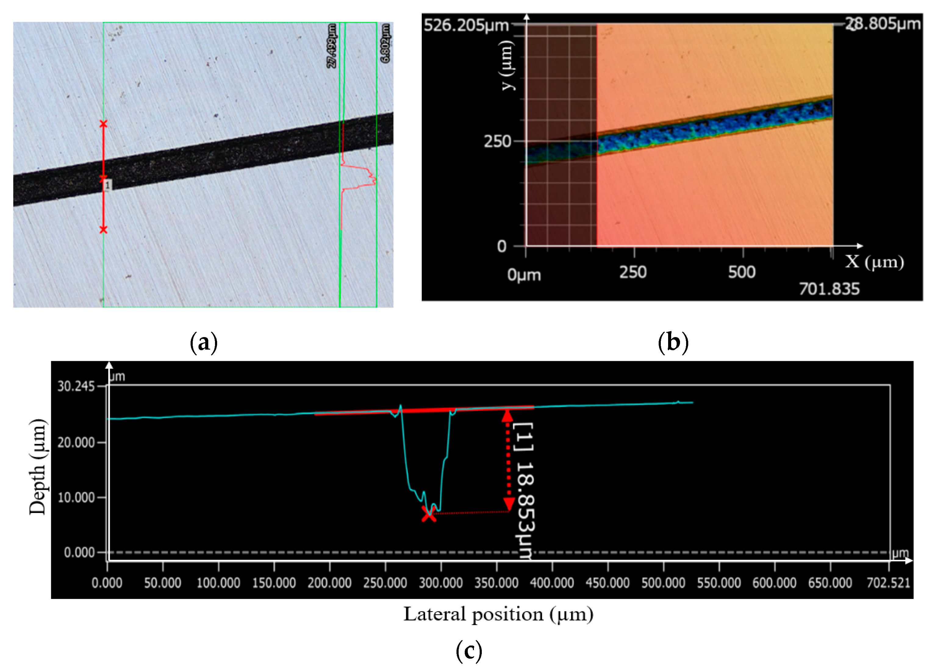
To check the measurement accuracy, the measured result was compared with a pre-calibrated laser confocal microscope.
Figure 13 illustrates the measurement result obtained using a laser confocal microscope (KEYENCE VK-X1000) on the same measured wafer surface region. The measured average step height of the laser-etched groove in a 30-time measurement was 18.853 µm. With the developed method, the measured average step height on the same wafer surface was 20.21 µm, in which the measurement deviation in this case was 1.357 µm.
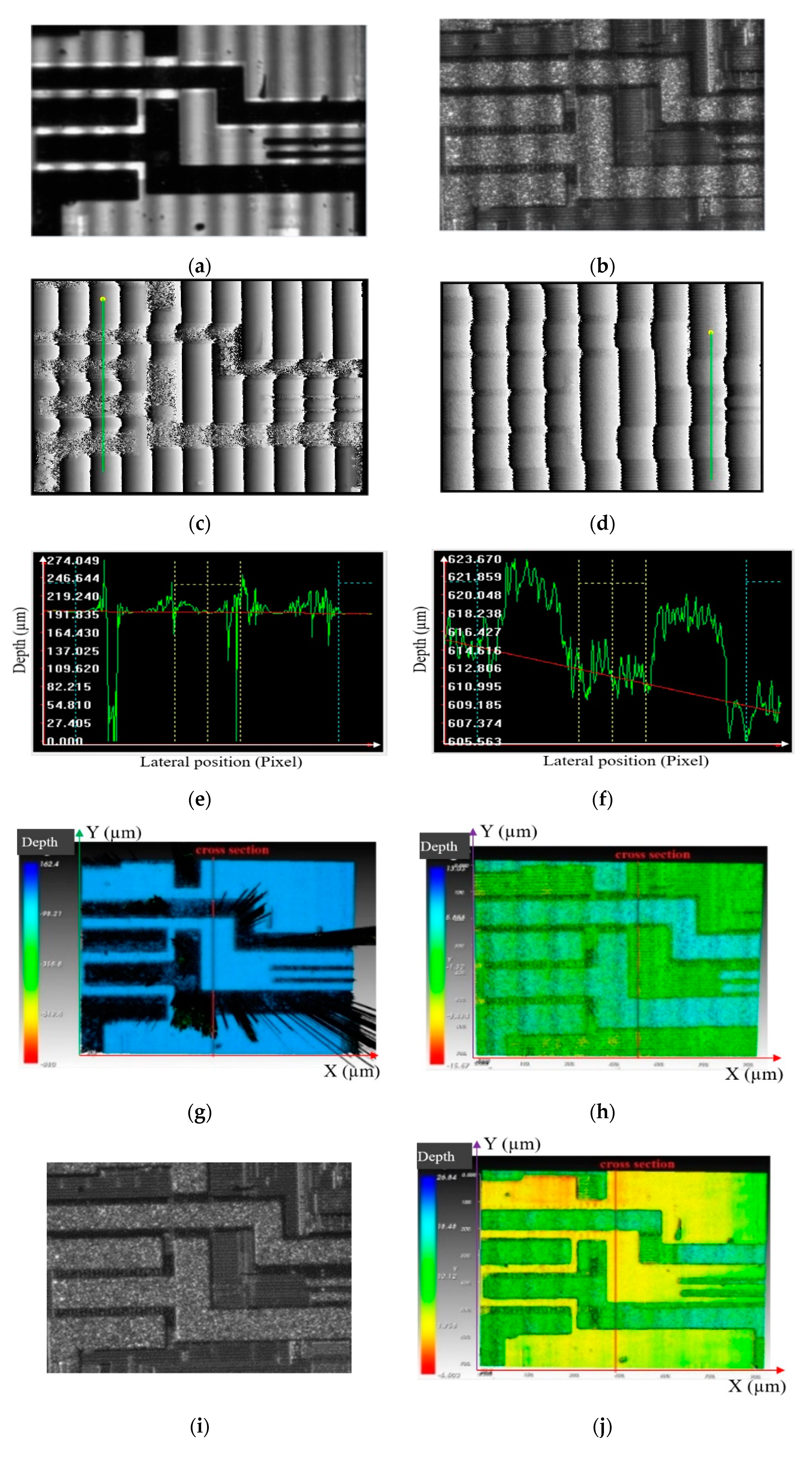
To further check the feasibility of the developed method on an industrial semiconductor parts with variant surface reflectivity, an IC chip was selected for measuring its surface profile.
Figure 14 shows the measured results on an industrial IC surface with extreme reflectivity variance between the substrate and the metal pads. The substrate image detected by specular light is shown in
Figure 14a while the diffuse image detected by diffuse light is illustrated in
Figure 14b. Neither of these two images can cover the entire surface detection. With the developed method, both specular and diffuse images can be detected simultaneously and reconstructed accurately. The phase map and one surface cross-section profile can be reconstructed for smooth substrate surface regions, as seen in
Figure 14c,e, respectively. Similarly,
Figure 14d,f represent respectively the phase map and one surface cross-section profile of the metal-pad regions. Compared with the developed method, the traditional fringe projection method will find excessive noises measured around the IC chip’s pads which are mainly reflected diffuse light areas, as seen in
Figure 14g. By using the developed technique, the surface measurement of the IC chip can be successfully obtained, in which both the pad and substrate areas can be reconstructed simultaneously and accurately, as shown in
Figure 14j. In other words, a significant improvement in surface profilometry of objects with substantial variance of surface reflectance can be achieved with the developed approach.
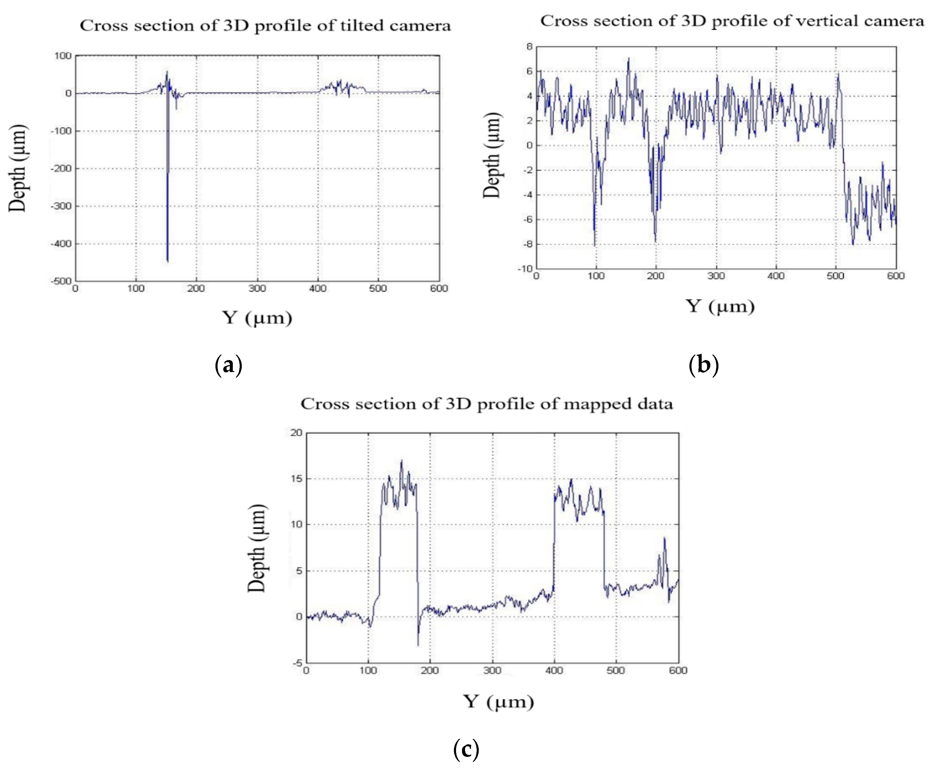
Figure 15a,b illustrate the cross-section of height map at Column 400 on the IC chip imaged by the two cameras in charge of capturing specular and diffuse light, respectively. With the mapping algorithm, the merged cross-section profile can be obtained, as seen in
Figure 15c. The measurement standard deviations of the specular and diffuse surfaces on the IC chip are 0.602 and 1.285 µm, respectively. With the proposed technique, the measured average step height of the metal pads on the IC chip is 13.2 µm.


