Featured Application
High temperature stability multilayers and X-ray optics.
Abstract
A study of the materials properties of WC/SiC multilayer coatings is presented. We investigated the dependence of interface and surface roughness, intrinsic stress, microstructure, chemical composition, and stoichiometry as a function of multilayer period and in some cases compared these to W/SiC multilayer systems. The WC/SiC material pair forms multilayers with extremely smooth and sharp interfaces and both materials remain amorphous over a wide range of thicknesses. These properties are desirable for multilayer-based high-resolution diffractive x-ray optics, such as multilayer Laue lenses (MLLs), which require very thick films in which the layer spacing varies considerably. Thermal and structural stability studies show that WC/SiC multilayers have exceptional thermal stability, making this an extremely robust and favorable material pair for MLLs and other multilayer-based X-ray optical elements.
1. Introduction
Multilayers are “artificial crystals” that can be designed and optimized for specific X-ray optical applications. They are often used when reflectivity, bandwidth, operating angle or some other property has to be optimized beyond the range afforded by natural crystal optics. X-rays interact very weakly with materials, so the scattering efficiency of most structures is very low except under specific circumstances such as those giving rise to constructive interference. This is the case for multilayer films with a period d comparable to the wavelength, λ, of X-rays scattering by an angle 2θ that satisfies Bragg’s condition of λ = 2d sin θ.
Advances in thin film technology including interface engineering, novel materials and material combinations enabled the manufacture of high quality multilayer structures for X-ray applications [1]. In this paper, we explore the properties of the tungsten carbide/silicon carbide (WC/SiC) multilayer system, which has remarkably low interfacial roughness and can form nanometer or even sub-nanometer period multilayers [2,3]. Originally this material pair was investigated as a potential coating for hard X-ray telescopes, which require ultra-thin periods. Here we are particularly interested in other applications such as multilayer-based gratings and multilayer Laue lenses (MLLs) [4].
A MLL [5] is a zone plate or a variable-period transmission grating that diffracts X-rays to a common focus. The resolution of the lens, which is inversely proportional to its numerical aperture (NA), is proportional to the smallest zone width. Hence, multilayers that can form sharp and smooth interfaces at nanometer and sub-nanometer layer thicknesses are of high interest for these novel optics. A MLL is prepared by sputtering a multilayer on a flat substrate, which is then sliced in a direction perpendicular to the layers to create a block of a desired depth, and which is typically several microns thick for hard X-ray lenses. The multilayer periods follow the Fresnel zone plate law [6]:
where n is an integer, λ is the wavelength and f is the focal length and whereby the bi-layer spacing varies inversely with the square root of the layer number. To take advantage of smooth Si wafer substrates (surface roughness of 0.1–0.2 nm) the MLL deposition starts with the thinnest and ends with the thickest period. Unlike a zone plate, a MLL focuses X-rays only in one direction so two MLLs with slightly different focal lengths are needed to produce a focused spot, analogous to two crossed cylindrical lenses. Usually these two MLLs are produced from multilayers made in two separate deposition runs. The depositions can take several days or even longer to prepare multilayers with a total thickness exceeding 100 μm. This requires extreme stability and reproducibility of the sputter deposition process. Of course, due to sputter target consumption, the sputter rate changes over time, which has to be taken into account as well.
rn = (nλf + n2λ2/4)1/2,
Since MLLs consist of layers spanning over a wide range of thicknesses it is of interest to know how the material properties of WC and SiC change as a function of layer thickness. For example, an abrupt amorphous-to-crystalline transition first observed in Mo layers at 2 nm [7] was also noticed in W layers [8]. This transition caused a phase error [9] in a high numerical aperture wedged MLL [10] fabricated from a W/SiC multilayer. It has been shown that presence of carbon delays this transition. For example, in Mo, where this transition occurs at 2.0 nm, it is shifted to 2.6 nm when Mo is in the vicinity of carbon such as in Mo/B4C/Si multilayers [11]. Replacing pure metal with its carbide is another way to prevent nucleation of crystals. In the aforementioned case we replaced W with WC. The new WC/SiC multilayer had no crystalline layers in the whole range of layer thicknesses (3.86 to 21.70 nm) used in these MLLs [8]. A pair of MLLs prepared from these materials was used to demonstrate imaging at 16.3 keV with sub-10 nm focused beam with over 60% diffraction efficiency [8]. In general, high-NA MLLs consist of many thousands of bilayers. For example, the two aforementioned MLLs consist of 5100 and 3326 bilayers. The high NA and high efficiency make such MLLs ideally suited for focusing highly coherent X-ray beams from synchrotrons or X-ray Free Electron Lasers (XFELs). Based on our experience with intense synchrotron beams WC/SiC-based MLLs maintain performance over long periods of time. However, under XFELs beam these lenses would be subjected to more extreme X-ray intensities and potentially damaging conditions. Hence, knowledge of the thermal stability of these MLLs is required to help select materials and design lenses to be used at such sources.
Typically, only materials with low atomic number (Z), low density, high melting point and high thermal stability are considered for XFEL optical coatings and elements. For example, diamond-based Fresnel zone plates were used to successfully focus a hard X-ray FEL beam [12]. However, in XFEL experiments, where the damage of single films [13] and multilayers [14] consisting of high Z elements were studied, higher than expected damage thresholds in grazing incidence geometries were observed. Thus, it may be possible to use MLLs consisting of WC/SiC multilayers with XFEL beams. To the best of our knowledge no thermal stability data were reported for WC/SiC multilayers, and W/SiC systems were only explored at a temperature range below 300 °C [15]. Here we report on WC/SiC and W/SiC multilayers, in particular the study of their properties (interface roughness, microstructure, chemical composition, stoichiometry and stress) as a function of multilayer period. Their stability as a function of temperature and annealing time is investigated as well.
2. Experimental Section
All samples used in this study were prepared in our lab using a magnetron sputtering system with four 7.6 cm diameter magnetrons. W/SiC and WC/SiC multilayers were deposited on super-polished Si wafers using ultra-high purity Kr (99.999%) gas at 0.2 Pa. Depositions were performed at constant powers of 100 W (W target), 100 W (WC target) and 220 W (SiC target). Substrates, which were mounted on a platter, spun at 100 rpm during the deposition. Layer thickness and uniformity was achieved by controlling the platter velocity. Several multilayers of both material pairs (W/SiC and WC/SiC) with different periods ranging from 3.8 nm to 28 nm were prepared and then stored in a dry N2 environment (Table 1).

Table 1.
Stress and surface roughness in as-deposited W/SiC and WC/SiC multilayers of different periods. A dash “-” indicates points where a surface roughness measurement was not performed.
Thermal annealing was performed in a cold wall, high-temperature vacuum (10−7 Pa) furnace with programmed heating and cooling cycles (HSD Engineering Inc., Oakland, CA, USA). Samples were annealed at temperatures from 100 °C to 900 °C. A heating rate of 6.7 °C/min was used to reach the targeted temperature which was controlled within ±2 °C. The listed annealing times refer to the time at the final temperature and do not include the heating and cooling cycle. However, the measurements with different experimental techniques listed below were preformed after each listed annealing temperature cycle, at room temperature. The system was cooled down without any active cooling system until it reached 50 °C at which point the furnace was vented with dry N2.
Small Angle X-Ray Diffraction (SAXRD) and High Angle X-Ray Diffraction (HAXRD) measurements were performed with X’Pert PRO MRD (Panalytical, The Netherlands) equipped with a PIXcel detector, a high-resolution goniometer and a Ge (220) asymmetric four-crystal incidence beam monochromator tuned to Cu Kα radiation (0.15418 nm). SAXRD scans between 0.1°–7° were collected with 0.002° steps. We used the IMD [16] software package to fit the data. HAXRD scans between 30°–80° (90°) were collected to monitor changes in the microstructure of the multilayers.
A Multiple Beam Optical Sensor Ultra-Scan stress system (k-Space Associates, Inc., Dexter, MI, USA) was used to monitor changes in the curvature of the samples before and after each annealing cycle. A two-dimensional (2D) curvature of the sample was mapped with a laser array and subtracted from the sample’s initial curvature. Changes in the beam spacing are related to the stress-induced curvature via Stoney’s equation [17] in which stress is normalized to the multilayer’s total thickness.
Atomic Force Microscopy (AFM) images were obtained on bare Si substrates, and multilayer-coated W/SiC and WC/SiC samples (before and after annealing) with a Dimension Icon (Bruker, Karlsruhe, Germany) microscope. This AFM is equipped with an acoustic hood and vibration isolation table with noise floor of less than 0.03 nm RMS. The probe tips (Si doped with Sb) had a tip radius of 8 nm and a resonance frequency of 75 kHz. Atomic force micrographs across 1 μm × 1 μm areas (512 × 512 pixels) were collected in a tapping mode at a 1 Hz scan rate and processed using the Bruker NanoScope Analysis software. These measurements give multilayers’ surface high spatial frequency roughness, which is referred as “Roughness” in the tables below.
Rutherford Backscattering (RBS) analysis (Evans Analytical Group, San Diego, CA, USA) was used to obtain quantitative depth profiles of Si, C and W, and the stoichiometry of SiC and WC layers. Due to the limited depth resolution of the RBS method, samples had to consist of much thicker SiC and WC layers than used in multilayers listed in Table 1. Consequently, samples for RBS analysis consisted of only one pair of SiC and WC layers, each 40 nm thick. After deposition the sample was cut in half. One half was annealed at 700 °C for 24 h while the other was kept as a control. Both samples were exposed to 2.275 MeV He++ ion beam at normal incidence angle and RBS spectra were collected with a normal angle detector at 160° and a grazing (movable) detector at ~100°.
Samples for Transmission Electron Microscopy (TEM) were prepared using in situ FIB lift-out technique on an FEI Dual Beam FIB/SEM (Evans Analytical Group, San Diego, CA, USA). TEM images were obtained with an FEI Tecnai TF-20 FEG/TEM operated at 200 kV in bright-field (BF), dark-field (DF) and high-resolution (HR) TEM mode.
3. Results and Discussion
Typically, multilayer periods in a MLL range from few nanometers to several tens or even hundreds of nanometers. It is thus important to explore how their properties change as a function of layer thickness as well as a function of temperature. Here we investigate periodic multilayers of different period thickness, which can be considered sections of an MLL.
Table 1 lists the initial (as-deposited) stress and surface roughness (as described in Experimental Section) of W/SiC and WC/SiC multilayers of various periods. Within the measurement error the initial surface roughness is the same as the surface roughness of the bare Si wafer. Slightly higher surface roughness was measured only on multilayers with periods above 14 nm.
Figure 1 shows normalized periods of nine W/SiC multilayers with initial thicknesses between 2.15 nm and 26.66 nm and two WC/SiC multilayers with initial thickness of 3.81 nm and 28.63 nm, whose initial period, stress and surface roughness are also listed in Table 1. It exhibits the effect of the temperature on the multilayer period for multilayers of different period thicknesses. The multilayer period changed (contracted) by less than 0.5% relative to the multilayer period in most cases. Multilayers annealed above ~400 °C show larger contraction (W/SiC) or expansion (short period WC/SiC) with the exception of large period WC/SiC multilayer. If not mentioned otherwise the annealing time was 1 h. Only one multilayer delaminated, indicated by a blue star in Figure 1. This happened to the W/SiC multilayer with an initial period of 3.8 nm when annealed to 850 °C. All other multilayers in this study, including the WC/SiC multilayer annealed to 900 °C, showed no cracking or delamination.
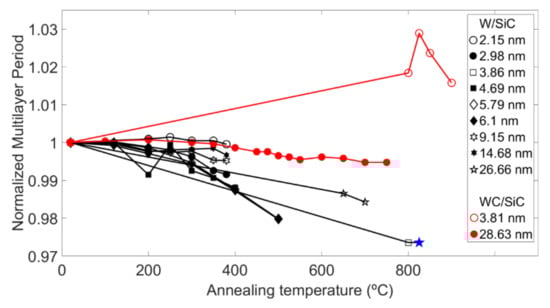
Figure 1.
Normalized multilayer period of W/SiC (black) and WC/SiC (red) multilayers as a function of annealing temperature. The blue star indicates the point where the W/SiC multilayer delaminated from the silicon substrate.
Stress evolution in W/SiC multilayers as a function of period thickness (Table 1) is interesting as well. An increase in stress towards more negative (more compressive) stress is observed between 6 nm and 9 nm multilayer period. This region coincides with the region where the microstructure of W layers changes from amorphous to polycrystalline [8]. After this transition stress relaxes (gets less compressive) but with increasing period grows again towards more negative (more compressive) stress (Figure 2 and Table 1).
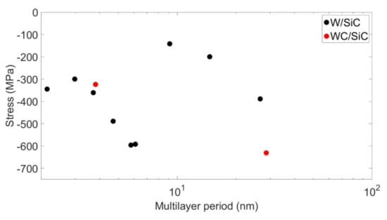
Figure 2.
Stress in as-deposited W/SiC (black) and WC/SiC (red) multilayers as a function of multilayer period.
Table 2 lists period, stress and AFM surface roughness associated with a long period WC/SiC (28.6 nm) multilayer as a function of annealing temperature. It demonstrates that both period and surface roughness remain unchanged up to 700 °C.
Table 2.
WC/SiC multilayer period, stress and surface roughness as a function of annealing temperature. These data were collected on the same 100 bilayer multilayer (28.63 nm), which was measured after each annealing step. Roughness is AFM measured surface roughness.
Short period (3.8 nm) WC/SiC has not been measured as extensively (Table 3). However, it was annealed and investigated at higher temperatures and also for different lengths of time. We will first comment on the period and the surface roughness change. Annealing the sample to 700 °C resulted in a negligible change in period thickness (Table 3). SAXRD plots are remarkably similar when one compares samples annealed at 700 °C for 1 h, 6 h or 24 h (Figure 3). Surface roughness, as measured with AFM, shows a small increase from 0.16 nm in as-deposited sample to 0.20 nm in a sample annealed to 700 °C for 24 h (Table 3). However, this is hardly seen in SAXRD spectra (Figure 3). At 800 °C we still do not see any noticeable change in SAXRD spectra (Figure 4) except a slight increase in the period thickness (Table 3). The sample annealed at 825 °C starts showing signs of modifications. Most noticeable is the region between the 1st and 2nd Bragg peaks. However, longer annealing time at this temperature (9 and 17 h) show visible decrease in Bragg peak intensities and an increase in surface and interface roughness (Figure 5). Going just slightly higher in temperature to 850 °C, similar change in SAXRD spectrum can be observed only after 1 h anneal (Figure 4). The sudden drop in Bragg peak intensities is correlated with period thickness and surface roughness increase (Table 3). However, it took 9 h at 825 °C before the surface roughness changed from 0.24 nm to 1.40 nm. It is obvious that we have to consider the whole spectrum of measurements, and not only period thicknesses, to evaluate thermal stability.
Table 3.
WC/SiC multilayer period, stress and surface roughness as a function of annealing temperature. Data after “as-deposited” originate from the same sample. Data from six different, short period samples are shown here. Roughness is AFM measured surface roughness.
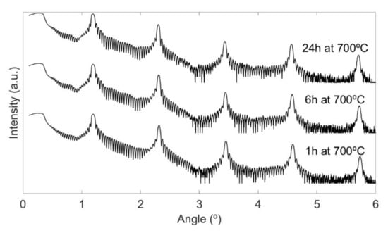
Figure 3.
SAXRD spectra of a short (~3.8 nm) period WC/SiC after being annealed at 700 °C for 1 h, 6 h, and 24 h. This multilayer consists of 30 bilayers.
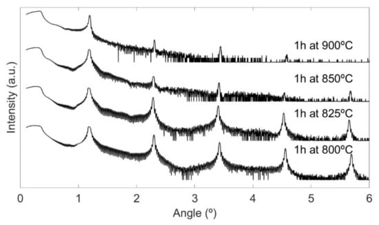
Figure 4.
SAXRD spectra of a short (~3.8 nm) period WC/SiC after being annealed to 800 °C, 825 °C, 850 °C and 900 °C. This multilayer consists of 50 bilayers.
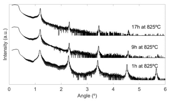
Figure 5.
SAXRD spectra of a short (~3.8 nm) period WC/SiC after being annealed at 825 °C for 1 h, 9 h and 17 h. This multilayer consists of 50 bilayers.
The multilayer intrinsic stress also changes with temperature. Independent of their period thickness all multilayers studied here initially had a compressive stress (Table 1). We define negative stress as compressive and positive stress as tensile. The initial stress of a long period WC/SiC multilayer is −631 MPa while the stress measured in the short period multilayer is −310 MPa. The former was annealed sequentially in steps of 100 °C, 50 °C or 25 °C between 100 °C to 700 °C (Table 2). The stress crossed the zero point at around 350 °C and became tensile with further increase in temperature. At 700 °C (last point in Table 2) the stress was tensile, at 657 MPa (absolute stress). This is a difference of ~1300 MPa as compared to the initial stress. The initial stress in short period multilayer was −300 MPa. Up to about 300 °C stress development for short and long period multilayers are similar. However, at temperatures >300 °C short period multilayer shows smaller changes as compared to the long period multilayer. At ~800 °C there is an inflection point where stress starts decreasing (Figure 6). The inflection point correlates well with the temperature where Bragg peak intensities drop and an increase in interface and surface roughness is observed.
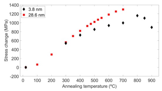
Figure 6.
Stress change as a function of annealing temperature for two WC/SiC multilayers of different multilayer periods. All data displayed here are for annealing times of 1 h.
To better understand observed changes we show fits of the diffraction spectra from W/SiC and WC/SiC multilayers in as-deposited states and after annealing them to 700 °C for 24 h. Figure 7 displays experimental and fitted data of a 25-bilayer W/SiC multilayer with a period of 3.96 nm. Based on this fitting, Γ, defined as the ratio between the thickness of the W layer and the multilayer period is 0.4 (Γ = dW/(dW + dSiC)). A slight shift in Bragg peaks towards larger angles in the annealed sample indicates period contraction from 3.96 nm to 3.75 nm. We also observed an increase in the peak intensity of the 5th Bragg peak, which indicates a change in the ratio between the absorber and the spacer layer thickness. The fit result indicates a decrease in Γ from 0.4 to 0.3 after anneal. The change in the intensity of other peaks, especially 2nd and 3rd Bragg peaks, is also noticeable. This indicates slightly smoother or wider interfaces in the annealed sample (0.28 nm vs. 0.22 nm). Our model assumes period consisting of only two layers, SiC and W, and does not include any interface or inter-diffusion layers. Obviously a more sophisticated model is required to fully describe the measured spectra.
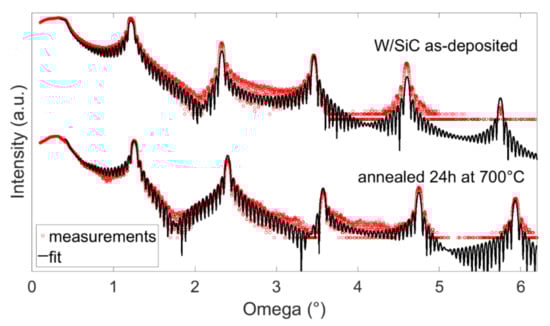
Figure 7.
SAXRD experimental data and fits of the same W/SiC multilayer before and after anneal at 700 °C for 24 h.
W/SiC multilayers with similar periods were previously investigated for thermal stability [15] however, only up to 300 °C. In that paper it is reported that W/SiC revealed no significant changes when annealed to 100 °C. A slight increase in the reflectivity of the 1st Bragg peak was reported for multilayers heated to 300 °C for 1 h.
In our study, we observed an increase in the 1st Bragg peak intensity already when sample was annealed to 120 °C for 1 h. The intensity of the first Bragg peak continued to increase with temperature (data points were collected at 200 °C and 300 °C). However, at 400 °C the intensity dropped and was comparable to that in the initial, as-deposited state. At temperatures of 500 °C and above the intensity of the 1st Bragg peak intensity decreased with increasing temperature.
Figure 8 shows experimental data and fits of diffraction spectra from a 30-bilayer WC/SiC multilayer before and after it was annealed to 700 °C for 24 h. As already indicated in Figure 3 this multilayer remained very stable at this temperature even for extended annealing time. The measured period expansion was small, from 3.85 nm to 3.88 nm. The initial value of Γ of 0.56 changed to 0.63, opposite to what we observed in the W/SiC multilayer (Figure 7).
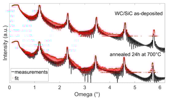
Figure 8.
SAXRD experimental data and fits of the same WC/SiC multilayer before and after anneal at 700 °C for 24 h.
Based on these results the observed changes seem to be diffusion driven. WC/SiC annealed to 700 °C shows a slight increase in period and surface roughness as a function of annealing time. Stress, which is initially compressive (−234 MPa) becomes tensile (676 MPa) and does not change with prolonged time at this temperature. Spectra measured in a sample annealed to 700 °C for 24 h look almost identical to the spectra obtain from a sample annealed to 825 °C for 1 h (Figure 3 and Figure 4). Keeping the multilayer at 825 °C much longer causes a noticeable increase in the interface and surface roughness and a stress decrease. This is different to what we observed in W/SiC multilayers where the period consistently decreased with increasing temperature. Also, when annealed to 850 °C for only 1 h W/SiC multilayer delaminated from the substrate (Table 4).
Table 4.
W/SiC short multilayer period, stress and surface roughness as a function of annealing temperature. Data following as-deposited sample originate from the same sample.
Further information on the microstructure can be obtained from HAXRD spectra. First we plot different period multilayers in as-deposited state (Figure 9 and Figure 10). They all exhibit two sharp peaks at 33.1° and 69.2° identified as Si (100) coming from the Si single crystal substrates. W/SiC multilayer with 2 nm period consists of amorphous layers and shows no peaks between Θ = 30° and 90° (Figure 9). With the period increase to 5.8 nm a broad peak centered at around Θ = 38° becomes noticeable. With further increase in the period thickness to 9.1 nm this peak becomes narrower, shifts to ~40° and can be identified as W(110) [18]. This particular multilayer shows two additional peaks, one centered at Θ = 73° and the other at 87°, corresponding to W (211) and W (220) [18], respectively. All aforementioned peaks become more intense and narrower with further increase in the period thickness (e.g., 21 nm period multilayer).
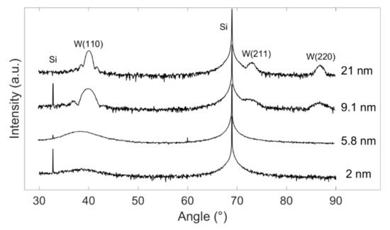
Figure 9.
HAXRD scans of as-deposited W/SiC multilayers of different multilayer period thicknesses.
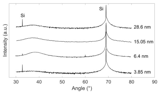
Figure 10.
HAXRD scans of as-deposited WC/SiC multilayers of different multilayer period thicknesses.
The analogous HAXRD spectra of WC/SiC samples in as-deposited state are featureless (Figure 10) apart from two already mentioned peaks associated with the Si substrate. This implies that both SiC and WC are amorphous in multilayers with periods between 3.85 nm and 28.5 nm with nominal Γ = 0.5.
Heating to 700 °C for 1 h increases peak intensities of W (110) and W (211) in 21 nm period W/SiC multilayer as seen in Figure 11 indicating an increase in crystal size of W crystals with increasing temperature. However, annealing WC/SiC multilayer of a similar period (28.5 nm) under the same conditions causes almost no change (Figure 11).
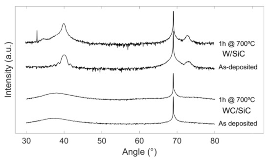
Figure 11.
HAXRD spectra of as-deposited and annealed W/SiC (21.3 nm) and WC/SiC (28.5 nm) multilayers. The samples were annealed to 700 °C for 1 h.
In short period multilayers (3.8 nm), hence below W amorphous-to crystalline transition, both W/SiC and WC/SiC show no crystalline phase either before or after anneal to 700 °C (Figure 12). In this case, all layers remained amorphous even after being annealed for 24 h at this temperature.
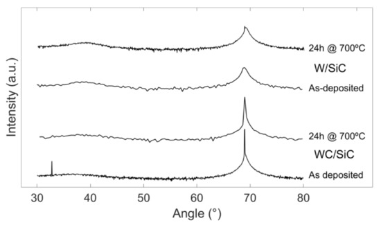
Figure 12.
HAXRD spectra of as-deposited and annealed W/SiC (3.8 nm) and WC/SiC (3.8 nm) multilayers. The samples were annealed to 700 °C for 24 h.
Cross-section TEM images of WC/SiC multilayer also show no changes in the microstructure of this multilayer annealed to 700 °C for 24 h (Figure 13). In particular, there is no indication of crystals in any of the two materials, consistent with the results obtained with different methods presented above. The electron diffraction pattern (insert) shows Bragg spots but these are due to the single crystal Si substrate. This is because the used beam was large and illuminated both the multilayer and the substrate, simultaneously. The slightly stronger diffuse ring observed in the annealed sample (Figure 13a) can be explained with a longer exposure time. Based on electron diffraction, high resolution TEM and dark field imaging (not shown here) we conclude that the layers are amorphous not only in as deposited multilayer but also after annealing to 700 °C for 24 h.
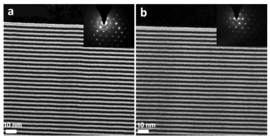
Figure 13.
Cross section TEM images of the same WC/SiC multilayer as deposited (a) and after annealing to 700 °C for 24 h (b); Annealing increased the multilayer period from 3.84 nm to 3.88 nm. The electron diffraction pattern in the upper right corner shows Bragg spots from the substrate (single crystal Si) and faint diffuse ring due to the multilayer. Difference in the intensity of this ring is due to different exposure times.
Since both materials in WC/SiC multilayers are alloys we are also interested in the elemental composition of the sputtered layers and any changes induced by high temperature annealing. RBS spectra of two identical samples, as-deposited and annealed to 700 °C for 24 h were measured (for details see Experimental Section). They show identical composition to within experimental error. The analysis was repeated several times to confirm these results. Figure 14 shows a full RBS spectrum of as-deposited WC/SiC sample and a zoomed region corresponding to W in WC layer.
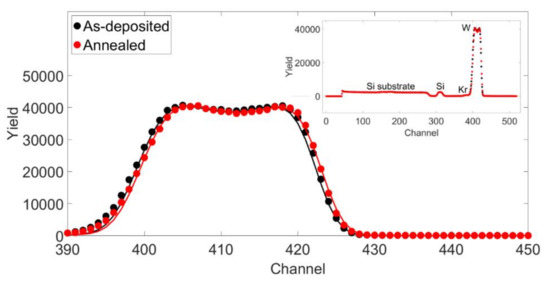
Figure 14.
The plot in the top right corner shows full RBS spectrum of as-deposited and annealed WC/SiC sample, consisting of only two layers, each 40 nm thick and deposited directly on Si substrate. These two spectra are basically indistinguishable. Peak between channel 50 and 280 comes from the Si substrate. The small peak at ~310 is due to the Si in the SiC layer. The peak between 370 and 400 is due to Kr and between 390 and 420 is the W in the WC layer. Experimental data of W peak in as-deposited sample (black dots) with theoretical fit (black line) and of annealed sample (red dots) with theoretical fit (red line) are plotted again in the main plot to show details.
The densities of WC and SiC (atoms/cm2) were calculated empirically from the bulk elemental densities, and used to calculate the RBS thicknesses (Table 5 and Table 6). Using equation:
one can calculate the density (atoms/cm3) if the thickness is known. In this equation TRBS is RBS thickness obtained via fitting the data and DRBS is the assumed density. In as-deposited sample 40 nm thick SiC appears to be homogeneous with a Si:C ratio of 47.6:52.4. However, WC shows an elemental composition gradient. Hence, the 40 nm layer was subdivided into three 13 nm thick layers and fitted with different elemental composition ratios. In addition to W and C this layer also showed measurable amount of Kr (1.4 at%) sputtering gas. The sequence of bulk/WC/SiC layers can be described as bulk/(13 nm + 13 nm + 13 nm) WC/(40 nm) SiC. The W:C elemental composition is (46.0:52.6) + (37.2:61.4) + (43.8:54.8) as listed in Table 5. Tungsten is noticeably depleted in the middle of WC layer (Figure 14). Annealed sample has an identical elemental composition in the layers and sub-layers to within experimental error. The only difference is in the sub-layer thicknesses. The best fit could be obtained with bulk/(14 nm + 13 nm + 12 nm) WC/(40 nm) SiC (Table 6).
Dreal = (DRBS x TRBS)/Treal,
Table 5.
Thickness, atomic concentrations and assumed densities of SiC (layer 1) and WC (layers 2–4) and Si substrate (bulk) in as-deposited state as determined from RBS analysis and fits.
Table 6.
Thickness, atomic concentrations and assumed densities of SiC (layer 1) and WC (layers 2–4) and Si substrate (bulk) after annealing at 700 °C for 24 h as determined from RBS analysis and fits.
4. Summary and Conclusions
Layers of W and Si create structures of very high contrast in electron density, making them attractive for applications at photon energies above 10 keV. Previous studies showed that replacing tungsten with tungsten carbide and silicon with silicon carbide further improves the quality of layer interfaces, which in turn allows for fabrication of ultra-short period multilayer coatings pushing the operative working range to photon energies higher than 200 keV [2,3,15]. Building on this previous knowledge the WC/SiC multilayer pair was successfully used to prepare the highest numerical aperture and highest efficiency multilayer Laue lenses so far [8], which enabled focusing of 16.3 keV X-rays to a sub-10 nm beam spot and demonstrated potential for fast imaging.
In order to assess their thermal stability and potential use with intense XFEL beams we carried out a study on multilayer structures of different periods. Thermal annealing usually leads to inter-diffusion and compound formation at interfaces. In WC/SiC multilayers, both layers are already deposited as compounds and based on the results presented here the multilayers are very stable in period and interface roughness up to 700 °C. However, stress changes are observed at temperatures of 100 °C and higher. Thus, for applications using high X-ray intensities that would cause the temperature of the structure to exceed 100 °C, one could “cure” the multilayer at high temperature to make it stable in stress as well. Above 700 °C substantial changes in interface roughness and/or interface width of WC/SiC multilayers start taking place. These cause a decrease in the intensity of the Bragg peaks and a change in the Bragg peak ratios that could be explained by a redistribution of carbon and a change in the density of the WC and SiC layers. MLLs based on WC/SiC can be considered extremely stable under synchrotron beams. The use of such MLLs to focus XFEL beams remains an open question that calls for further experimental study.
Acknowledgments
We greatly appreciate technical assistance from Sabrina Bolmer and Sven Korseck. Funding for this project was provided by the Helmholtz Association through program-oriented funds.
Author Contributions
Saša Bajt conceived and designed the experiments; Mauro Prasciolu and Saša Bajt performed the experiments; Mauro Prasciolu and Saša Bajt analyzed the data; Mauro Prasciolu and Saša Bajt wrote the paper.
Conflicts of Interest
The authors declare no conflict of interest.
References
- Louis, E.; Yakshin, A.E.; Tsarfati, T.; Bijkerk, F. Nanometer interface and materials control for multilayer EUV-optical applications. Prog. Surf. Sci. 2011, 86, 255–294. [Google Scholar] [CrossRef]
- Jensen, C.P.; Madsen, K.K.; Christensen, F.E. Small D-spacing WC/SiC multilayers for future hard X-ray telescope designs. Exp. Astron. 2005, 20, 93–103. [Google Scholar] [CrossRef]
- Fernández-Perea, M.; Pivovaroff, M.J.; Soufli, R.; Alameda, J.; Mirkarimi, P.; Descalle, M.-A.; Baker, S.L.; McCarville, T.; Ziock, K.; Hornback, D.; et al. Ultra-short-period WC/SiC multilayer coatings for X-ray applications. Nucl. Instrum. Methods Phys. Res. A 2013, 710, 114–119. [Google Scholar] [CrossRef]
- Bajt, S.; Chapman, H.N.; Aquila, A.; Gullikson, E. High-efficiency gratings with asymmetric-cut multilayers. JOSA A 2012, 29, 216–230. [Google Scholar] [CrossRef] [PubMed]
- Kang, H.C.; Maser, J.; Stephenson, G.B.; Liu, C.; Conley, R.; MacRander, A.T.; Vogt, S. Nanometer linear focusing of hard X rays by a multilayer laue lens. Phys. Rev. Lett. 2006, 96, 127401. [Google Scholar] [CrossRef] [PubMed]
- Kirz, J.; Attwood, D. X-ray Data Booklet, Section 4.4 Zone Plates. Available online: http://xdb.lbl.gov/Section4/Sec_4-4.html (accessed on 3 March 2018).
- Bajt, S.; Stearns, D.G.; Kearney, P.A. Investigation of the amorphous-to-crystalline transition in Mo/Si multilayers. J. Appl. Phys. 2001, 90, 1017–1025. [Google Scholar] [CrossRef]
- Bajt, S.; Prasciolu, M.; Fleckenstein, H.; Domaracký, M.; Chapman, H.N.; Morgan, A.J.; Yefanov, O.; Messerschmidt, M.; Du, Y.; Murray, K.T.; et al. X-ray focusing with efficient high-NA multilayer Laue lenses. Light-Sci. Appl. 2018, 7. [Google Scholar] [CrossRef]
- Morgan, A.J.; Prasciolu, M.; Andrejczuk, A.; Krzywinski, J.; Meents, A.; Pennicard, D.; Graafsma, H.; Barty, A.; Bean, R.J.; Barthelmess, M.; et al. High numerical aperture multilayer Laue lenses. Sci. Rep. 2015, 5, 09892. [Google Scholar] [CrossRef] [PubMed]
- Prasciolu, M.; Leontowich, A.F.G.; Krzywinski, J.; Andrejczuk, A.; Chapman, H.N.; Bajt, S. Fabrication of wedged multilayer Laue lenses. Opt. Mater. Express 2015, 5, 748–755. [Google Scholar] [CrossRef]
- Patelli, A.; Rigato, V.; Salmaso, G.; Carvalho, N.J.M.; De Hosson, J.T.M.; Bontempi, E.; Depero, L.E. Ion bombardment effects on nucleation of sputtered Mo nano-crystals in Mo/B4C/Si multilayers. Surf. Coat. Technol. 2006, 201, 143–147. [Google Scholar] [CrossRef][Green Version]
- David, C.; Gorelick, S.; Rutishauser, S.; Krzywinski, J.; Vila-Comamala, J.; Guzenko, V.A.; Bunk, O.; Färm, E.; Ritala, M.; Cammarata, M.; et al. Nanofocusing of hard X-ray free electron laser pulses using diamond based Fresnel zone plates. Sci. Rep. 2011, 1, 57. [Google Scholar] [CrossRef] [PubMed]
- Aquila, A.; Sobierajski, R.; Ozkan, C.; Hájková, V.; Burian, T.; Chalupský, J.; Juha, L.; Störmer, M.; Bajt, S.; Klepka, M.T.; et al. Fluence thresholds for grazing incidence hard x-ray mirrors. Appl. Phys. Lett. 2015, 106, 241905. [Google Scholar] [CrossRef]
- Kim, J.; Nagahira, A.; Koyama, T.; Matsuyama, S.; Sano, Y.; Yabashi, M.; Ohashi, H.; Ishikawa, T.; Yamauchi, K. Damage threshold of platinum/carbon multilayers under hard X-ray free-electron laser irradiation. Opt. Exp. 2015, 23, 29032–29037. [Google Scholar] [CrossRef] [PubMed]
- Windt, D.L.; Donguy, S.; Hailey, C.J.; Koglin, J.; Honkimaki, V.; Ziegler, E.; Christensen, F.E.; Chen, H.; Harrison, F.A.; Craig, W.W. W/SiC X–ray multilayers optimized for use above 100 keV. Appl. Opt. 2003, 42, 2415–2421. [Google Scholar] [CrossRef] [PubMed]
- Windt, D.L. IMD—Software for modeling the optical properties of multilayer films. Comput. Phys. 1998, 12, 360–370. [Google Scholar] [CrossRef]
- Stoney, G.G. The tension of metallic films deposited by electrolysis. Proc. R. Soc. Lond. A Math. Phys. Sci. 1909, 82, 172–175. [Google Scholar] [CrossRef]
- Dubrovinsky, L.S.; Saxena, S.K. Thermal expansion of periclase (MgO) and tungsten (W) to melting temperatures. Phys. Chem. Miner. 1997, 24, 547–550. [Google Scholar] [CrossRef]
© 2018 by the authors. Licensee MDPI, Basel, Switzerland. This article is an open access article distributed under the terms and conditions of the Creative Commons Attribution (CC BY) license (http://creativecommons.org/licenses/by/4.0/).