1. Introduction
Controlling the amplitude, frequency, and phase of a radio frequency (RF) signal in an optical domain has attracted significant interest. This is because microwave photonic signal processors can overcome inherent electronic limitations including limited bandwidth, electromagnetic interference, and limited tunability [
1]. Various techniques have been proposed to control the phase of a RF signal. Many reported microwave photonic phase shifters (MPPSs) involve either using an optical filter to remove one RF modulation sideband [
2,
3,
4] or using a 90° hybrid coupler to produce a pair of 90° phase difference RF signals into an optical modulator [
5,
6,
7]. The MPPSs implemented using a 90° hybrid coupler can be operated over a wide frequency range, which is only limited by the coupler bandwidth. However, they suffer from the problem of ripples in the phase shifter output amplitude and phase response, causing output RF signal amplitude variation and phase deviation.
The aim of this paper is not to present a new MPPS structure but to present a detailed investigation on the cause of ripples in the frequency response of the MPPSs implemented using a 90° hybrid coupler. This is important since many reported MPPSs rely on using a 90° hybrid coupler to produce two 90° phase difference RF signals [
5,
6,
7], and the non-ideal frequency response characteristic of the coupler degrades the phase shifter performance. However, until now, there has been no investigation on how the non-ideal behavior of a coupler affects the MPPS output RF signal. In addition to presenting an investigation of this issue, a technique to solve the problem of MPPS output amplitude variation and phase deviation, i.e., to flatten the frequency response of a MPPS implemented using a commercial 90° hybrid coupler, is also presented and is experimentally verified, with the results agreeing with simulations.
2. Phase Shifter Amplitude Variation and Phase Deviation
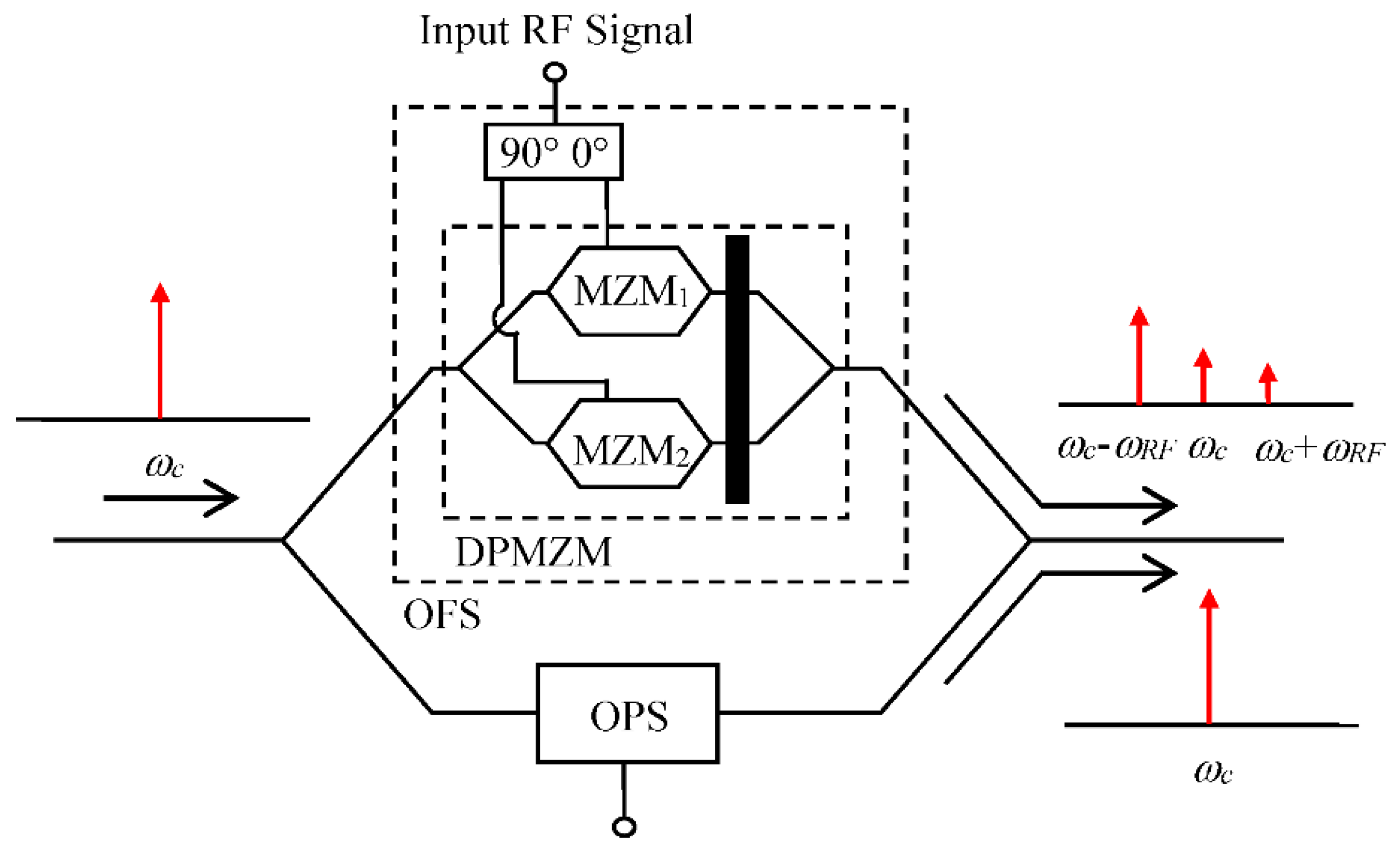
Figure 1 shows the structure of a conventional MPPS formed by an optical frequency shifter (OFS) and an optical phase shifter (OPS) connected in parallel. The OPS shifts the carrier phase. The OFS shifts the carrier frequency by using the single sideband suppressed carrier (SSB-SC) modulation technique to generate only one RF signal modulation sideband with the same frequency as the modulator input RF signal frequency and to eliminate the carrier. The carrier from the OPS beats with the RF signal modulation sideband from the OFS at the photodetector. This generated an RF signal with the same phase shift as the optical phase shift introduced by the OPS. The OFS can be implemented by driving a dual-parallel Mach Zehnder modulator (DPMZM) by a pair of RF signals with 90° phase difference from a 90° hybrid coupler [
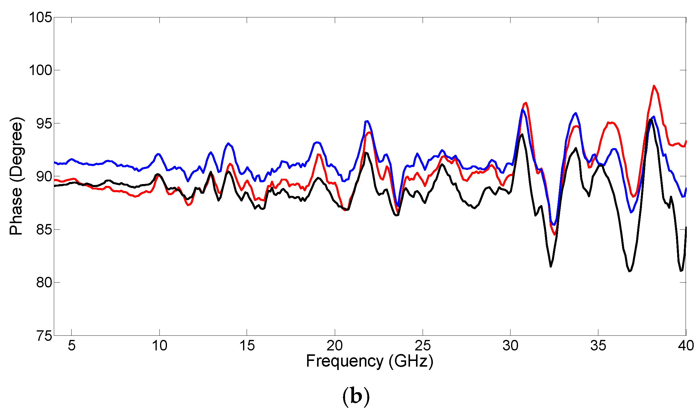
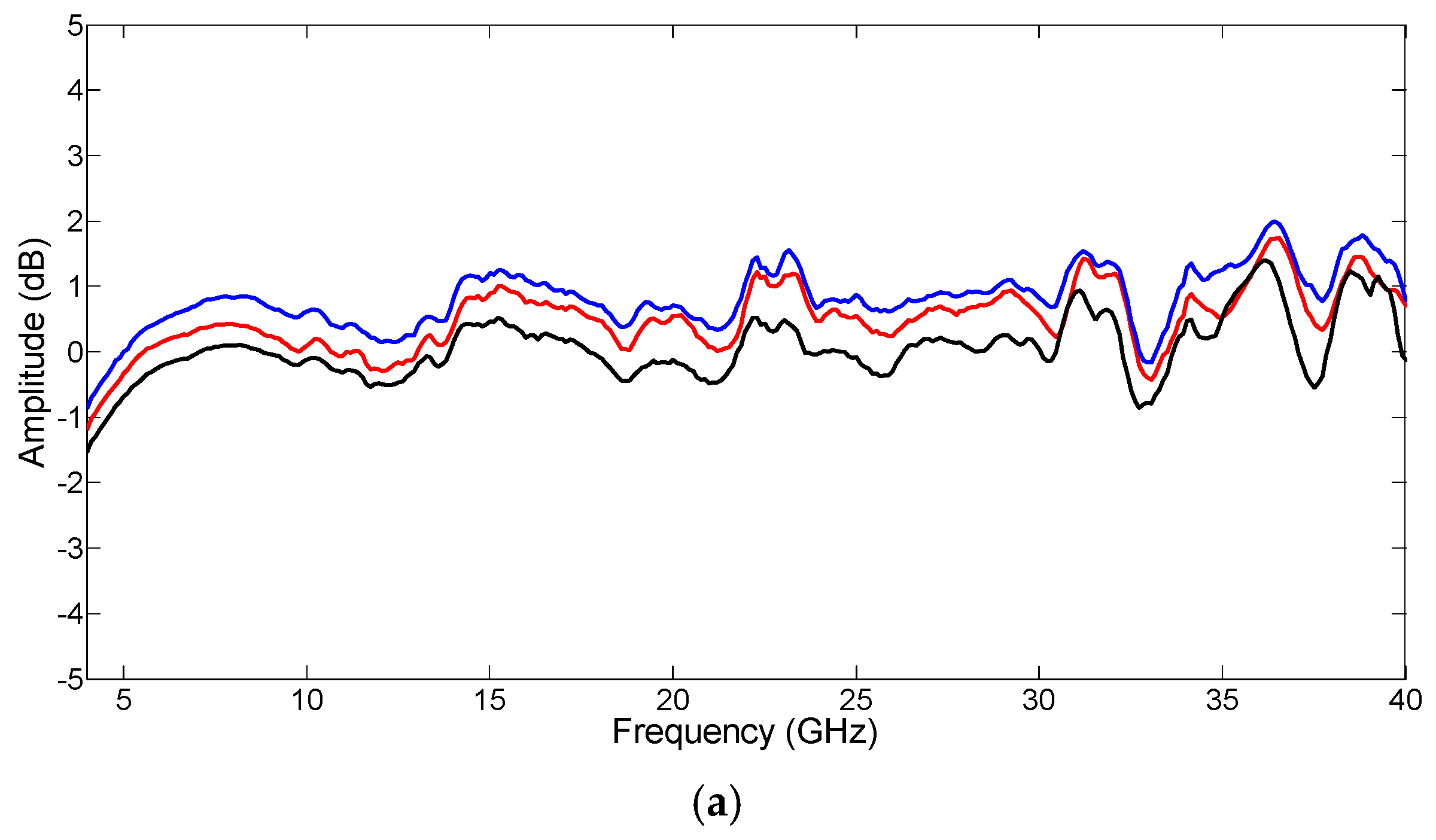
8]. In order for the MPPS to have a wide bandwidth, the 90° hybrid coupler needs to be able to operate over a wide frequency range. Broadband 90° hybrid couplers are commercially available. The frequency responses of three commercial broadband 90° hybrid couplers were measured as shown in
Figure 2. The three couplers were manufactured by Marki Microwave and have the same model number of QH-0440. The operating frequency of the couplers specified in the datasheet is 4–40 GHz.
Figure 2 shows that the maximum amplitude and phase imbalance of the three 90° hybrid couplers are 2 dB and 8.5°, respectively. It can be seen from the figure that large amplitudes and phase imbalances appear at frequencies above 30 GHz. This results in an unwanted RF modulation sideband and a residual carrier at the OFS output, which can be seen from the following analysis.
Referring to
Figure 1, when an RF signal with an angular frequency
ωRF is applied to the OFS, the electric field at the output of MZM
1 and MZM
2 are given by:
where
Ein is the electric field amplitude at the MPPS input,
tff is the insertion loss of MZM
1 and MZM
2,
ki is the optical transmittance for light passing through the
ith arm of the DPMZM,
a1 and
a2 are the modulation index of the top and bottom Mach Zehnder modulator (MZM), respectively,
βbi is the optical phase shift induced by the bias voltage
Vi into MZM
i, and
θ is the phase deviation from 90° of the two RF signals into the DPMZM. MZM
1 and MZM
2 are biased at the null point, i.e.,
βb1 =
βb2 = π/2, and the main MZM of the DPMZM is biased at the quadrature to realize SSB-SC modulation. Neglecting the second and higher order sidebands, the DPMZM output electric field can be written as:
The electric field amplitude of the wanted sideband
Aws, i.e., the frequency shifted light, at an angular frequency
ωc −
ωRF, the unwanted sideband
Auns at ω
c + ω
RF, and the residual carrier
Arc at
ωc at the DPMZM-based OFS output can be obtained from Equation (3) and are given by:
where
LOFS is the OFS insertion loss. In the ideal case,
k1 =
k2 =
k3 =
k4 = 1 and the 90° hybrid coupler has no amplitude and phase imbalance, i.e.,
a1 =
a2 and
θ = 0°, thus the unwanted sideband and the residual carrier are cancelled at the OFS output.
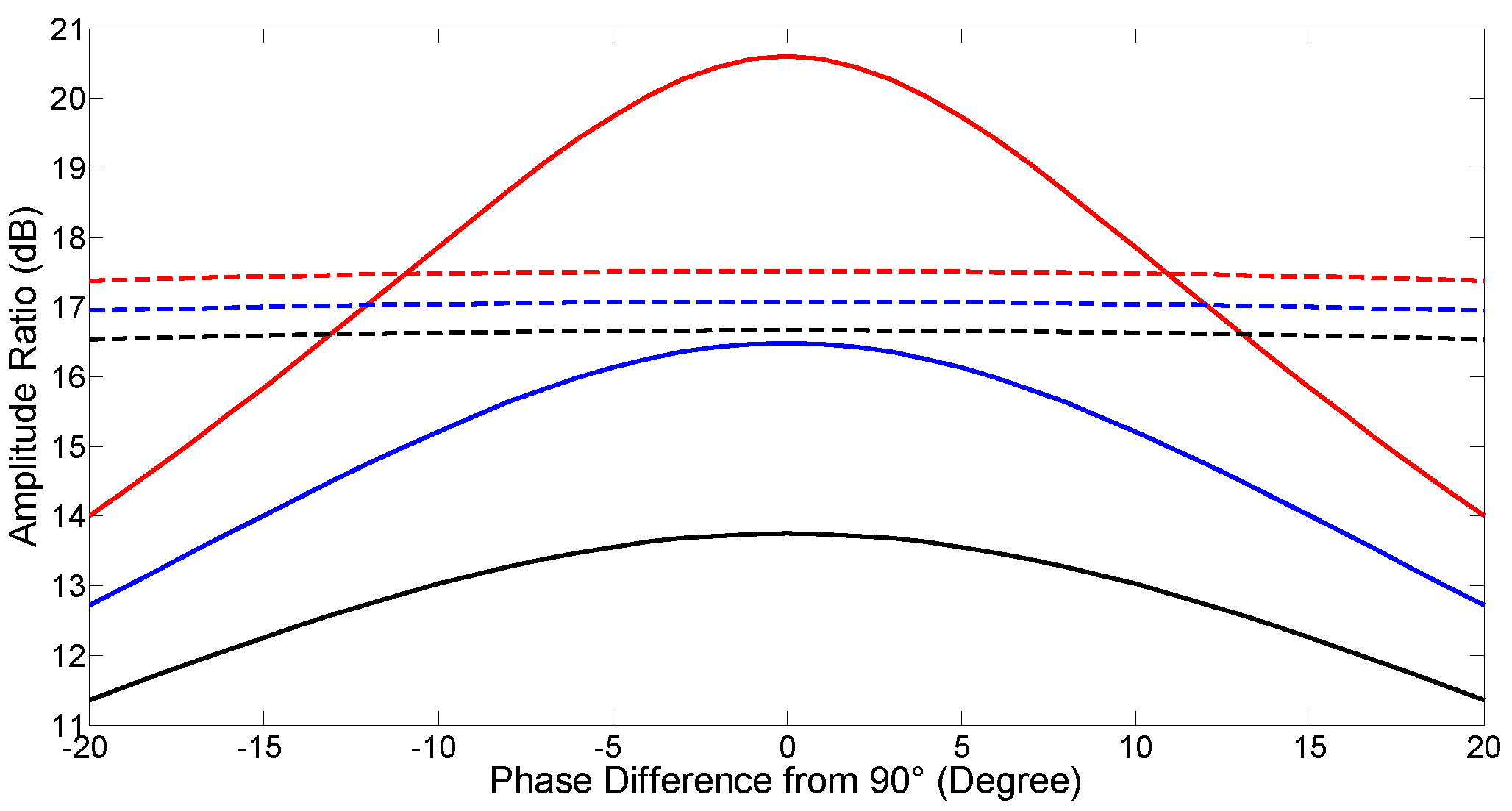
The power of the residual carrier and the unwanted sideband relative to the frequency shifted light power can be obtained from Equations (4)–(6). It can be seen from
Figure 3 that the ratio of the frequency shifted light power to the unwanted sideband power is 15.2 dB and the ratio of the frequency shifted light power to the residual carrier power is 17 dB when the two RF signals into the DPMZM have a ±10° phase difference from 90° and a 2.5 dB power difference. Note that the MPPS in Reference [
5] has an OPS in parallel with the OFS. The OPS only reduces the carrier by around 2 dB due to its insertion loss. Therefore, the residual carrier at the OFS output is much smaller than the carrier at the OPS output. Hence, it has a negligible effect on the MPPS performance. On the other hand, the unwanted sideband cannot be neglected. The OFS- and OPS-based MPPS output electric field with the inclusion of the unwanted sideband at
ωc +
ωRF is given by:
where
LOPS is the OPS insertion loss,
γ = π
VDC/
Vπ is the optical phase shift introduced by the OPS,
VDC is the DC voltage into the OPS,
Vπ is the OPS switching voltage, and
ϕuns and
ϕws are the unwanted and wanted sideband optical phases, respectively. The photocurrent at the RF signal angular frequency
ωRF can be obtained from Equation (7) and is written as:
where ℜ is the photodiode responsivity,
Pin is the optical power into the MPPS, and
φ is the output RF signal phase, which is given by:
It can be seen from Equations (8) and (9) that the MPPS output RF signal amplitude and phase are dependent on
Aws,
Auns,
ϕws, and
ϕuns. The presence of the unwanted sideband with amplitude
Auns and phase
ϕuns is due to the amplitude and phase imbalance of the 90° hybrid coupler used in the MPPS. This shows that the 90° hybrid coupler amplitude and phase imbalance affects the MPPS output RF signal.
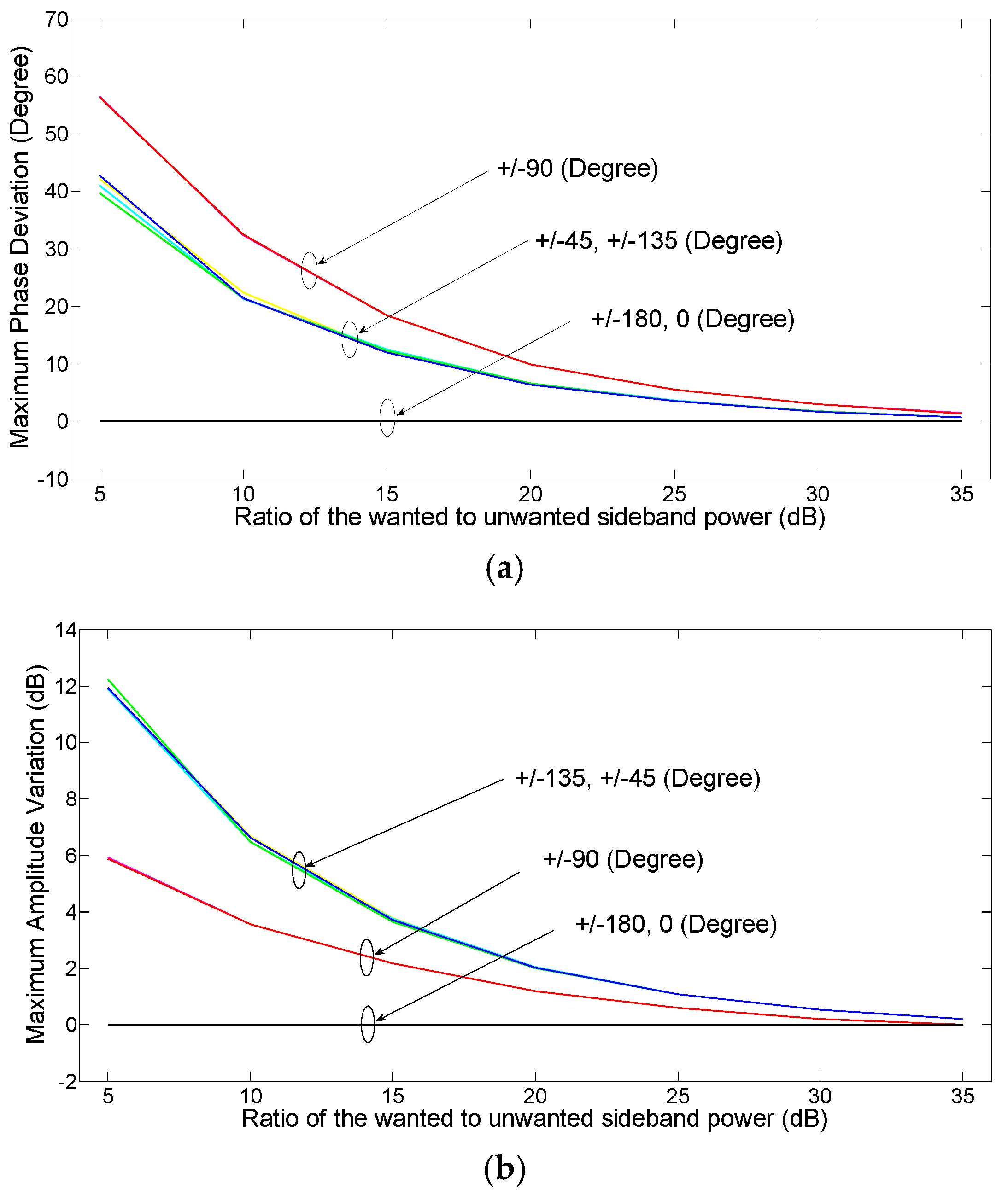
Figure 4 shows the deviation from the desired phase shift and the amplitude variation of the MPPS as a function of the wanted to unwanted sideband power ratio. The figure shows that the amount of MPPS amplitude variation and phase deviation are different for different phase shifts. The ±90° phase shifts have the largest phase deviation, and the ±45° and ±135° phase shifts have the largest amplitude variation. The MPPS has a maximum amplitude variation of 3.8 dB and a maximum phase deviation of ±16° when the unwanted sideband is 15 dB below the wanted sideband. A 90° hybrid coupler with low amplitude and phase imbalance is required to minimize the unwanted sideband amplitude in order to reduce the MPPS amplitude variation and phase deviation. However, such couplers cannot operate in a wide frequency range, which limits the MPPS bandwidth.
Suppressing the unwanted sideband can reduce the MPPS amplitude variation and phase deviation, which can be achieved by inserting an optical filter at the optical modulator output. Since the unwanted sideband has a high amplitude only at the frequencies far away from the optical carrier due to the 90° hybrid coupler has large amplitudes and phase imbalances at high frequencies as shown in
Figure 2, an expensive sharp edge roll-off optical filter is not required to suppress this unwanted sideband. The optical filter is designed to pass the wanted sideband from the OFS and the carrier from the OPS but suppress the unwanted sideband at high frequencies, e.g., >30 GHz. Such filters can be implemented by using autoregressive ring lattice architecture in planar waveguides [
9] or by designing the reflection spectra of a fiber Bragg grating [
10].
The loss of the OFS and OPS-based MPPS, which is defined as the ratio of the photodetector output RF signal power to the RF signal power into the MPPS, was simulated using VPITransmissionMaker photonic simulation software. The simulation results show that the MPPS has an 8.3 dB extra loss compared with a conventional fiber optic link, which is formed by a laser source, a quadrature-biased MZM, and a photodetector, when the two systems have the same 7 dBm average optical power into the photodetector. This extra 8.3 dB loss is mainly due to the removal of one RF modulation sideband in the phase shifter structure. In general, MPPSs have a higher loss, which leads to a higher noise figure, than conventional microwave phase shifters. However, MPPSs are capable of realizing a continuous 0–360° phase shift while keeping the RF signal amplitude constant over a very wide frequency range that cannot be achieved by its electronic counterpart. The spurious free dynamic range (SFDR) of the MPPS and the conventional fiber optic link were also simulated by applying two RF signals with the frequencies of 10 GHz and 10.1 GHz into the modulator and measuring the output RF signal power at 10 GHz (or 10.1 GHz) and the third order intermodulation distortion component power at 9.9 GHz (or 10.2 GHz). The simulation results show that the two systems have a similar SFDR of around 100 dB Hz2/3 when they have a shot noise limited performance with a noise floor of −161 dBm/Hz. However, in practice, an optical amplifier is required in the MPPS to compensate for the insertion loss of the integrated OFS and OPS structure, which is higher than the insertion loss of an MZM used in a fiber optic link. The use of an optical amplifier in the OFS and OPS-based MPPS introduces the signal-spontaneous beat noise, which is above the shot noise and is the dominant noise source in the system. This degrades the phase shifter dynamic range performance. A low insertion loss integrated OFS and OPS structures, and a low noise figure optical amplifier are required to minimize the degradation of the phase shifter dynamic range performance.
3. Experimental Results
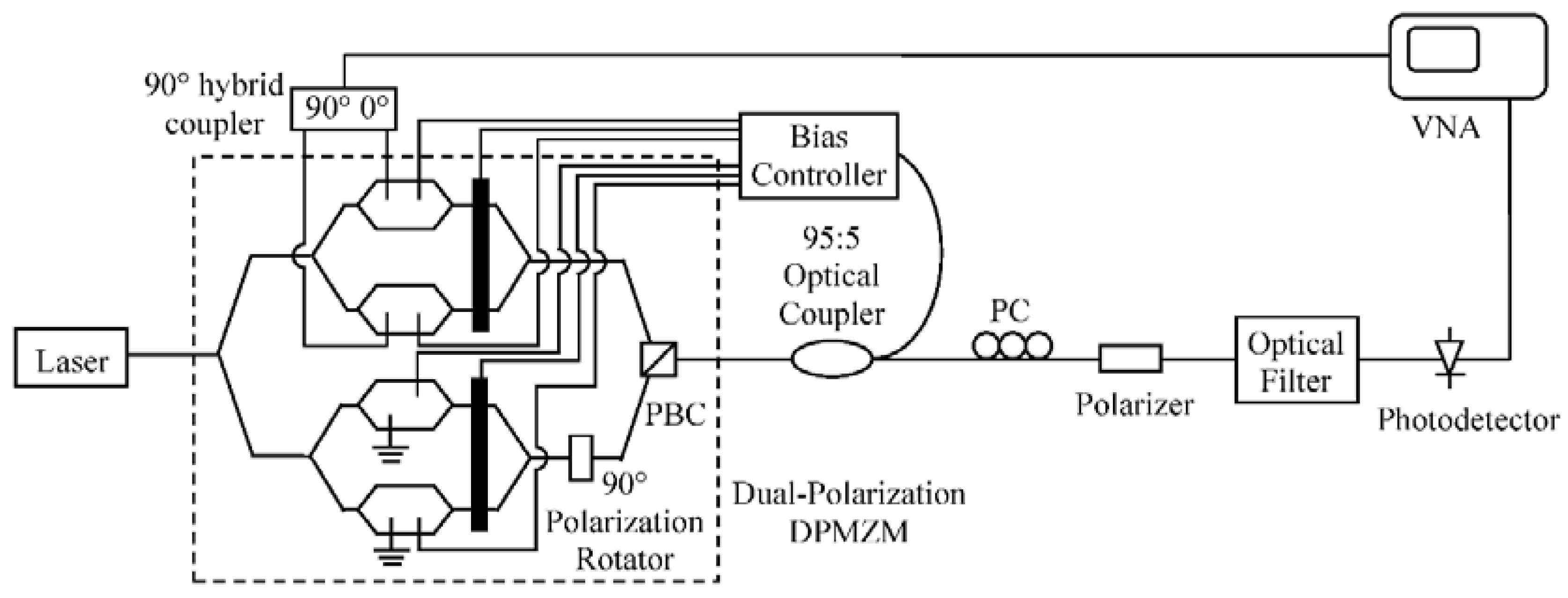
Experiments were set up to investigate the ripples in the frequency response of a MPPS and to verify that using a low cost optical filter can improve MPPS frequency response performance. The experimental setup is shown in
Figure 5. The laser source (Keysight N7714A) was a wavelength tunable laser operated at 1557.8 nm. The laser output power was 16 dBm. A dual-polarization DPMZM was connected after the laser source. It was formed by two DPMZMs, a 90° polarization rotator, and a polarization beam combiner (PBC). Each DPMZM consisted of two MZMs connected in parallel and an OPS at one of the MZM outputs. No RF signal was applied to the lower DPMZM, and the two MZMs were biased at the maximum and minimum transmission point, respectively. Therefore, the optical carrier passed through only one MZM but was blocked by the other MZM. Thus, by controlling the voltage into the OPS, the optical carrier phase could be tuned. The upper DPMZM was driven by a pair of RF signals with 90° phase difference via a 4–40 GHz bandwidth 90° hybrid coupler (Marki Microwave QH-0440 [
11]) with the frequency response shown in
Figure 2 (red line). A SSB-SC RF modulated optical signal could be generated by designing the bias voltages into the upper DPMZM [
8]. Therefore, the dual-polarization DPMZM had the same function as an integrated OFS and OPS structure. A single compact modulator bias controller (PlugTech MBC-DPIQ-01 [
12]) was used to control the modulator bias voltages. A polarization controller (PC) and a polarizer at the output of the dual-polarization DPMZM were employed to ensure the carrier and the sideband had the same polarization state. This was followed by an optical filter, which had 1.5 dB insertion loss. Since the laser source had high output optical power and the optical filter had low insertion loss, the average optical power after the optical filter was −4 dBm. No optical amplifier was used in the experiment. The carrier with a tunable optical phase shift from the lower DPMZM and the single RF modulation sideband from the upper DPMZM beat at a 50 GHz bandwidth photodetector (U2t XPDV2120R), which was connected to a 43.5 GHz bandwidth vector network analyzer (VNA) (Agilent N5224A) to display the phase shifter amplitude and phase response.
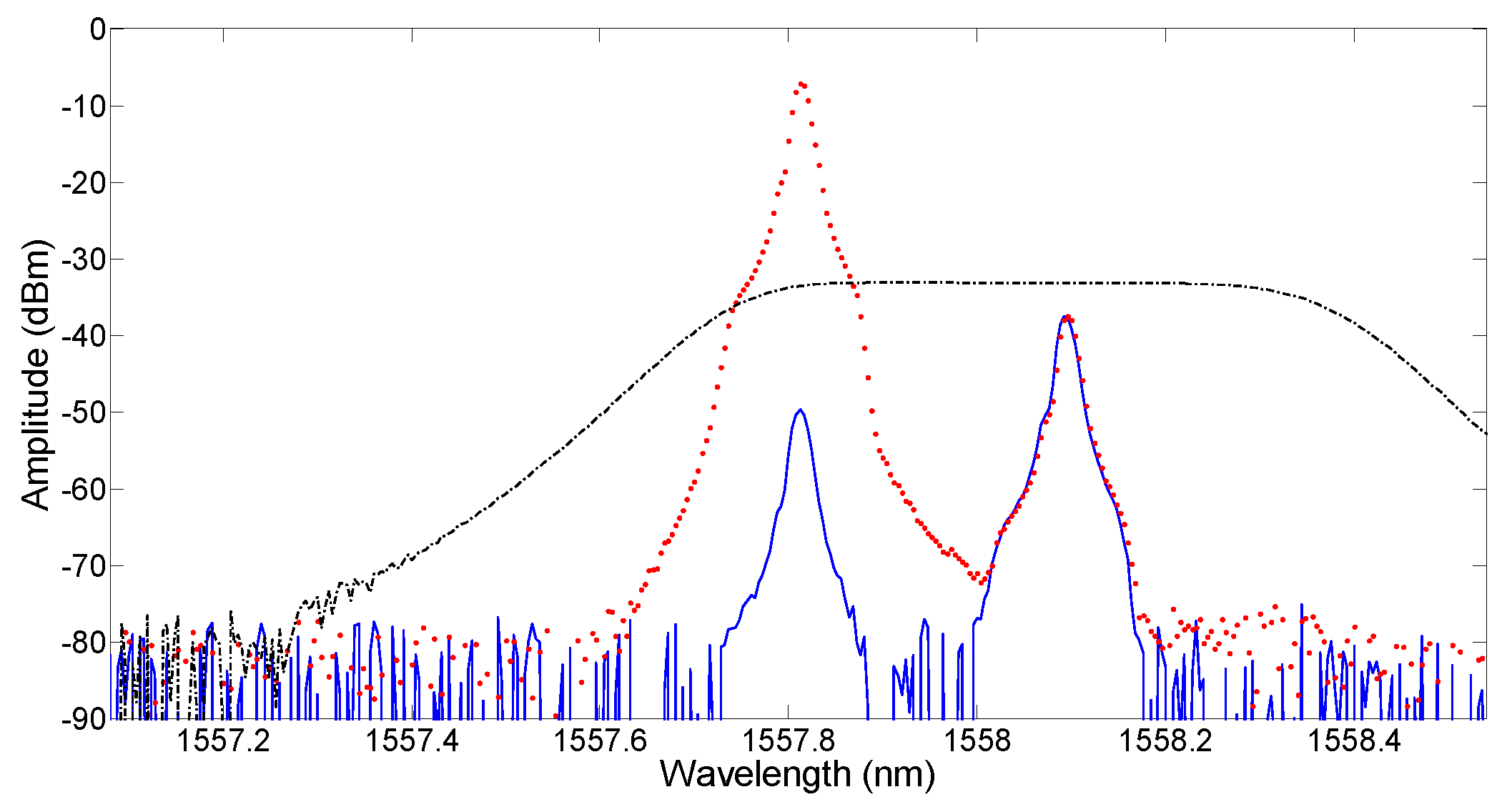
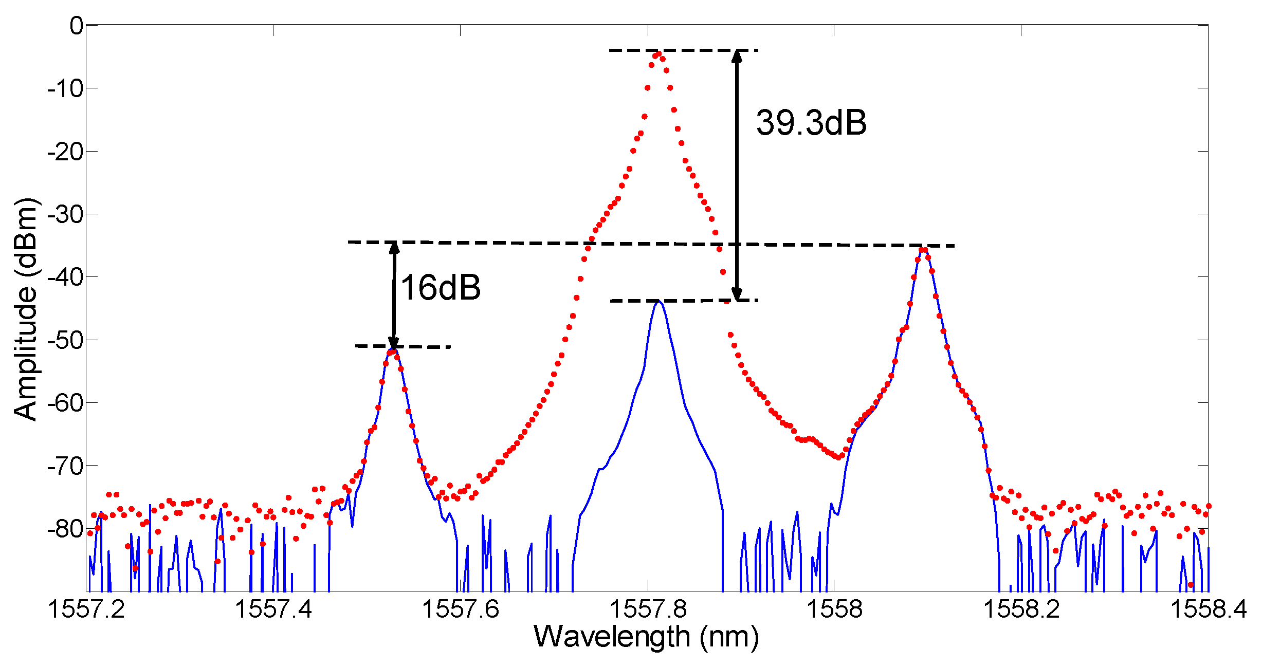
The optical spectrum at the output of the dual-polarization DPMZM was measured on an optical spectrum analyzer (OSA), as shown in
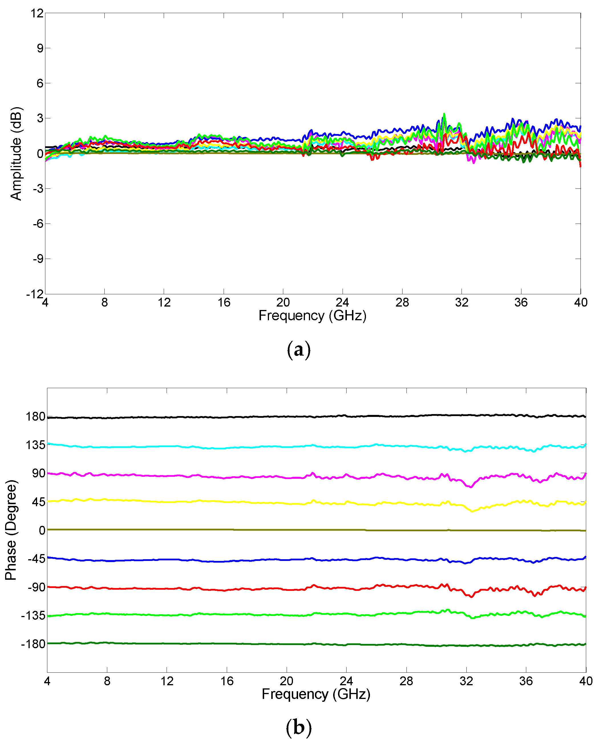
Figure 6, when the upper DPMZM was driven by a 32 GHz RF signal. This shows that, for a high input RF signal frequency of 32 GHz, the unwanted left sideband was only 16 dB below the wanted right sideband due to the 90° hybrid coupler had large amplitudes and phase imbalances at high frequencies. Note that even though the carrier at the output of the upper DPMZM could not be fully suppressed, the residual carrier was 39.3 dB below the carrier from the lower DPMZM. Therefore, the residual carrier had a negligible effect on the MPPS performance. The amplitude and phase response of the MPPS were first measured without an optical filter and the results are shown in
Figure 7. This was done by programming the bias controller to alter the DC voltage into the OPS inside the lower DPMZM in the dual-polarization DPMZM. The experimental results show there are 4.2 dB amplitude variations and a ±12° phase deviation for a −180° to 180° phase shift over the 4 to 40 GHz frequency range. Note that the amount of MPPS amplitude variation and phase deviation were different for different phase shifts. It can be seen from the figure that ±45° phase shifts have large amplitude variations and ±90° phase shifts have large phase deviations, which are consistent with the simulation results given in
Figure 4.
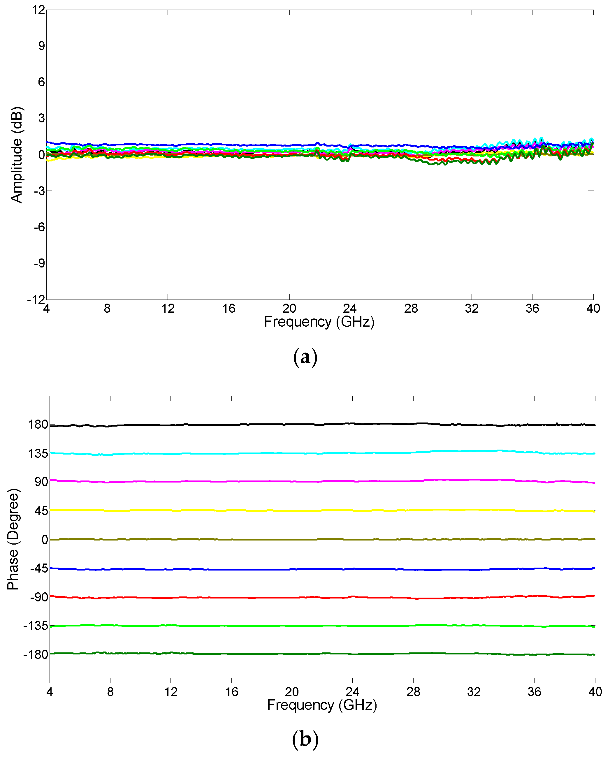
An optical filter with an optical spectrum as shown in
Figure 8 was connected after the polarizer to suppress the unwanted sideband. It had a center wavelength of 1558.05 nm, and a −3 dB and −20 dB bandwidth of 0.62 nm and 1.03 nm, respectively. Its roll-off factor was around 83 dB/nm (0.67 dB/GHz). The optical filter passed both the optical carrier and the wanted right sideband but suppressed the unwanted left sideband, especially at the frequencies far away from the optical carrier.
Figure 8 shows that the unwanted left sideband at the frequency of 32 GHz away from the optical carrier was suppressed to the OSA noise level. Therefore, a single sideband RF modulated optical signal with large unwanted sideband suppression can be obtained not only for low RF signal frequencies but also for high RF signal frequencies. The measured amplitude and phase response of the MPPS with the inclusion of an optical filter are shown in
Figure 9. It can be seen from the figure that the MPPS exhibits a flat amplitude and phase response performance over a wide bandwidth from 4 to 40 GHz. The amplitude variation was <2.2 dB and the phase deviation was <±3.8° for a −180° to 180° phase shift over the MPPS bandwidth. Similar amounts of amplitude variation and phase deviation in the phase shifter frequency response were obtained when the 90° hybrid coupler used in the experiment was replaced with the other two 90° hybrid couplers with the frequency responses shown in
Figure 2. These small amplitude variations and phase deviations are due to the residual carrier at the output of the OFS and the noise present in the system. Nevertheless, the experimental results verify the concept of inserting a low cost optical filter in a MPPS implemented using a 90° hybrid coupler can overcome the amplitude variation and phase deviation problem caused by the 90° hybrid coupler amplitude and phase imbalance.

 ,
, 