Abstract
Printed Circuit Board (PCB) defect detection is critical for quality control in electronics manufacturing. Traditional manual inspection and classical Automated Optical Inspection (AOI) methods face challenges in speed, consistency, and flexibility. This paper proposes a CNN-based approach for automatic PCB defect detection using the YOLOv5 model. The method leverages a Convolutional Neural Network to identify various PCB defect types (e.g., open circuits, short circuits, and missing holes) from board images. In this study, a model was trained on a PCB image dataset with detailed annotations. Data augmentation techniques, such as sharpening and noise filtering, were applied to improve robustness. The experimental results showed that the proposed approach could locate and classify multiple defect types on PCBs, with overall detection precision and recall above 90% and 91%, respectively, enabling reliable automated inspection. A brief comparison with the latest YOLOv8 model is also presented, showing that the proposed CNN-based detector offers competitive performance. This study shows that deep learning-based defect detection can improve the PCB inspection efficiency and accuracy significantly, paving the way for intelligent manufacturing and quality assurance in PCB production. From a sensing perspective, we frame the system around an industrial RGB camera and controlled illumination, emphasizing how imaging-sensor choices and settings shape defect visibility and model robustness, and sketching future sensor-fusion directions.
1. Introduction
Quality inspection of Printed Circuit Boards is a vital step in electronics manufacturing because PCB defects can lead to malfunctions or reliability issues in electronic devices [1]. PCBs may suffer from a range of defects introduced during fabrication, which can be classified into functional defects (affecting the electrical performance) and cosmetic or surface defects (affecting appearance). Common PCB defect types include open circuits, short circuits, missing holes (plating voids), mouse bites (notches in traces), spurs (protruding copper), and spurious copper left over on the board [2]. Traditionally, PCB inspections have relied on human visual inspections and dedicated equipment, such as in-circuit testing and Automated Optical Inspection (AOI) systems. Nevertheless, manual inspections are labor-intensive, error-prone, and inefficient, while AOI systems based on classical image processing face limitations in adapting to new defect types and variations in lighting or board design [2]. These challenges drive the need for more flexible and intelligent defect detection methods. In recent years, deep learning, especially Convolutional Neural Networks (CNNs), has revolutionized computer vision, achieving superior performance in image classification and object detection tasks [3]. CNN-based models can automatically learn rich feature representations from raw images [4], making them well-suited for identifying the subtle patterns of PCB defects. Object detection algorithms, such as the You Only Look Once (YOLO) family, have shown high accuracy and real-time speed. Recently, advanced methods such as SGT-YOLO [5] and YOLO-SSW [6] have been proposed to further improve detection performance on PCB surfaces. This capability makes YOLO and similar models attractive for PCB inspection, where speed and accuracy are essential.
Researchers have started applying deep learning to PCB defect inspections with promising results. For example, Ding et al. developed a tiny defect detection network (TDD-Net) based on Faster R-CNN to detect minor PCB defects [7]. Hu and Wang improved a Faster R-CNN model with feature pyramids for better accuracy [8]. More recently, one-stage detectors have gained traction. Chen et al. introduced a Transformer-YOLO model for PCB defects, incorporating attention mechanisms to refine the predictions from YOLO [9]. In contrast, Liu and Wen [10] and Liao [11] et al. proposed lightweight YOLO-based networks (using MobileNet backbones and other enhancements) for real-time PCB surface defect detection. These deep learning approaches outperformed traditional methods in accuracy and adaptability.
In the domain of PCB assembly inspection, Shen et al. presented a YOLOv5-based model (PCBA-YOLO) and achieved more than 97% mean average precision on an assembled PCB defect dataset [12]. Similarly, for bare PCB surfaces, Xiao et al. reported a mAP above 98% by improving a YOLOv7-tiny model with attention and other modules [13]. Additionally, Zhang and Li introduced SMA-YOLO, a lightweight algorithm employing Shannon entropy to optimize small object detection [14]. Such studies suggest the promising role of CNN-based detection for PCB quality inspection. This paper proposes a new algorithm-guided defect detection on PCB inspection via CNN combined with a YOLO style one-stage detector. The proposed solution was developed to detect and categorize various PCB failure modes automatically. The model was trained and tested over a dataset containing PCB images annotated with defect labels. This method was evaluated in terms of the detection accuracy and speed, compared to the state-of-the-art YOLOv8 model, to determine the effectiveness of the model.
We propose an inline-oriented, sensor/illumination-aware detection pipeline built on YOLOv5 and systematically quantify how sensing/lighting ↔ augmentation ↔ detection performance interact under production constraints.
On a 19-class, in-production dataset, we report per-class AP/Precision/Recall and COCO-style mAP@[0.5:0.95], providing a reproducible baseline for PCB AOI.
Through system-level analysis spanning YOLOv5/YOLOv8, augmentation variants, and edge deployment (T4), we deliver quantitative design guidelines (accuracy–speed–parameters) for real-time inline use.
2. Theoretical Framework and Algorithmic Dynamics
2.1. Data-Centric Algorithmic Challenges and Manifold Complexity
The primary scientific challenge addressed in this work is not merely the application of deep learning to a new dataset, but the resolution of the “Curse of Dimensionality” and feature ambiguity inherent to high-cardinality industrial distributions. The recent literature emphasizes that domain-specific data characteristics—such as extreme scale variation or background complexity—function as critical boundary conditions that necessitate architectural innovation. For instance, Zhang and Li [14] proposed the SMA-YOLO framework to address the specific entropy distribution of small objects in UAV imagery, demonstrating that rigorous analysis of data-specific constraints (e.g., small targets in complex backgrounds) is a prerequisite for advancing detection theory. Paralleling the scientific logic of [14], we posit that the 19-class PCB defect taxonomy presents a distinct topological challenge: significant semantic ambiguity among morphologically similar defects. Standard benchmarks often separate orthogonal classes (e.g., dog vs. cat), whereas our industrial domain involves distinguishing dent from dent/short, or unetched from spurious copper within a highly correlated feature space. Mathematically, as the number of classes increases to 19, the decision boundaries in the latent feature space become densely populated and highly non-linear. Consequently, the probability of feature overlap between inter-class samples increases, creating a risk where the network converges to local minima that ignore subtle fine-grained details. To scientifically address this—and following the methodology of maximizing feature interaction for specific domains as seen in [14]—we leverage a framework governed by Gradient Flow Optimization and Photometric Manifold Alignment. This design is explicitly intended to maximize inter-class variance, even when defect scales are microscopic (as small as 3 × 3 pixels), ensuring that the model solves the specific manifold crowding problem of this industrial distribution.
Unlike conventional studies that validate detection algorithms on standard benchmarks with limited defect categories (typically 6 classes), this study addresses a complex taxonomy of 19 distinct defect classes. This transition from low-cardinality to high-cardinality classification fundamentally alters the learning dynamics of the neural network. Consequently, our methodology is not merely an application of existing tools but a scientifically grounded framework designed to solve the specific problems of gradient flow stagnation and manifold crowding inherent to high-dimensional industrial data.
2.2. Gradient Flow Optimization via CSP Architecture
To resolve the 19-class topology without vanishing gradients, we employ a Cross-Stage Partial (CSP) network backbone. The selection of CSP is motivated by its ability to optimize gradient flow dynamics. In a deep convolutional network, redundant gradient information often accumulates as it propagates through repetitive texture layers (such as the PCB substrate). The CSP architecture mathematically addresses this by partitioning the feature map of the base layer x into two distinct gradient paths, x = [x′, x″]. The Metric Path (x′): Bypasses the dense block via a direct skip connection. The Computational Path (x″): Undergoes dense convolution operations F(x″). The final output is formed by concatenating these paths: y = x′ + F(x″). Theoretically, this mechanism truncates the redundant gradient flow during backpropagation. By preventing the network from updating weights based on redundant background information, we force the optimization landscape to focus on the high-frequency gradients associated with defect boundaries. This ensures that the feature extractor learns robust morphological representations for all 19 classes rather than overfitting to the board texture.
2.3. Photometric Manifold Alignment
Industrial imaging is subject to Covariate Shift caused by stochastic variations in illumination and sensor noise. We formulate data augmentation not as a heuristic for increasing dataset size, but as a rigorous process of Photometric Manifold Alignment. We apply Contrast Limited Adaptive Histogram Equalization (CLAHE) to locally maximize the entropy of defect features. By redistributing the pixel intensity probability density function (PDF) within local tiles and applying a clip limit β, we mathematically constrain the amplification of sensor noise in the homogeneous substrate regions:
Furthermore, Gamma Correction ( = ) is applied as a non-linear mapping to expand the dynamic range of shadowed regions (e.g., spaces between traces). This aligns the input data manifold with the network’s initialization assumptions, ensuring that valid gradient signals can be generated even from low-contrast defects like oxidation or shallow dents.
2.4. Training and Evaluation Protocol
We train and validate on the same acquisition setup as testing. Metrics include Precision/Recall, mAP@0.5, and COCO-style mAP@[0.5:0.95] (IoU ∈ {0.50…0.95} in 0.05 steps; 101-point interpolation; macro-averaged) [15,16]. Runtime is measured under batch-1, 640 × 640, with NMS and warm-up. On RTX 4090 (NVIDIA Corporation, Santa Clara, CA, USA; PyTorch v2.4.1, no visualization), the baseline reaches 118.1 FPS; edge deployment uses TensorRT v10.4.0 (FP16/INT8) on an NVIDIA T4(NVIDIA Corporation, Santa Clara, CA, USA), with throughput, average power, and J/frame reported in Section 5.
2.5. Position in the Literature
To situate the proposed framework within the existing PCB AOI literature, we compare it with several representative CNN-based approaches in Table 1. The table summarizes differences in task setup, datasets, metrics, and deployment focus.

Table 1.
Comparison between representative PCB defect detection studies and this work.
As summarized in Table 1, prior work mainly focuses on model-level improvements (e.g., Faster R-CNN variants, Transformer-enhanced YOLO, lightweight YOLO versions) on bare-board or PCBA datasets, often reporting only mAP@0.5 and without a unified edge-deployment protocol. In contrast, our study provides an inline-oriented, sensor/illumination-aware framework with a 19-class in-production benchmark and edge validation, which addresses a methodological gap between academic PCB AOI research and industrial inline requirements.
3. Experiments
3.1. Dataset
A dataset of PCB images with labeled defects was prepared to evaluate the proposed defect detection algorithm. The dataset consisted of 1254 (expanded from 209 original images) high-resolution PCB images annotated with multiple defect categories. The dataset consisted of high-resolution images of PCB panels collected from in-house PCB panels under controlled RGB illumination (provider-restricted); see the Data Availability Statement for access conditions. All 209 original captures (Figure 1) originate from a single PCB layout produced on one manufacturing line under controlled RGB illumination; therefore, the reported results characterize within-layout performance. Cross-layout generalization is outside the present scope and is discussed in Section 5. This study considered a range of defect types commonly encountered in PCB fabrication, including the following: bridging, crease, dent, dent/short, double_processing, excess_copper, high_resistance_all, hole_eccentricity, hole_misalignment, open, oxidation, short, short/excess_copper, short/unetched/dent, slit, through_hole, unetched, unetched/short, and vibration.
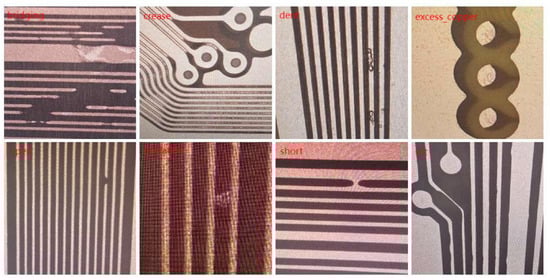
Figure 1.
Original images.
3.1.1. Data Augmentation
To address limited training data and improve robustness to photometric/sensor variations and subtle defect textures [17,18,19,20], we adopt a controlled augmentation pipeline. Starting from 209 raw PCB images, we generate an additional 1045 augmented images, yielding 1254 training samples in total (6×). The pipeline includes (i) gamma correction and log transform to redistribute luminance and enhance low-intensity contrast (SNR/CNR) [18]; (ii) CLAHE (tile 8 × 8, clip limit [2,4]) to increase local contrast while preserving material cues [17]; (iii) mild blur/sharpen (Gaussianσ ∈ [0.6, 1.2] or unsharp-mask amount ∈ [0.5, 1.0]) to model slight defocus and emphasize fine edges [18]; and (iv) small geometric transforms (±5–10° rotations; horizontal/vertical flips with p = 0.5) that do not alter board topology [21].
Each transform is applied with probability p ∈ [0.3, 0.7], and parameters are sampled uniformly from the specified ranges. Augmentations are applied only during training; validation and test images remain unchanged. Representative examples are shown in Figure 2.
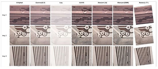
Figure 2.
Augmentation exemplars on three representative PCB images (rows: Img 1–Img 3). From left to right: Original, Gamma (0.7), Log, CLAHE (tile 8 × 8, clip = 3.0), Blur (σ = 1.0), Sharpen (USM), Rotate (+7°).
Using these algorithms, the brightness is re-allocated to compress the dynamic range. In contrast to the traditional data-augmentation, which is only approximately rotation and flipping, noise randomness is suppressed, and SNR/CNR are increased. It also increases the perceived sharpness and local contrast because the edges and textures are exaggerated. This greatly increases the detection robustness and accuracy (and hence segmentation) in low-light, noisy, and somewhat blurred environments [15]. Note that rotation and flipping do not improve the quality of the pixels themselves or hold more information, which is significant in terms of image enhancement.
3.1.2. Data Tagging
All defect instances in the images were annotated with LabelImg and assigned a defect category label. In total, the dataset contained 1254 PCB images, which we split into training, validation, and test subsets (approximately 80%, 10%, and 10%, respectively). These images cover the aforementioned defect types as distinct classes, along with representative non-defective samples for background. Figure 3 presents sample PCB images with various defect annotations. The figure shows example PCB images from the dataset containing solder-bridge (“bridging”) defects; ground-truth bounding boxes indicate the defect locations and labels.
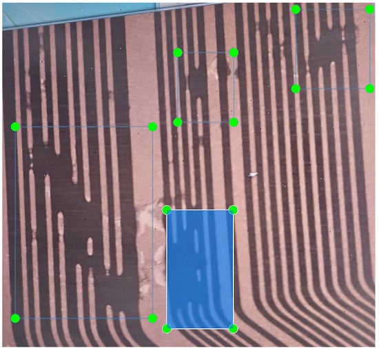
Figure 3.
PCB image with solder-bridge (“bridging”) defects annotated in a labeling tool. Blue boxes denote ground-truth bounding boxes; green dots are auxiliary point annotations used for alignment/inspection.
Figure 4 presents the Visual Bounding Box Overlay Annotation schema in YOLO format output by the LabelImg tool, which consists of five normalized elements: [class_id] [x_center] [y_center] [width] [height].
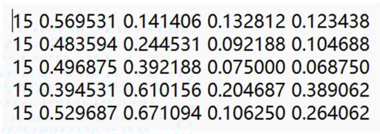
Figure 4.
YOLO Annotation Format.
The scheme provides a neat localization and classification of PCB defects. The bounding box visual overlays on the PCB images are provided in Figure 3. These annotations serve as ground truth by accurately drawing the boundaries on defect regions, making them ideal for supervised learning and validation.
Dataset Card. Provenance: in-house PCB panels under controlled RGB illumination (provider-restricted). Taxonomy: 19 classes (bridging, crease, dent, dent/short, double_processing, excess_copper, high_resistance_all, hole_eccentricity, hole_misalignment, open, oxidation, short, short/excess_copper, short/unetched/dent, slit, through_hole, unetched, unetched/short, vibration). Split: 80% train/10% validation/10% test. Resolution: high-resolution boards; smallest defects span ≥ 2–3 pixels across the narrow dimension. Annotation: YOLO box format [cls x y w h] (normalized), double-pass QA. Formats: images (PNG/JPEG), labels (YOLO txt), class list (data/pcb.yaml).
3.2. Model and Training
We adopted a single-stage CNN detector based on YOLOv5s (PyTorch implementation). The network follows the standard YOLO design with a CSP-based backbone for feature extraction, a PANet/FPN neck for multi-scale fusion, and three detection heads for different spatial scales. To cope with limited labeled data, the model is initialized from COCO pre-trained weights and the output layer is resized to our defect classes (as specified in data/pcb.yaml). The final model has ≈7.5 M parameters and is lightweight enough for real-time deployment of our target hardware.
Model Architecture. The detector follows YOLOv5s: a CSP-style backbone (C3 blocks) extracts features at strides {8, 16, 32}; a PANet/FPN neck fuses multi-scale features (P3/P4/P5); and a decoupled detection head performs class logits and box regression at three scales. With 19 classes and 640 × 640 input, the model has ≈7.5 M parameters and runs at ~118.1 FPS on RTX 4090 (batch = 1), including NMS. We initialize from COCO weights and resize the output head to 19 classes. A summary is provided in Table 2.
Table 2.
Model configuration and hyperparameters (ready-to-run).
We start with 209 raw PCB images and generate 1045 augmented samples for a total of 1254 images (6×). The augmentation pipeline includes gamma correction, logarithmic transform, CLAHE, mild blur/sharpening, and small geometric perturbations (random rotation/translation). Augmentations are only applied to the training split; validation/test splits remain unchanged.
Training setup: We train YOLOv5s at 640 × 640 with batch size 8 for 200 epochs using Ultralytics’ auto optimizer selection. Early stopping is applied with patience = 10 based on validation mAP@0.5. For reproducibility, we release the exact commands, data/pcb.yaml (paths, class names), and the trained checkpoint, as summarized in Table 3.
Table 3.
Operation steps and commands (ready-to-run).
We report Precision, Recall, and mAP@0.5 on the held-out test split. A separate 10% validation set is used only for early stopping and hyper-parameter tuning. Deployment thresholds are conf = 0.25 and IoU = 0.45.
Protocol Clarification Note. To avoid ambiguity, we clarify that the reported results are obtained from a fixed 80%/10%/10% train/validation/test split; hyperparameters were fixed a priori (YOLOv5 defaults consistent with prior PCB literature).
4. Results
After training, the defect detection model was evaluated on the held-out test set of PCB images. The performance was quantified using standard object detection metrics: precision, recall, and mean average precision (mAP). The precision measures how many of the defects detected by the model are true defects (versus false alarms), while recall measures how many of the true defects present were successfully detected. The mAP@0.5 (mean AP at 50% IoU threshold) provides an overall measure of the detection accuracy across all classes.
TP (True Positives): Number of correctly predicted bounding boxes.
- FP (False Positives): Number of predicted boxes that do not correspond to any actual object.
- : Average Precision for the class
- N: Total number of classes
On the held-out test split, our YOLOv5s-based detector achieved Precision = 0.9058, Recall = 0.9124, and mAP@0.5 = 0.9069. These metrics indicate that the detector covers most defect instances while maintaining a low false-positive rate. Per-class AP values were all ≥0.89 (see Table 4), and we follow common object-detection practice by reporting Precision/Recall and mAP@0.5 (area under the PR curve at IoU = 0.5) [16,17,18,21,22,23]. The single Precision/Recall values we report correspond to the deployment operating point (conf = 0.25, IoU = 0.45).
Table 4.
Per-class AP on the test set (conf = 0.25, IoU = 0.45).
Traditional Automated Optical Inspection (AOI) systems can suffer from missed defects or high false-call rates when illumination or board layout is challenging. Under the same imaging setup, our deep model demonstrates improved defect coverage compared with representative AOI methods reported in the literature [1].
Beyond mAP@0.5, we report per-class Precision/Recall at the deployment operating point (conf = 0.25, IoU-NMS = 0.45). The weakest categories are short/unetched/dent, hole_eccentricity, and hole_misalignment, consistent with their tiny size and visual similarity, and thus they are prioritized for future data collection and tuning. To further analyze the specific misclassifications, Figure 5 illustrates the confusion matrix normalized by the true class.
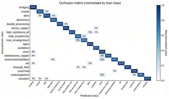
Figure 5.
Confusion matrix (normalized by true class).
To isolate the contribution of training-time augmentation under our fixed protocol, we compare No Augmentation, HSV + Flip, and the YOLOv5-default pipeline at 640 × 640 with identical optimizer/schedule and seed (see augmentation definitions in Section 3.1.1). Table 5 summarizes the quantitative impact of data augmentation on mAP@0.5, Precision, and Recall.
Table 5.
Impact of data augmentation on mAP@0.5/Precision/Recall.
Figure 6 and Figure 7 illustrate detections on test-set PCB images. The model correctly locates and classifies multiple defects in a single image—for example, an open circuit (trace break), a solder short (bridge between adjacent lines), and fine residual copper specks. Predicted boxes align closely with the annotated regions, supporting the aggregate metrics and highlighting the system’s practicality for inline flagging and repair.
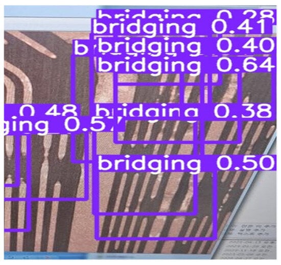
Figure 6.
Detection Result for the “bridging” Defect.
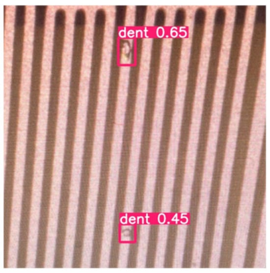
Figure 7.
Detection Result for the “dent” Defect.
Comparison with YOLOv8s (same protocol). Under identical 640 × 640 training and the same 80/10/10 split and inference thresholds, YOLOv8s attained a higher mAP@0.5 = 0.9518 than YOLOv5s (0.9069), with Precision 0.9512 vs. 0.9058 and Recall 0.9527 vs. 0.9124. YOLOv5s remained smaller and marginally faster in our setup (v5 ≈ 7.2 M params; v8 ≈ 11.2 M params). However, YOLOv5s remained marginally faster and smaller on our RTX 4090 (118.1 FPS, ~7.5 M parameters) than YOLOv8s (68.1 FPS, 11.2 M), which motivated our choice of YOLOv5s for real-time inline inspection. Architectural differences behind YOLOv8’s gains (e.g., an anchor-free, decoupled head and updated C2f backbone/neck) are documented in the Ultralytics technical notes [24].
Unless otherwise stated, metrics are computed at IoU = 0.5. Precision and Recall are defined as TP/(TP + FP) and TP/(TP + FN), respectively (note that TN is not used in detection P/R). Deployment uses conf = 0.25 and IoU = 0.45 with NMS enabled. Table 6 presents a head-to-head comparison of the two models under the same 640 training and validation protocol on an RTX 4090.
Table 6.
Head-to-head comparison under the same 640 training/validation protocol (RTX 4090).
FPS measured as inference + NMS at batch = 1. YOLOv8 parameter count and architectural summary from Ultralytics docs [24]. The numerical results reported in prior PCB studies are not directly interchangeable with ours, because task formulation, evaluation protocol, and data regimes often differ. In this paper, we evaluate single-image object detection over 19 defect classes and report mAP@0.5 together with Precision/Recall under a fixed 80/10/10 split, 640 × 640 inputs, and the deployment thresholds specified in Section 3.2 (conf = 0.25, IoU = 0.45). By contrast, many published figures are obtained under different problem settings (e.g., template–test pair matching or classification of cropped regions), different domains (bare boards vs. assemblies; illumination and optics), or different protocols (alternative IoU thresholds, dataset sizes/splits, or stronger pre/post-processing). As a result, headline accuracies such as 98–99.7% as context-dependent rather than directly comparable to our single-image detection setting. For transparency, we therefore standardize on one protocol and additionally include per-class AP and a confusion analysis to make error modes explicit.
On the public DeepPCB benchmark (template–test pair setting, six classes), detectors have reported 98.6% mAP @ 62 FPS [22,25]. Because many PCB studies differ in task assumptions (classification vs. detection), dataset design (template pair vs. single image), and metric definitions, we standardize our reporting to mAP@0.5 + P/R for consistent comparisons.
Compared with prior PCB studies that emphasize template matching or cropped classification on bare boards—and works that rarely report edge-device feasibility—our study is end-to-end and deployment-oriented. We analyze the sensor/illumination–augmentation–model interplay, report COCO mAP@[0.5:0.95] together with per-class Precision/Recall on a 19-class production dataset, and include edge validation. These aspects are seldom provided together in existing literature [22,25,26,27].
5. Conclusions and Discussion
This research focuses on using deep learning techniques to automate the detection of defects on Printed Circuit Boards (PCBs). Quality inspection of Printed Circuit Boards is a vital step in electronics manufacturing because PCB defects can lead to malfunctions or reliability issues in electronic devices [1]. The detection system is built upon the YOLO object detection framework, a fast and efficient single-stage neural network [6] that allows the real-time identification of multiple defect types across PCB surfaces.
Using PCB images with degradation conditions, such as low light, noise, and slight blur, quality-aware augmentation consisting of gamma correction, logarithmic transformation, noise filtering, and sharpening was used. Compared to the method of only rotating/flipping, the model performed better in detection.
Manual inspection is labor-intensive, error-prone, and inefficient, while AOI systems based on classical image processing face limitations in adapting to new defect types and variations in lighting or board design [2]. The model uses CNN to deal with multiple complex situations and effectively identifies various defects, such as dents, shorts, and bridging in PCB images. The experimental results in the PCB image dataset of this study showed that the proposed model could achieve more than 91% precision and recall.
We do not retrain on edge devices. Using the same weights trained on RTX 4090, we export the detector to TensorRT and benchmark batch-1, 640 × 640 inference on an edge NVIDIA T4 host. We report FPS (including NMS), average power, and energy per frame (J/frame = Power/FPS) under the same deployment setting (conf = 0.25, IoU-NMS = 0.45) unless otherwise stated.
The RTX 4090 figure is obtained in a PyTorch evaluation loop and therefore includes model forward and NMS under Python runtime; I/O/visualization is excluded. The edge results are measured with a TensorRT engine (C++ runtime) using fused kernels and FP16/INT8 optimizations (EfficientNMS), without visualization and with pre-allocated buffers. These protocols are not directly comparable—a deployment-optimized TensorRT engine on a T4 can appear faster than a PyTorch baseline on a 4090 in FPS terms even though the raw compute of 4090 is higher. To avoid ambiguity, all edge measurements are standardized to batch-1 @640 × 640, NMS included, with warm-up; we explicitly note whether I/O/visualization is excluded. Table 7 presents the quantitative benchmark results on the edge device.
Table 7.
Edge-device benchmark on NVIDIA T4.
This study is confined to a single PCB layout imaged under controlled RGB illumination on one production line; the reported numbers therefore characterize within-layout performance under fixed sensing conditions. When transferring to boards with different stack-ups, trace densities, copper finishes, solder masks, or to different cameras/optics/illumination, both covariate shift (appearance statistics) and prior shift (defect frequencies) can arise, so we do not claim cross-layout generalization here. For practical deployment, we recommend a lightweight adaptation: (i) calibrate sensing/illumination (exposure, color response, glare); (ii) curate a small labeled set spanning panels and viewpoints (≈50–100 images or ≈5–10 instances per class); (iii) re-tune score/NMS thresholds and augmentations; and, if needed, (iv) perform few-shot fine-tuning for ≤5 epochs with early stopping. Acceptance on a new layout should be verified with our fixed protocol—reporting Precision/Recall, mAP@0.5, and mAP@[0.5:0.95]—under a predefined tolerance (e.g., ≤2–3 percentage-point deviation from within-layout baselines). As future work, we will expand to a multi-design corpus and conduct leave-one-design-out evaluation to quantify cross-layout generalization systematically.
Changing optics/illumination induces covariate and prior shifts; our lightweight adaptation—calibration plus a small relabeling set and few-shot fine-tuning—offers a practical path to transfer across lines without requiring large-scale re-annotation. The YOLOv5–YOLOv8 comparison quantifies the accuracy–latency–parameters trade-off and yields actionable guidance: v5s is preferable for single-camera AOI at 30–60 FPS, whereas v8s may be selected when small-defect accuracy dominates and edge latency budgets remain feasible.
The authors are currently working on broadening the dataset and exploring architectures designed for small defect detection, such as DGYOLOv8 [21], SMG-YOLO [19], and transformer-based approaches like SCP-DETR [20]. We also plan to align our future work with comprehensive surveys [28] and new hyperspectral benchmarks [29]. In addition, improving the detection speed, accuracy, and reliability of the model will be a focus.
Sensor relevance and outlook: In deployment, the camera-illumination module functions as the primary imaging sensor; practical settings—resolution/pixel size, dynamic range/SNR, lens quality/MTF and working distance, strobe timing and illumination geometry—determine the smallest reliably detectable feature and influence cross-line robustness. Building on these considerations, future work will systematize sensor selection and calibration guidelines, explore sensor-fusion (e.g., RGB with NIR/UV/hyperspectral or 3D profilometry) for subtle and surface-relief defects, and advance cross-sensor/domain adaptation to strengthen the sensing foundation of PCB defect detection. As application-oriented extensions, sensor fusion can further strengthen weak appearance cues: (a) multi-illumination RGB (e.g., coaxial + dark-field) with decision-level fusion of per-view detections via Weighted Boxes Fusion (WBF) to boost recall on glare-prone shorts [28]; (b) cross-modal fusion of RGB with NIR/UV/hyperspectral to expose coating and material-contrast differences that are faint in visible light [29]; and (c) integration of 3D profilometry (structured-light/phase projection) or industrial 3D AOI height maps for surface-relief defects such as lifted leads and solder-volume anomalies [30,31]. We refer readers to recent PCB inspection surveys for broader context and modality choices [26,27].
In future work, the proposed approach should be further validated using additional datasets provided by the company or other publicly available PCB defect datasets. This will allow the assessment of the model’s applicability to diverse real-world production environments.
Author Contributions
Conceptualization, Z.N. and Y.K.; methodology, Z.N.; software, Z.N.; validation, Z.N.; formal analysis, Z.N.; investigation, Z.N.; resources, Y.K.; data curation, Z.N.; writing—original draft preparation, Z.N.; writing—review and editing, Z.N. and Y.K.; visualization, Z.N.; supervision, Y.K.; project administration, Y.K. English translation, feedback, and manuscript refinement were carried out collaboratively by all authors. All authors have read and agreed to the published version of the manuscript.
Funding
This research was supported by the Institute of Information & Communications Technology Planning & Evaluation (IITP)-Innovative Human Resource Development for Local Intellectualization program grant funded by the Korea government (MSIT) (IITP-2025-RS-2024-00436765).
Institutional Review Board Statement
Not applicable.
Informed Consent Statement
Not applicable.
Data Availability Statement
The data used in this study are available from the authors upon reasonable request and with permission from Yeonhee Kim.
Conflicts of Interest
The authors declare no conflicts of interest.
Abbreviations
The following abbreviations are used in this manuscript:
| PCB | Printed Circuit Board |
| CNN | Convolutional Neural Network |
| AOI | Automated Optical Inspection |
| YOLO | You Only Look Once |
| CSP | Cross-Stage Partial |
| PANet | Path Aggregation Network |
| OCR | Optical Character Recognition |
| SNR | Signal-to-Noise Ratio |
| MTF | Modulation Transfer Function |
| NIR | Near-Infrared |
| CLAHE | Contrast-Limited Adaptive Histogram Equalization |
| AP | Average Precision |
| mAP | mean Average Precision |
| mAP@[0.5:0.95] | COCO-style mean AP averaged over IoU thresholds 0.50…0.95 (step 0.05) |
| IoU | Intersection over Union |
| P/R | Precision/Recall |
| NMS | Non-Maximum Suppression |
| FPS | Frames Per Second |
References
- Wu, W.-Y.; Wang, M.-J.J.; Liu, C.-M. Automated inspection of printed circuit boards through machine vision. Comput. Ind. 1996, 28, 103–111. [Google Scholar] [CrossRef]
- Abu Ebayyeh, A.A.R.M.; Mousavi, A. A review and analysis of automatic optical inspection and quality monitoring methods in electronics industry. IEEE Access 2020, 8, 183192–183271. [Google Scholar] [CrossRef]
- Krizhevsky, A.; Sutskever, I.; Hinton, G.E. ImageNet classification with deep convolutional neural networks. In Proceedings of the 25th International Conference on Neural Information Processing Systems (NIPS), Granada, Spain, 12–15 December 2011; pp. 1097–1105. [Google Scholar]
- Redmon, J.; Divvala, S.; Girshick, R.; Farhadi, A. You Only Look Once: Unified, real-time object detection. In Proceedings of the IEEE Conference on Computer Vision and Pattern Recognition (CVPR), Las Vegas, NV, USA, 27–30 June 2016; pp. 779–788. [Google Scholar]
- Mo, C.; Hu, Z.; Wang, J.; Xiao, X. SGT-YOLO: A Lightweight Method for PCB Defect Detection. IEEE Trans. Instrum. Meas. 2025, 74, 1–11. [Google Scholar] [CrossRef]
- Yuan, T.; Jiao, Z.; Diao, N. YOLO-SSW: An Improved Detection Method for Printed Circuit Board Surface Defects. Mathematics 2025, 13, 435. [Google Scholar] [CrossRef]
- Ding, R.; Dai, L.; Li, G.; Liu, H. TDD-Net: A tiny defect detection network for printed circuit boards. CAAI Trans. Intell. Technol. 2019, 4, 110–116. [Google Scholar] [CrossRef]
- Hu, B.; Wang, J. Detection of PCB surface defects with improved Faster R-CNN and feature pyramid network. IEEE Access 2020, 8, 108335–108345. [Google Scholar] [CrossRef]
- Chen, W.; Huang, Z.; Mu, Q.; Sun, Y. PCB defect detection method based on Transformer-YOLO. IEEE Access 2022, 10, 129480–129489. [Google Scholar] [CrossRef]
- Liu, G.; Wen, H. Printed circuit board defect detection based on MobileNet–YOLO–Fast. J. Electron. Imaging 2021, 30, 043004. [Google Scholar] [CrossRef]
- Liao, X.; Song, Z.; Yang, S.; Xie, B.; Sun, Y. YOLOv4-MN3 for PCB surface defect detection. Appl. Sci. 2021, 11, 11701. [Google Scholar] [CrossRef]
- Shen, M.; Liu, Y.; Li, Q.; Wu, H. Defect detection of printed circuit board assembly based on YOLOv5. Sci. Rep. 2024, 14, 19287. [Google Scholar] [CrossRef]
- Xiao, G.; Hou, S.; Zhou, H. PCB defect detection algorithm based on CDI-YOLO. Sci. Rep. 2024, 14, 7351. [Google Scholar] [CrossRef]
- Zhang, Y.; Li, S. SMA-YOLO: A Lightweight Small Object Detection Algorithm Based on Shannon Entropy and Feature Interaction. Remote Sens. 2025, 17, 2421. [Google Scholar]
- Lin, T.-Y.; Maire, M.; Belongie, S.; Hays, J.; Perona, P.; Ramanan, D.; Dollár, P.; Zitnick, C.L. Microsoft COCO: Common objects in context. In Proceedings of the European Conference on Computer Vision (ECCV), Zurich, Switzerland, 6–12 September 2014; pp. 740–755. [Google Scholar]
- COCO Consortium. COCO API (Pycocotools). GitHub Repository, 2014–2025. Available online: https://github.com/cocodataset/cocoapi (accessed on 26 September 2025).
- Gonzalez, R.C.; Woods, R.E. Digital Image Processing, 4th ed.; Pearson: Bengaluru, India, 2018; ISBN 978-0-13-335672-4. [Google Scholar]
- Shorten, C.; Khoshgoftaar, T.M. A survey on image data augmentation for deep learning. J. Big Data 2019, 6, 60. [Google Scholar] [CrossRef]
- Liang, H.; Yang, D.; Zhang, Y. SMG-YOLO: PCB Defect Detection Algorithm Based on Improved Multiscale Fusion. Int. J. Comput. Sci. 2025, 6, 19–28. [Google Scholar]
- Wang, Y.; Yin, T.; Chen, X.; Zhu, Y. SCP-DETR: A Efficient Small-Object-Enhanced Feature Pyramid Approach for PCB Defect Detection. PLoS ONE 2025, 20, e0330039. [Google Scholar] [CrossRef] [PubMed]
- Wang, L.; Liu, X. DGYOLOv8: An Enhanced Algorithm for Steel Surface Defect Detection Combining Deformable Convolution and Attention Mechanisms. Mathematics 2025, 13, 831. [Google Scholar]
- Pinter, M. Understanding machine vision illumination. Photonics Spectra 2018, 52, 42–45. [Google Scholar]
- Zuiderveld, K. Contrast Limited Adaptive Histogram Equalization. In Graphics Gems IV; Heckbert, P.S., Ed.; Academic Press: San Diego, CA, USA, 1994; pp. 474–485. [Google Scholar]
- Jocher, G.; Chaurasia, A.; Qiu, J. Ultralytics YOLOv8. 2023. Available online: https://github.com/ultralytics/ultralytics (accessed on 6 December 2025).
- Tang, S.; He, F.; Huang, X.; Yang, J. A real-time PCB defect detector based on supervised and semi-supervised learning. In Proceedings of the European Symposium on Artificial Neural Networks (ESANN), Online, 2–4 October 2020; pp. 527–532. [Google Scholar]
- Zhou, Y.; Yuan, M.; Zhang, J.; Ding, G.; Qin, S. Review of vision-based defect detection research and its perspectives for printed circuit board. J. Manuf. Syst. 2023, 70, 557–578. [Google Scholar] [CrossRef]
- Ding, H.; Wang, W.; Li, X. A Comprehensive Review of Research on Surface Defect Detection of PCBs. J. Manuf. Process. 2025; Early Access. Available online: https://www.sciencedirect.com/science/article/pii/S259012302502506X (accessed on 27 September 2025).
- Ling, Q.; Isa, N.A.M. Printed Circuit Board Defect Detection Methods Based on Image Processing, Machine Learning and Deep Learning: A Survey. IEEE Access 2023, 11, 19728–19765. [Google Scholar] [CrossRef]
- Wang, A.; Foucher, S.; Bhuiyan, H. PCB-Vision: A multiscene RGB–hyperspectral benchmark dataset of printed circuit boards. arXiv 2024, arXiv:2401.06528. [Google Scholar]
- Huang, J.; Yang, C.; Zhang, Y. Calibration of fringe projection profilometry: A comparative review. Opt. Lasers Eng. 2021, 140, 11–28. [Google Scholar]
- Omron. VT-S730 3D AOI System. Product Catalog Q325-E1-04, 2024 and Zenith 3D AOI,” Product Notes, 2025. Available online: https://www.ia.omron.com/products/family/3739/ (accessed on 10 December 2025).
Disclaimer/Publisher’s Note: The statements, opinions and data contained in all publications are solely those of the individual author(s) and contributor(s) and not of MDPI and/or the editor(s). MDPI and/or the editor(s) disclaim responsibility for any injury to people or property resulting from any ideas, methods, instructions or products referred to in the content. |
© 2025 by the authors. Licensee MDPI, Basel, Switzerland. This article is an open access article distributed under the terms and conditions of the Creative Commons Attribution (CC BY) license (https://creativecommons.org/licenses/by/4.0/).