Abstract
Multispectral imaging plays an important role in fields such as environmental monitoring and industrial inspection. To meet the demands for high spatial resolution, portability, and multi-scenario use, this study presents a reconfigurable 2 × 3 multispectral camera-array imaging system. The system features a modular architecture, allowing for the flexible exchange of lenses and narrowband filters. Each camera node is equipped with an FPGA that performs real-time sensor control and data preprocessing. A companion host program, based on the GigE Vision protocol, was developed for synchronous control, multi-channel real-time visualization, and unified parameter configuration. End-to-end performance verification confirmed stable, lossless, and synchronous acquisition from all six 3072 × 2048-pixel resolution channels. Following field alignment, the 16 mm lens achieves an effective 4.7 MP spatial resolution. Spectral profile measurements further confirm that the system exhibits favorable spectral response characteristics. The proposed framework provides a high-resolution and flexible solution for portable multispectral imaging.
1. Introduction
Multispectral imaging (MSI) captures a two-dimensional view of the target while simultaneously recording wavelength-dependent spectral radiation data, thus offering more comprehensive information than standard monochrome or RGB imaging [1,2]. It has been widely applied in agriculture [3,4], environmental monitoring [5,6,7], biometric recognition [8], as well as in emerging fields such as precision agriculture [9,10,11] and forensic science [12,13]. With the continuous expansion of application scenarios in recent years, higher demands have been placed on MSI system performance. Many medical and agricultural applications necessitate or benefit from the acquisition of image and video data [14]. High spatial resolution is also critical [15,16]. Furthermore, the diversity of tasks requires the system to possess the flexibility to quickly change or configure spectral bands to meet different application requirements [17]. Additionally, for practical deployment scenarios such as airborne platforms and field inspection, stringent requirements for system miniaturization, low cost, and easy maintenance are essential [11,15,18]. A similar drive toward compact, high-performance instrumentation can also be seen in multimodal multiphoton tomography [19]. Therefore, achieving a balance between spectral flexibility, imaging quality, and system compactness is of significant importance.
MSI techniques can generally be categorized into scanning techniques and snapshot techniques [20,21]. According to the method of spectral data acquisition, scanning-based systems can be further divided into spatial scanning [22,23] and spectral scanning [24,25,26,27]. Both spatial and spectral scanning methods rely on time-sequential acquisition, which poses challenges for imaging dynamic scenes. In recent years, with the increasing demand for multi-channel synchronous imaging in dynamic scenes, snapshot MSI has gradually become a research focus, including snapshot MSI sensors [28,29], multi-aperture MSI systems [11,15], and coded aperture snapshot spectral imagers (CASSI) [30]. A representative implementation of snapshot MSI sensors is the multispectral filter array (MSFA) [28,29], which integrates microscale filters of different spectral passbands directly onto the sensor surface. Each pixel records the light intensity within a specific spectral band, and the full MSI is reconstructed through interpolation and demosaicking algorithms. This approach provides a compact, low-cost, and portable solution; however, it suffers from reduced spatial resolution and fixed spectral configuration. The coded aperture snapshot spectral imager [31,32] is mainly composed of a customized coded mask and a dispersive element, whose combination increases the optical design complexity. The image reconstruction typically relies on compressive-sensing algorithms, which place high demands on computational resources. Consequently, compressive-sensing techniques have been widely adopted in many high-performance and high-dimensional imaging areas [33].
Among these snapshot architectures, the multi-aperture MSI approach offers a favorable trade-off between system complexity and imaging performance. Compared with MSFA-based sensors, multi-aperture systems preserve the full spatial resolution of each detector without sacrificing pixels to encode different bands, and the spectral channels can, in principle, be configured by selecting appropriate filters. Compared with CASSI-like architectures, multi-aperture systems adopt a more straightforward optical layout without coded masks or dispersive elements and avoid heavy iterative reconstruction, making them particularly suitable for FPGA- and hardware-accelerated implementations that require high throughput and low latency. Table 1 lists typical domestically developed multi-aperture multispectral cameras. These systems perform well in terms of size and integration, but their spatial resolution mostly falls in the range of about 1–3 MP; their spectral channels are basically fixed at the factory, so it is difficult for users to quickly replace filters on site according to the task. In addition, since many devices are intended for airborne use, they mainly rely on local storage, and even if interfaces are provided, it is difficult to achieve high-bandwidth, low-latency real-time transmission and online configuration on the host side.

Table 1.
Performance comparison of commercial multi-aperture multi-spectral cameras.
To address the limitations of multi-aperture MSI systems in terms of inflexible filter configuration and low spatial resolution, this paper proposes a reconfigurable MSI system based on a multi-aperture architecture. The system adopts a distributed 2 × 3 camera array structure, and each node in the array supports interchangeable lenses with different focal lengths and replaceable narrowband filters, so that the spectral and imaging configurations can be quickly reconfigured according to specific tasks and target materials. The system uses Gigabit Ethernet (GigE) as the transmission link and provides both internal trigger and external trigger working modes to adapt to different application scenarios. On this basis, host software is developed using Microsoft Foundation Class (MFC) Library and the GigE Software Development Kit (SDK), which realizes device discovery, parameter configuration, multi-channel image visualization, synchronous acquisition, and real-time storage. Experimental results show that the system can achieve synchronous triggering of six cameras. With an 8 mm lens, the effective spatial resolution of each channel reaches 3.6 MP, and with a 16 mm lens, the effective resolution of each channel increases to 4.7 MP. When a single camera is operating, the data throughput can reach 880 Mb/s. Moreover, the GigE-based end-to-end pipeline supports real-time transmission and live display of all channels, with frame/packet counters indicating lossless delivery during sustained runs. RGB composites and spectra further indicate stable, discriminative band responses, demonstrating good spectral response characteristics for land-feature differentiation. The overall system size is about 156 × 74 × 118 mm. Combined with its low cost and modular design, the system has good engineering usability and scalability.
The paper is organized as follows: Section 2 provides a detailed description of the design and implementation of the proposed high-resolution multispectral array imaging system. Section 3 presents the experimental results and performance evaluation. We discuss the findings in Section 4 and conclude the paper in Section 5.
2. Multi-Aperture MSI System Architecture
2.1. System Overview
As shown in Figure 1, the MSI system presented herein is primarily composed of the following core components: a multispectral camera array equipped with distinct center-wavelength filters and interchangeable lenses, an industrial-grade GigE switch for data aggregation and real-time transmission, a host PC for data reception and image reconstruction, and a power module supplying energy to the system. M1-M6 represent the relative positions of each camera node. Each camera node integrates a narrowband optical filter, a fixed-focal-length lens, an IMX178 sensor, and a field programmable gate array (FPGA) for sensor control.
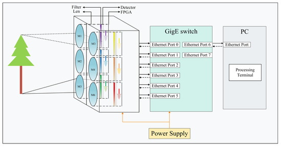
Figure 1.
Block diagram of the MSI system.
The system workflow is as follows: the pre-written camera control program is programmed into the FPGA’s flash chip. After the system powers on, the host PC sends unified parameter settings to the six camera nodes. When the conditions for the selected trigger mode are met, all nodes execute synchronous exposure and acquisition sequences. At the front end, each node’s FPGA performs lightweight preprocessing on the raw pixel stream, including valid pixel extraction, data buffering, and protocol encapsulation. The encapsulated data packets are sent to the switch via each node’s independent GigE port; the switch performs Layer-2 forwarding to aggregate and deliver the data streams at high speed to the host computer. At the host end, the main control software performs real-time identification, sorting, and channel mapping of the data packets based on pre-set channel IP and MAC addresses, and finally performs the reconstruction, display, and data storage of the multi-channel images.
2.2. Optical Design
2.2.1. Sensor
The choice of sensor is crucial in the design of a multispectral camera, directly dictating the imaging performance, overall system volume, and implementation complexity. Considering the demands for high resolution, broad spectral response, and cost-effectiveness across diverse application scenarios, this system employs the Sony IMX178 (Sony, Tokyo, Japan), which has the advantages of high resolution, high dynamic range, low readout noise, and a wide spectral range [34]. Its relative quantum efficiency curve is illustrated in Figure 2, which shows a spectral response across the 400–1000 nm wavelength range, reaching a peak around 520–530 nm and gradually decreasing at longer wavelengths. The sensor features an effective resolution of 3072 × 2048 pixels, a pixel size of 2.4 μm × 2.4 μm, an optical format of 1/1.8 inch, and utilizes a rolling-shutter mechanism. Its key technical parameters are summarized in Table 2.
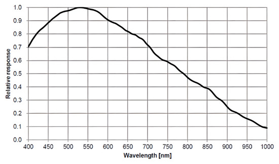
Figure 2.
Relative quantum efficiency of IMX178.

Table 2.
Main technical parameters of IMX178.
2.2.2. Filters
Narrowband interference filters are the key optical elements enabling band separation in the proposed MSI system. To ensure spectral flexibility, each camera node accepts independently interchangeable filters. As detailed in Table 3, the prototype utilizes six filters with specific center wavelengths and full-width-at-half-maximum (FWHM) bandwidths covering the visible to near-infrared spectrum. Compared with integrated MSFAs, this approach not only offers complete freedom in spectral configuration but also leverages mature and cost-effective commercial filter products, further reducing overall system cost.

Table 3.
Spectral configuration of narrowband filters for each channel.
2.2.3. Optical Lens
The selection of the optical lens directly influences the imaging performance of the system, particularly key parameters such as the Field of View (FOV), spatial resolution, and working distance. To maximize adaptability across diverse operational scenarios, this system employs lenses with the standard C-mount interface, as illustrated in Figure 3a. This widely adopted industrial standard offers excellent versatility and mechanical stability, along with access to a rich selection of commercially available lenses, facilitating flexible switching between laboratory testing and field deployment.
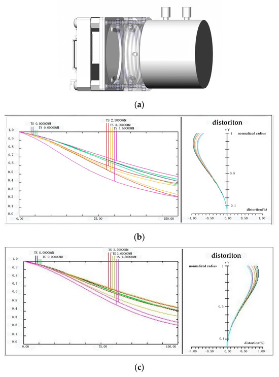
Figure 3.
(a) Schematic diagram of the C-mount lens interface design; (b) MTF chart for 8 mm C-mount lens, the colored curves plots represent different field heights TS from the image center to the rim; (c) MTF chart for 16 mm C-mount lens, the colored curves plots represent different field heights TS from the image center to the rim.
To ensure imaging quality, avoid vignetting or resolution loss caused by image-circle mismatch, and match the 1/1.8-inch optical format of the IMX178, two C-mount fixed-focal-length lenses (VM0820MP5 and VM1620MP5) from ZLKC (Guangzhou Zhisai Electronic Technology Co., Ltd., Guangzhou, China) were selected for the prototype: an 8 mm lens [35] and a 16 mm lens [36]. Their optical performances are shown in Figure 3b,c. For the 8 mm lens, the Modulation Transfer Function (MTF) curves are given at field heights TS = 0, 1.0, 2.5, 3.0 and 4.5 mm, i.e., from the image center to the rim of the 1/1.8″ format; at F2.0 the on-axis MTF stays close to 1.0 up to about 50 lp/mm and remains above roughly 0.35–0.4 at 100 lp/mm even at TS ≈ 4.5 mm. For the 16 mm lens, the MTF is plotted at TS = 0, 1.0, 2.8, 3.0 and 4.5 mm, likewise covering the whole usable image circle; its off-axis curves fall more slowly than those of the 8 mm lens and stay around 0.4 at 100 lp/mm at TS ≈ 4.5 mm, indicating that the longer-focal-length lens can better preserve fine detail of the 2.4-µm-pixel sensor. In practice, the 8 mm lens is used for wide-FOV, low-magnification or overview imaging, whereas the 16 mm lens is used for local, higher-resolution observation. Both lenses support manual focus and manual iris control, and have a maximum aperture of F2.0. In addition, the right-hand panels of Figure 3b,c show the corresponding distortion characteristics: the horizontal axis represents distortion in percent, and the vertical axis denotes the normalized exit-pupil radius, whose maximum value is 1. In both cases, the curves remain confined within ±0.1% over the full pupil. Detailed optical parameters for these lenses are presented in Table 4.

Table 4.
Main technical parameters of the selected C-mount lenses.
From an optical-design perspective, these choices form a compact multi-aperture front end that is explicitly matched to the 1/1.8″ image format of the sensors. The 8 mm and 16 mm C-mount lenses provide two representative working modes—one favoring a wider field of view and one favoring finer ground sampling—while their image circles fully cover the active sensor area to avoid vignetting and edge-resolution loss caused by image-circle mismatch. Together with the dedicated C-mount interface and filter holders, the lenses and narrowband interference filters can be exchanged without disturbing the relative alignment between the six camera nodes. This modular optical layout underpins the high spatial resolution and reconfigurable spectral configuration demonstrated by the proposed system.
2.2.4. Mechanical Structure Design
The system employs a unibody aluminum alloy housing, with its layout shown in Figure 4: the front section is dedicated to mounting optical components and sensing assemblies, while the rear section houses electronic elements. The front panel is designed as the optical datum of the system, featuring a precision-machined 2 × 3 array of six coaxial ports, each configured as a standard C-mount interface, with the detailed structure illustrated in Figure 3a. Behind each port, the narrowband filters are mounted via standard threaded interfaces directly in front of the sensor, which keeps the structure compact and enables quick filter replacement. The IMX178 carrier board and the FPGA-based sensor control board are mounted to the internal frame by means of hex standoffs and screws. To meet the stringent requirements for optical axis co-axiality, surface flatness, and shading margin at the front end, both the front panel and the lens barrel mounting plate are connected to the housing’s locating surfaces via countersunk screws.
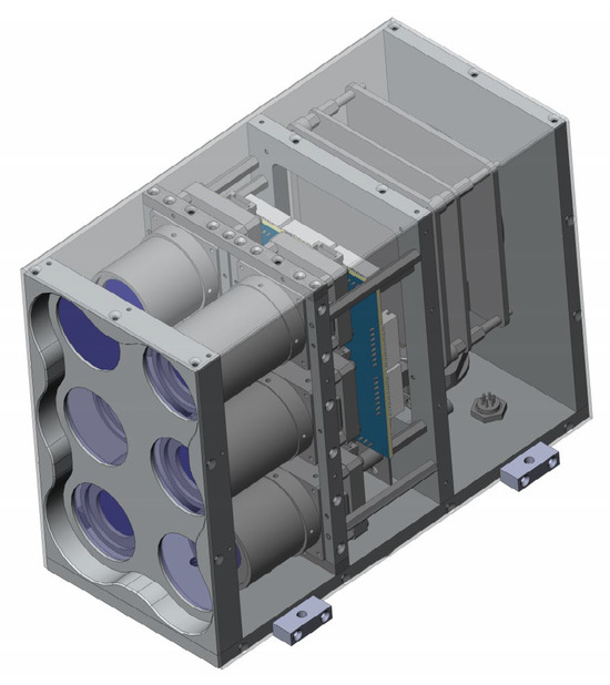
Figure 4.
Hardware structure design of the 2 × 3 multispectral camera array.
The mid-rear section of the housing forms the electronics mounting and support area. This section utilizes multiple sets of hex standoffs and screws to assemble internal partitions, upper support members, and the rear mounting surface into a rigid, lightweight space-frame structure according to predefined heights and spacing. This design establishes dimensionally controlled and repeatable mounting references for the switch, interface board, and power module. Simultaneously, it maintains continuous cable-routing paths and thermal-dissipation channels between the optical and electronic zones, facilitating subsequent debugging, module replacement, and system expansion. The overall design ensures the positional accuracy of the six-channel optical axes while balancing the accessibility for assembling electronic modules, ease of maintenance, and stiffness requirements for engineering integration. Overall, the combination of the mechanically registered housing, the IMX178 sensor modules, and the interchangeable lens–filter units results in a compact multi-aperture optical front end that maintains stable inter-channel alignment while allowing the spectral bands and focal lengths to be reconfigured for different applications.
2.3. FPGA-Based Control System
2.3.1. FPGA Specification
The selection of the FPGA requires a comprehensive evaluation of logic resources, memory capacity, I/O performance, power consumption, and cost to meet the system’s demands for high-resolution image processing and high-speed data transmission. Based on these considerations, the Xilinx Artix-7 FPGA (XC7A100T-CSG324, Xilinx Inc., San Jose, CA, USA) was chosen for this system. Its key features are outlined below:
- Sufficient Logic Resources: The XC7A100T provides approximately 101 K logic cells and 63 K LUTs, which are adequate to implement the critical logic for driving the IMX178 sensor, image preprocessing pipelines, data buffer control, and the GigE MAC, ensuring a solid hardware foundation for complex data-processing workflows.
- On-Chip Memory for Line Buffering: The integrated 4860 Kbits of Block RAM is crucial for handling high-resolution image data streams, effectively buffering multiple image lines to support real-time processing pipelines and prevent data loss due to rate mismatches.
- Compact Package: The CSG324 package offers a small footprint, making it highly suitable for the space-constrained design of the camera nodes and contributing to the overall miniaturization goals of the system.
- Rich I/O Resources: With 210 user I/O pins, this package provides sufficient connectivity to simultaneously support parallel interfaces to high-speed peripherals, meeting the design requirements for high-bandwidth, low-latency data paths.
This section details the internal FPGA-based control architecture designed for each camera node, as shown in Figure 5. The architecture consists of four functional subsystems: (i) a sensor control module that drives the IMX178, executes SPI-based register configuration, and reports sensor readback data; (ii) a device register map and arbitration module that provides a unified register space, mediates accesses from the network side, and forwards detector-related writes to the sensor control module; (iii) an image reception and buffering module that acquires LVDS image data, performs image processing, and stores the data in onboard image memory; and (iv) a GigE Vision communication module composed of an Ethernet RX/TX path and a GigE Vision Control Protocol (GVCP)/GigE Vision Streaming Protocol (GVSP) device engine, which decodes GVCP commands from the host, generates GVCP acknowledgements, and packetizes buffered image data into Ethernet frames for transmission through the RJ45 interface.
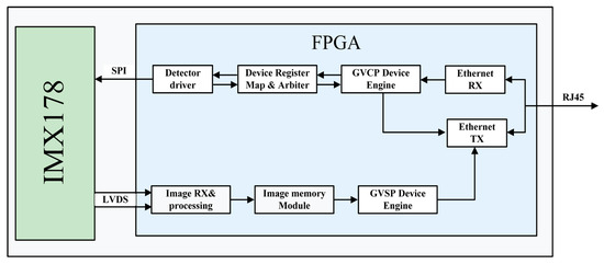
Figure 5.
FPGA-based architecture for IMX178 imaging and control.
2.3.2. Sensor Driver
The IMX178 requires a strict initialization process, as shown in Figure 6. First, the I/O pin settings and logic-level standards are established. This is followed by the power-on sequence, a system reset, and the reference clock input. Once these are configured, the process enters the unified “Register settings” phase. This step involves writing all necessary configuration parameters via serial communication, which includes both the initial values that must be changed as specified by the datasheet and other user-defined operational parameters. After all registers are written, the “standby cancel” command is executed, followed by a wait period for the internal regulator to stabilize (>16 ms). Once stable, the sensor determines its operating mode according to the external I/O: if master mode is selected, the IMX178 itself generates the frame-sync XVS and line-sync XHS signals; otherwise, the system operates in slave mode, receiving external XVS and XHS signals. The sensor then enters the “operation” state to begin exposure and data acquisition.
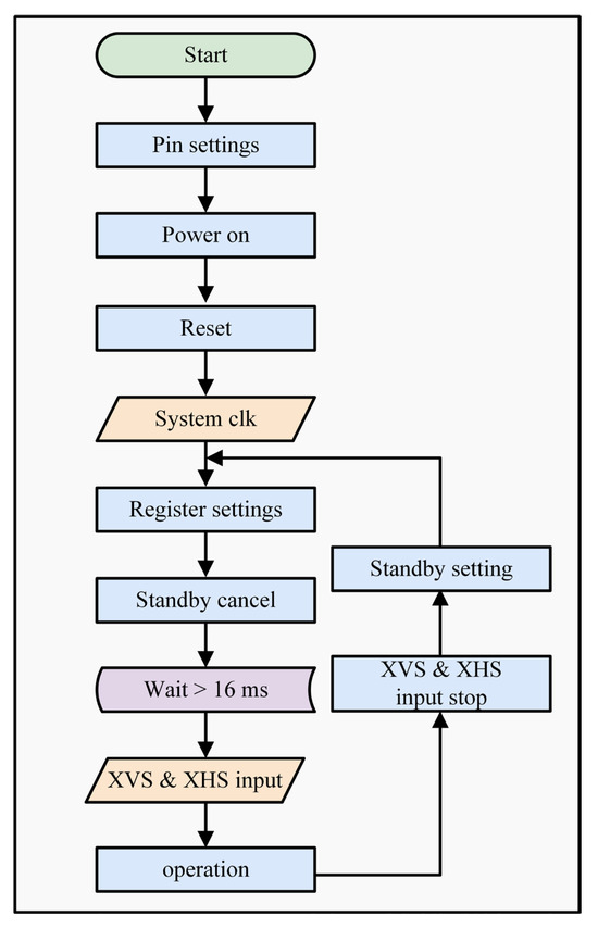
Figure 6.
IMX178 slave mode initialization flowchart.
The IMX178 latches its control-interface mode on the first access: if the device observes 4-wire serial timing with XCE pulled low, it enters the SPI mode; if XCE is held high and I2C timing is applied, it operates in I2C mode. In this work, the SPI mode is used. XCE is first driven low to enable the serial port. The serial clock (SCK) frequency is set to 8 MHz, which is below the 13.5 MHz limit specified in the datasheet. Data are transmitted LSB-first. Serial input data (SDI) are updated on the falling edge of SCK and latched on the rising edge. Registers are written in a continuous sequence: chip ID → start address → consecutive data bytes. After configuration, the serial output data (SDO) line is used to read back registers; the FPGA Sensor Control Module compares the returned values and, if mismatched, rewrites the corresponding entries to ensure that the sensor enters the intended mode. In the prototype, the IMX178 is driven by a 27 MHz reference and runs in the full-frame 6.3 M all-pixel scan (3072 × 2048) mode with the 8-channel LVDS output enabled.
2.3.3. Device Register Map and Arbitration
The device register map and arbitration block form a single address space for the whole node. All GVCP read and write commands from the host are applied to this address space first. The register space is split into two parts. The first part consists of system registers. These hold items such as the local IP, MAC address, and GVSP destination. A write from the PC to this part is stored immediately, and a read is returned immediately. The second part is sensor registers. These describe IMX178 settings that must be written through SPI. When the PC writes to such an address, the arbiter stores the value, starts an SPI write through the Sensor Control Module, and marks this register as pending. After the sensor is read back through SDO and the same value is confirmed, the arbiter clears the pending mark and overwrites the register with the confirmed value. A later GVCP read to this address will return the confirmed value from the sensor. In this way, the PC always sees one consistent register map.
2.3.4. FPGA-Based Data Processing and Storage
The module adopts a three-stage pipeline: (i) LVDS reception and deserialization, (ii) image alignment, and (iii) frame buffering. After standby cancelation, the FPGA waits for the on-chip regulator to stabilize and discards the first eight warm-up frames. Valid images are output from the ninth frame onward.
The sensor outputs LVDS DDR data, which the FPGA samples on both edges of the LVDS clock. The system uses the line-level sync codes as anchors. It establishes a stable word boundary using a bit-slip operation and performs deskew operations to eliminate phase differences between lanes. If sync codes are lost or word boundaries drift, the deserialization state machine automatically reverts to a training state to re-acquire lock. Subsequently, based on the sync codes and line/frame counters, the logic strips away the non-pixel data components, such as the horizontal blanking and vertical blanking intervals, which is achieved via BRAM-based address mapping. To facilitate subsequent processing and buffering, the valid pixels are first left-aligned and extended to a uniform 16-bit format. The data then pass through a FIFO that simultaneously performs clock-domain crossing and data-width conversion, after which the organized row-based pixel stream is forwarded to the DDR3 storage module.
The system utilizes an AXI-based DMA IP core, the Memory Interface Generator (MIG) core, and a ping-pong frame buffering mechanism to decouple pixel data storage. While the pixel stream is written to Buffer A via the AXI bus, the full Buffer B is read out for transmission; their roles are swapped at the frame boundary. This ping-pong architecture avoids complex bus arbitration and multi-level buffering. The DMA IP’s address width and data width are configured to match the parameters of the MIG S_AXI interface.
At the control-logic level, both the DMA’s write (Stream to Memory-Mapped, S2MM) and read (Memory-Mapped to Stream MM2S) operations use a single line as the basic transport unit. The frame-processing logic provides the base address of the current frame and the line length in bytes. For example, with the IMX178 operating at 3072 pixels per line and 16-bit pixels (i.e., 6144 bytes per line), the DMA runs on a 200 MHz AXI clock, the M_AXI data bus is 64 bits wide, and the maximum burst length is set to 256 beats, as shown in Figure 7. Under this configuration, one line is automatically split into three full AXI write bursts; the DMA asserts WLAST on the final beat of each burst and increments the AXI address until all 6144 bytes have been written. The MM2S read path follows the same rule. Therefore, the upper-level application logic can achieve stable, reliable line-level data transport without managing low-level details such as DDR3 physical alignment, burst boundaries, or address stepping.
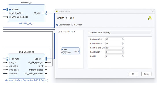
Figure 7.
Line-based DMA configuration and connection to the DDR3 buffer.
2.3.5. Image Output Control
To meet the requirements of high throughput, low latency, and deterministic logic, this system uses the GigE Vision protocol for image data stream transmission. During power on, the control path reads the GVSP-related configuration from the register map and arbitration module and returns it to the host through GVCP so that the host always knows the current sensor and network configuration stored inside the FPGA. The image channel is simplified and only carries pixel data together with the frame identifier (Block ID) and the packet identifier (Packet ID). Static information, such as image size, pixel format, or destination port, is not repeated in every GVSP packet, which increases the useful payload ratio. When the host later issues GVCP commands that modify sensor registers, the register map forwards those writes and data to the Sensor Control Module. Figure 8a shows the GVCP traffic captured during operation. The host periodically issues GVCP read commands to the register map, and the FPGA responds with read ACK messages whose payload is 0xC0A8000A. This confirms that the control plane can correctly access the unified register map inside the FPGA.
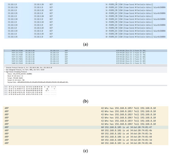
Figure 8.
(a) GVCP data stream capture; (b) GVCP control stream capture; (c) ARP exchanges between the host and camera nodes capture.
For each image frame, the FPGA generates a monotonically increasing Block ID, and for every UDP packet belonging to that frame, it assigns a consecutive Packet ID. With this two-level index, the host can perform reordering, loss detection, and complete frame reconstruction even when packets arrive out of order. As illustrated in Figure 8b, Wireshark traces from two camera nodes show standard Ethernet/IPv4/UDP headers followed by a GVSP header and pure image payload, with both nodes using the same Block ID for the same frame while maintaining independent Packet ID sequences. The static imaging parameters had already been configured through GVCP, so they were not repeated in the GVSP payload.
2.4. System Control and Synchronization
2.4.1. Multi-Camera Data Exchange and Communication Interfaces
To enable management and data aggregation of the 2 × 3 multi-camera nodes, the system adopts a unified address plan and layered communication strategy on the Ethernet side. All FPGA imaging nodes are placed in the same subnet and assigned unique MAC and IP addresses, as summarized in Table 5. On the control plane, the host uses UDP port 3956 for GVCP to access each node by IP for register read/write, runtime parameter configuration, and acquisition control. On the data plane, each node binds its GVSP image stream to a dedicated Ethernet port, so different cameras can be distinguished simply by the “source MAC + source IP” tuple. Initial contact follows the standard ARP procedure. Subsequent GVCP and GVSP traffic is sent as unicast, consistent with the ARP exchanges shown in Figure 8c.

Table 5.
Network address assignment for multi-camera nodes.
All camera nodes and the host are connected to a GigE switch in a star topology. The switch operates as a Layer-2 learning bridge and forwards frames based on destination MAC addresses without modifying IP, UDP, or GVSP fields. Since each FPGA node outputs complete GVSP packets, the Block ID and Packet ID generated at the source arrive at the host unchanged, ensuring accurate frame reconstruction and loss detection. The main technical parameters of the selected switch are listed in Table 6. The current system is designed for a theoretical uplink capacity of 1 Gb/s; when all six camera nodes transmit GVSP image streams simultaneously, the switch buffers and arbitrates packets from the six ingress ports and forwards them toward the host at the uplink rate.

Table 6.
Main technical parameters of the GigE switch.
2.4.2. Power Management and Trigger Implementation
The system uses an external 28 VDC source as the common input and first converts it to a regulated 12 VDC bus through a high-efficiency DC–DC module. This bus supplies both the onboard GigE switch and the camera nodes. On each camera node, the 12 V rail is further stepped down by onboard LDOs to generate the required low-voltage rails. The key electrical specifications of the front-end 28 V to 12 V DC–DC module are summarized in Table 7. This hierarchical supply scheme, which combines a centralized 28 V bus step-down with node-level multi-rail regulation, centralizes the high-voltage conversion at the front end, reducing the thermal and space burden on each camera board and ensuring that all nodes start up from a common voltage reference, thereby providing a stable and consistent power basis for external trigger distribution and multi-camera synchronization.

Table 7.
Main technical parameters of the DC–DC buck converter module.
The system supports two operating modes: internal triggering and external triggering. In internal mode, each camera runs independently, but the shared 1 GbE uplink may cause image tearing, frame loss, longer stabilization period, and unbalanced channel bandwidth. The external trigger mode is divided into software and hardware triggers. The software trigger relies on the host PC broadcasting GVCP acquisition commands to all six nodes, but this method is unreliable for high-precision synchronization due to significant timing jitter introduced by Ethernet transport and switch queuing. To obtain deterministic timing, the system adopts a unified hardware trigger driven from an FPGA GPIO pin, whose circuit is shown in Figure 9a. When Line 0 is pulled low, the diode conducts and pulls the GPI low; when Line 0 is driven high by the external supply, the diode blocks the high voltage, and the GPI returns to its pull-up level, forming a rising-edge trigger. The electrical characteristics of this GPIO, as detailed in Table 8, include a rise time of less than 1 μs, and the input high level is specified as 1.5–30 VDC. Therefore, the camera nodes directly use the system’s 28 VDC power supply as the source of the Line 0 level, and the trigger line is controlled by a toggle switch to simplify operation.
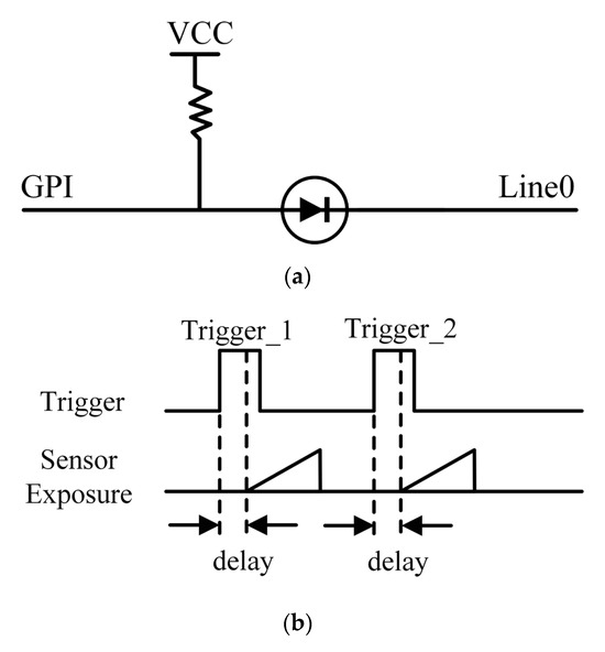
Figure 9.
(a) GPIO-based hardware trigger input circuitry; (b) timing diagram of the trigger with configurable delay.

Table 8.
Electrical properties of the GPIO pin for hardware triggering.
In external trigger mode, the system supports configurable trigger delays. As illustrated by the timing diagram in Figure 9b, upon detecting the trigger’s rising edge, the camera waits for a user-defined delay period before initiating exposure. This design offers two key advantages: first, it decouples the physical trigger edge from the actual exposure, filtering out pulse jitter and glitches; second, it allows identical delays to be loaded across all cameras to compensate for internal processing differences, ensuring highly consistent and synchronous exposure across the entire array.
2.5. Host-Side Software Architecture and Implementation
To interoperate with the FPGA-based image acquisition and GVSP streaming mechanism on the front end, an MFC-based multi-channel host application is implemented on the PC side, providing unified camera access, parameter configuration, real-time visualization, and image archiving. As shown in Figure 10, this software architecture is divided into three layers: the MFC GUI layer, the Device management layer, and the GigE Vision SDK layer. The MFC GUI utilizes a dialog-based design, integrating six display panes and all acquisition controls into a single window for centralized supervision of the camera array. To prevent UI blocking, while the GUI thread is restricted to event handling, data reception, frame reconstruction, and disk operations are executed in background worker threads.
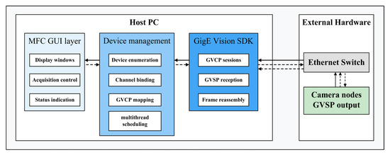
Figure 10.
Multi-channel GigE Vision software (version 1.0, UCAS, Beijing, China) system architecture.
The communication layer is built on top of a GigE Vision-compliant SDK. This SDK asynchronously performs three core tasks: (i) establishing GVCP control sessions for register read/write operations and configuration; (ii) receiving and reconstructing GVSP image streams according to the protocol; and (iii) exposing the reassembled frames to the application. Because the SDK hides complexities such as packet encapsulation, port management, and retransmission, the MFC layer only needs to interact with a “device instance + image frame” abstraction, which significantly reduces implementation complexity.
Based on this communication layer, application-level functions consistent with the system workflow are implemented. At startup, the program invokes the SDK’s enumeration API to discover all reachable imaging nodes on the Ethernet and binds them, in order, to the six pre-allocated display channels, following a “discover-and-bind” policy. When the user adjusts exposure, switches the trigger mode, or starts/stops acquisition on a given channel, the operation is translated into a GVCP command to the target device.
For image reception and visualization, each active channel spawns a dedicated acquisition and display thread. This thread pulls already reassembled frames from the SDK and delivers them to the corresponding MFC control via a fixed ID mapping, achieving synchronous visualization of multiple streams. Image storage runs in parallel with display. The application generates a filename for each new frame, incorporating its channel ID, resolution, and frame index before writing it to disk. Furthermore, a mutex is employed to prevent write collisions when multiple channels save data simultaneously, ensuring reliable storage in multi-camera scenarios.
The software architecture detailed in Figure 10 is implemented as the host application’s main interface, shown in Figure 11. This interface, built as an MFC dialog, integrates all monitoring functions for the 2 × 3 camera array into a single window to achieve centralized supervision. The main body consists of six independent display panes, one for each node from Cam1 to Cam6, which provide visualization and display statistics. The control panel on the right provides direct access to core functions. Users can switch between nodes via camera select and independently adjust exposure control, gain control, and pixel format. These operations are ultimately translated by the Device management layer into GVCP access commands for the target node. Finally, the status bar at the bottom provides feedback on device enumeration and operational status.

Figure 11.
Host application main interface.
2.6. Integrated Hardware Architecture Design
Figure 12a shows the physical prototype of the 2 × 3 multispectral camera array, and Figure 12b illustrates its internal layout. The hardware architecture is essentially consistent with that in Figure 4: within a compact enclosure, it integrates six camera nodes, a GigE switch, and a DC–DC power module. The unit is powered through a single 28 VDC input and uses one GigE port for both data and control.
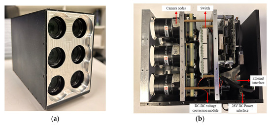
Figure 12.
(a) Assembly diagram of the 2 × 3 multispectral camera array; (b) Internal structure diagram of the 2 × 3 multispectral camera array.
The system adopts an integrated, lightweight design with overall dimensions of 156 × 74 × 118 mm and a total mass of about 1.26 kg. Measurements under a 28 VDC supply indicate a stable operating power of 24.08–24.92 W. To meet deployment requirements in harsher environments, all key components are selected in industrial versions and, together with the enclosure’s thermal design, the recommended operating ambient temperature can be set to approximately −10 °C to 60 °C to ensure reliable long-term operation, which is summarized in Table 9.

Table 9.
System-level mechanical and electrical parameters of the integrated system.
3. Results
3.1. Performance Validation of the MSI System
To verify end-to-end functionality and synchronization, the camera array was operated in hardware-triggered mode with a pixel bit depth of 12 bits. In this paper, a combined theoretical analysis and prototype-based experimental evaluation scheme [37] is employed to assess the performance of the MSI system. We equipped lenses with focal lengths of 8 mm and 16 mm, and tested two sets of narrowband filters with different center wavelengths under both lens configurations. The host computer’s acquisition interface synchronously displayed the real-time images of the six channels (M1–M6) and recorded the operating status. Frame-counting monitoring showed no frame or packet loss, indicating that the six data streams were acquired stably and synchronously under unified triggering. Figure 13a and 13b are screenshots of the acquisition under the 8 mm and 16 mm configurations, respectively: the 8 mm configuration achieves wider scene coverage, while the 16 mm configuration presents finer spatial details. To ensure a consistent field of view across the six channels and to facilitate subsequent registration, window cropping was enabled in each channel to select identical and center-aligned overlapping areas. The effective spatial resolution at the two focal lengths is approximately 3.6 MP (8 mm) and 4.7 MP (16 mm), respectively, further verifying the system’s synchronous acquisition capability and imaging stability at different focal lengths.
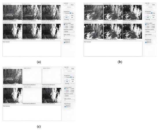
Figure 13.
(a) Image acquisition using an 8 mm focal length lens and filter configuration 1; (b) Image acquisition using a 16 mm focal length lens and filter configuration 2; (c) Three-channel image acquisition using a 16 mm lens and filter configuration 2. In all subfigures, the spectral bands are labeled as BAND1–BAND6, where BAND1–BAND6 denote the first to sixth spectral channels, and the corresponding center wavelengths are listed in Table 3.
In addition, the system supports the acquisition of multispectral images from any of the six channels, as shown in Figure 13b,c. Calculations indicate that when operating with a single camera, the system achieves a frame rate of approximately 18 fps at a resolution of 3072 × 2048 and 12-bit depth, corresponding to an effective data throughput of about 880 Mb/s, approaching the transmission limit of a GigE port. Even with six camera nodes operating concurrently, the system reliably completes the acquisition, display, and storage of full-resolution images, as detailed in Table 10. Compared with the representative domestically developed multi-aperture MSI cameras summarized in Table 1, the proposed system achieves a higher effective spatial resolution and, more importantly, a reconfigurable lens and filter configuration that can be adapted to different tasks and spectral band selections.

Table 10.
Key specifications and performance benchmarks of the proposed reconfigurable MSI system.
3.2. Data Processing
To evaluate the spectral performance of the multispectral camera array, we generated an RGB composite from the 16 mm dataset by mapping three selected bands to the R, G, and B channels, as shown in Figure 14a,b. To compare the spectral characteristics of different land features, we selected different locations for spectral curve extraction. In Figure 14a, the selected region corresponds to vegetation, and its spectral profile on the right shows a characteristic pattern with relatively high values in specific bands, reflecting the typical spectral response of green plants. In contrast, Figure 14b focuses on a region representing road surfaces, and its spectral profile exhibits distinctly different trends, with lower values in most bands compared to vegetation. These contrasts demonstrate that the system captures discriminative band-dependent signatures and provides good spectral response characteristics.
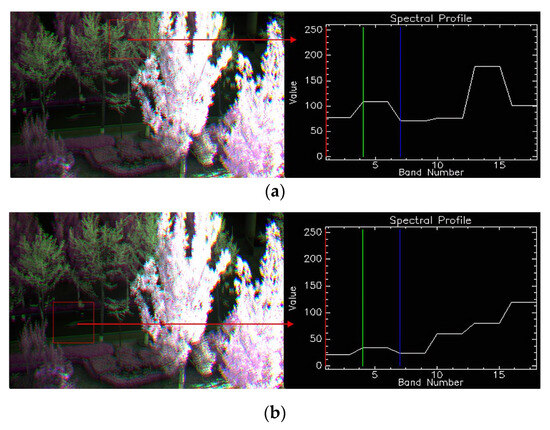
Figure 14.
(a) Vegetation ROI—RGB composite and spectral profile using the 16 mm focal length lens; (b) Road-surface ROI—RGB composite and spectral profile using the 16 mm focal length lens.
4. Discussion
Focusing on spectral flexibility, portability, and high resolution, this study presents a 2 × 3 multispectral camera array that allows for the flexible replacement of lenses and filters. The front-end imaging design adopts a distributed architecture, in which an FPGA at each imaging node performs independent sensor control and data pre-processing. The high degree of parallelism and low latency are ideal for processing high-speed data streams from high-resolution sensors. Regarding array synchronization, the FPGA’s ability to respond directly to external trigger signals at the hardware level enables microsecond-level timing control, which is critical for eliminating inter-channel timing jitter and for offloading real-time tasks such as GigE packetizing from the host computer.
The MFC-based master control software, built on the GigE Vision protocol, achieves synchronized acquisition, real-time display, and unified parameter configuration for all six channels. It also supports flexible control of any single camera or multiple camera combinations. The system supports both internal and external trigger modes. Internal triggering is suitable for standalone operation of a single camera node, whereas the external trigger mode, especially the hardware-trigger solution, provides programmable trigger-delay capabilities, effectively eliminating timing jitter and providing reliable assurance for high-precision synchronized acquisition across multiple cameras.
End-to-end performance verification has confirmed that the system possesses stable, high-resolution, and highly flexible synchronous acquisition capabilities. The system exhibits discriminative band-dependent signatures for different land features, demonstrating good spectral response characteristics. In this work, the experimental evaluation primarily focuses on frame rate and end-to-end throughput under multi-camera acquisition. A limitation of the experiment is that a detailed quantitative characterization of the latency during multi-channel operation has not yet been performed. Due to the current development status, this in-depth latency profiling is left for future work.
At the same time, the present prototype mainly aims to validate the reconfigurable hardware architecture and acquisition pipeline, so the experiments are still performed on raw sensor digital numbers without a complete radiometric, spectral, and geometric calibration workflow [38]. From a radiometric perspective, only basic preprocessing is applied; we have not yet carried out systematic dark-frame and flat-field acquisition, vignetting compensation, or band-wise radiometric calibration with reference targets, so the reported results should be interpreted as qualitative rather than fully calibrated reflectance. In the spectral domain, we currently rely on the nominal center wavelengths and FWHM specified for the interference filters and treat each channel as an ideal narrowband bandpass; a more rigorous spectral calibration will require measuring the end-to-end spectral response of each channel, deriving effective band centers and bandwidths, and incorporating these response curves into subsequent spectral analysis [39]. Spatially, approximate co-registration is achieved by applying identical window cropping on all six sensors so that the fields of view largely overlap, but residual mechanical and optical tolerances still introduce inter-band shifts of about 2–4 pixels. Future versions of the system will therefore integrate a dedicated cross-channel registration [15] module based on calibration targets and sub-pixel geometric correction to enable pixel-accurate multispectral analysis.
5. Conclusions
A reconfigurable 2 × 3 multispectral camera-array imaging system developed in this study achieves stable, high-resolution, synchronized acquisition while maintaining a compact size. The system supports internal and external hardware triggers, real-time display and storage, and flexible per-node or grouped control. This modular design, combined with a robust high-throughput data link, provides a high-resolution and flexibly deployable solution for real-time, portable MSI that can meet the needs of diverse application scenarios.
In future work, we plan to conduct field tests with the system to further validate its performance in real-world scenarios. In parallel, we will refine the calibration and back-end image processing pipeline, including radiometric and spectral calibration, automated cross-channel image co-registration, and real-time spectral analysis algorithms.
Author Contributions
Conceptualization, M.H. and L.Q.; methodology, Z.W.; software, Z.W., X.L., G.W., Y.Z. and S.C.; validation, Z.W., G.W. and S.C.; formal analysis, G.W. and Y.Z.; investigation, Z.W. and S.C.; resources, L.Q., W.G. and J.C.; data curation, Z.W. and S.C.; writing—original draft preparation, S.C.; writing—review and editing, Z.W.; visualization, S.C., W.G. and J.C.; supervision, M.H.; project administration, L.Q.; funding acquisition, M.H. All authors have read and agreed to the published version of the manuscript.
Funding
This research was funded by the “Future Star” talent program of the Aerospace Information Research Institute, Chinese Academy of Sciences, and the Youth Innovation Promotion Association, CAS.
Institutional Review Board Statement
Not applicable.
Informed Consent Statement
Not applicable.
Data Availability Statement
The original contributions presented in this study are included in the article. Further inquiries can be directed to the corresponding author.
Conflicts of Interest
Author Wenbin Ge was employed by Aviation Industry Corporation of China Guizhou Aircraft Co., Ltd. The remaining authors declare that the research was conducted in the absence of any commercial or financial relationships that could be construed as a potential conflict of interest.
Abbreviations
The following abbreviations are used in this manuscript:
| MSI | Multispectral imaging |
| GigE | Gigabit Ethernet |
| MFC | Microsoft Foundation Class |
| SDK | Software Development Kit |
| FPGA | Field Programmable Gate Array |
| FWHM | Full Width at Half Maximum |
| MSFAs | Multi-Spectral Filter Arrays |
| FOV | Field of View |
| MTF | Modulation Transfer Function |
| GVCP | GigE Vision Control Protocol |
| GVSP | GigE Vision Streaming Protocol |
| SCK | Serial clock |
| SDI | Serial input data |
| SDO | Serial output data |
| MIG | Memory Interface Generator |
| S2MM | Stream to Memory-Mapped |
| MM2S | Memory-Mapped to Stream |
References
- Shen, F.; Deng, H.; Yu, L.; Cai, F. Open-Source Mobile Multispectral Imaging System and Its Applications in Biological Sample Sensing. Spectrochim. Acta A Mol. Biomol. Spectrosc. 2022, 280, 121504. [Google Scholar] [CrossRef] [PubMed]
- Mukhtar, S.; Arbabi, A.; Viegas, J. Compact Spectral Imaging: A Review of Miniaturized and Integrated Systems. Laser Photonics Rev. 2025, 19, e01042. [Google Scholar] [CrossRef]
- Khodabakhshian, R.; Emadi, B.; Khojastehpour, M.; Golzarian, M.R. Determining quality and maturity of pomegranates using multispectral imaging. J. Saudi Soc. Agric. Sci. 2017, 16, 322–331. [Google Scholar] [CrossRef]
- Cardim Ferreira Lima, M.; Krus, A.; Valero, C.; Barrientos, A.; del Cerro, J.; Roldán-Gómez, J.J. Monitoring Plant Status and Fertilization Strategy through Multispectral Images. Sensors 2020, 20, 435. [Google Scholar] [CrossRef]
- Liu, S.; Zhang, J.; Ma, Y. Bathymetric ability of SPOT-5 multi-spectral image in shallow coastal water. In Proceedings of the 18th International Conference on Geoinformatics, Beijing, China, 18–20 June 2010. [Google Scholar]
- Pour, A.B.; Zoheir, B.; Pradhan, B.; Hashim, M. Editorial for the Special Issue: Multispectral and Hyperspectral Remote Sensing Data for Mineral Exploration and Environmental Monitoring of Mined Areas. Remote Sens. 2021, 13, 519. [Google Scholar] [CrossRef]
- De Biasio, M.; Arnold, T.; Leitner, R. UAV-based multispectral imaging system for environmental monitoring. Tech. Mess. 2011, 78, 503–507. [Google Scholar] [CrossRef]
- Crihalmeanu, S.; Ross, A. Multispectral scleral patterns for ocular biometric recognition. Pattern Recognit. Lett. 2012, 33, 1860–1869. [Google Scholar] [CrossRef]
- Hassan-Esfahani, L.; Torres-Rua, A.; Ticlavilca, A.M.; Jensen, A.; McKee, M. Topsoil moisture estimation for precision agriculture using unmanned aerial vehicle multispectral imagery. In Proceedings of the 2014 IEEE Geoscience and Remote Sensing Symposium, Quebec City, QC, Canada, 13–18 July 2014. [Google Scholar]
- Bamane, K.D.; Kumaraguru, S.; Gohil, D.; Sinkar, Y.; Gaikwad, A.; Bhamare, D.S. Enhancement in Multi Spectral Camera System for Precision Agriculture using NDVI Calculation Algorithm. Front. Health Inform. 2024, 13, 4728–4741. [Google Scholar]
- Barjaktarovic, M.; Santoni, M.; Bruzzone, L. Design and verification of a low-cost multispectral camera for precision agriculture application. IEEE J. Sel. Top. Appl. Earth Obs. Remote Sens. 2024, 17, 6945–6957. [Google Scholar] [CrossRef]
- Zapata, F.; López-López, M.; Amigo, J.M.; García-Ruiz, C. Multi-spectral imaging for the estimation of shooting distances. Forensic Sci. Int. 2018, 282, 80–85. [Google Scholar] [CrossRef]
- Wilk, L.S.; Hoveling, R.J.M.; van Velthoven, M.F.A.M.; Nijs, H.G.T.; Aalders, M.C.G. Optimizing the detection and characterization of bruises using multispectral imaging. J. Forensic Leg. Med. 2025, 111, 102811. [Google Scholar] [CrossRef]
- Hashimoto, K.; Mizuno, H.; Nakagawa, K.; Horisaki, R.; Iwasaki, A.; Kannari, F.; Sakuma, I.; Goda, K. High-Speed Multispectral Videography with a Periscope Array in a Spectral Shaper. Opt. Lett. 2014, 39, 6942–6945. [Google Scholar] [CrossRef]
- Genser, N.; Seiler, J.; Kaup, A. Camera array for multi-spectral imaging. IEEE Trans. Image Process. 2020, 29, 9234–9249. [Google Scholar] [CrossRef]
- Li, L.; Zheng, X.; Zhao, K.; Li, X.; Meng, Z.; Su, C. Potential evaluation of high spatial resolution multi-spectral images based on unmanned aerial vehicle in accurate recognition of crop types. J. Indian Soc. Remote Sens. 2020, 48, 1471–1478. [Google Scholar] [CrossRef]
- Vila-Francés, J.; Calpe-Maravilla, J.; Gómez-Chova, L.; Amorós-López, J. Design of a Configurable Multispectral Imaging System Based on an AOTF. IEEE Trans. Ultrason. Ferroelectr. Freq. Control. 2011, 58, 259–262. [Google Scholar] [CrossRef] [PubMed]
- Tran, M.H.; Fei, B. Compact and ultracompact spectral imagers: Technology and applications in biomedical imaging. J. Biomed. Opt. 2023, 28, 040901. [Google Scholar] [CrossRef] [PubMed]
- König, K. Multimodal Multiphoton Tomography with a Compact Femtosecond Fiber Laser. J. Opt. Photonics Res. 2024, 1, 51–58. [Google Scholar] [CrossRef]
- Hagen, N.; Kudenov, M.W. Review of snapshot spectral imaging technologies. Opt. Eng. 2013, 52, 090901. [Google Scholar] [CrossRef]
- Mukhtar, S.; Arbabi, A.; Viegas, J. Advances in spectral imaging: A review of techniques and technologies. IEEE Access 2025, 13, 35848–35902. [Google Scholar] [CrossRef]
- Daffara, C.; Pampaloni, E.; Pezzati, L.; Barucci, M.; Fontana, R. Scanning multispectral IR reflectography (SMIRR): An advanced tool for art diagnostics. Acc. Chem. Res. 2010, 43, 847–856. [Google Scholar] [CrossRef]
- Chao, K.; Yang, C.C.; Kim, M.S. Spectral line-scan imaging system for high-speed non-destructive wholesomeness inspection of broilers. Trends Food Sci. Technol. 2010, 21, 129–137. [Google Scholar] [CrossRef]
- Brauers, J.; Schulte, N.; Aach, T. Multispectral filter-wheel cameras: Geometric distortion model and compensation algorithms. IEEE Trans. Image Process. 2008, 17, 2368–2380. [Google Scholar] [CrossRef] [PubMed]
- Vila-Francés, J.; Calpe-Maravilla, J.; Gómez-Chova, L.; Amorós-Lopez, J. Analysis of acousto-optic tunable filter performance for imaging applications. Opt. Eng. 2010, 49, 113203. [Google Scholar] [CrossRef]
- Bianco, G.; Bruno, F.; Muzzupappa, M. Multispectral data cube acquisition of aligned images for document analysis by means of a filter-wheel camera provided with focus control. J. Cult. Herit. 2013, 14, 190–200. [Google Scholar] [CrossRef]
- Song, H.; Mehdi, S.R.; Wu, C.; Li, Z.; Gong, H.; Ali, A.; Huang, H. Underwater spectral imaging system based on liquid crystal tunable filter. J. Mar. Sci. Eng. 2021, 9, 1206. [Google Scholar] [CrossRef]
- Lapray, P.-J.; Wang, X.; Thomas, J.-B.; Gouton, P. Multispectral Filter Arrays: Recent Advances and Practical Implementation. Sensors 2014, 14, 21626–21659. [Google Scholar] [CrossRef]
- Mohammadi, V.; Gouton, P.; Rossé, M.; Katakpe, K.K. Design and development of large-band Dual-MSFA sensor camera for precision agriculture. Sensors 2023, 24, 64. [Google Scholar] [CrossRef]
- Huang, F.; Chen, Y.; Wang, X.; Wang, S.; Wu, X. Spectral clustering super-resolution imaging based on multispectral camera array. IEEE Trans. Image Process. 2023, 32, 1257–1271. [Google Scholar] [CrossRef]
- Wagadarikar, A.; John, R.; Willett, R.; Brady, D. Single Disperser Design for Coded Aperture Snapshot Spectral Imaging. Appl. Opt. 2008, 47, B44–B51. [Google Scholar] [CrossRef]
- Gehm, M.E.; John, R.; Brady, D.J.; Willett, R.M.; Schulz, T.J. Single-Shot Compressive Spectral Imaging with a Dual-Disperser Architecture. Opt. Express 2007, 15, 14013–14027. [Google Scholar] [CrossRef]
- Li, X.; Hu, Y.; Jie, Y.; Zhao, C.; Zhang, Z. Dual-Frequency Lidar for Compressed Sensing 3D Imaging Based on All-Phase Fast Fourier Transform. J. Opt. Photonics Res. 2023, 1, 74–81. [Google Scholar] [CrossRef]
- Sony Semiconductor Solutions. Available online: https://www.sony-semicon.com/files/62/flyer_security/IMX178LQJ_Flyer.pdf (accessed on 3 November 2025).
- ZLKC LENS. Available online: https://www.zhi-sai.com/en/pro.php?id=421 (accessed on 3 November 2025).
- ZLKC LENS. Available online: https://www.zhi-sai.com/en/uploadfile/file/DS/VM1620MP5.pdf (accessed on 3 November 2025).
- Dhanush Devappa, B.C.; Pawar, K.; Jain, S.; Murthy, A.V.R. Performance Evaluation of Underwater Optical Communication System Using Numerical and Physical Modeling. J. Opt. Photonics Res. 2025. online first. [Google Scholar]
- Guo, Y.; Senthilnath, J.; Wu, W.; Zhang, X.; Zeng, Z.; Huang, H. Radiometric Calibration for Multispectral Camera of Different Imaging Conditions Mounted on a UAV Platform. Sustainability 2019, 11, 978. [Google Scholar] [CrossRef]
- López-Álvarez, M.; Hernández-Andrés, J.; Romero, J.; Campos, J.; Pons, A. Calibrating the Elements of a Multispectral Imaging System. J. Imaging Sci. Technol. 2009, 53, 031102. [Google Scholar] [CrossRef]
Disclaimer/Publisher’s Note: The statements, opinions and data contained in all publications are solely those of the individual author(s) and contributor(s) and not of MDPI and/or the editor(s). MDPI and/or the editor(s) disclaim responsibility for any injury to people or property resulting from any ideas, methods, instructions or products referred to in the content. |
© 2025 by the authors. Licensee MDPI, Basel, Switzerland. This article is an open access article distributed under the terms and conditions of the Creative Commons Attribution (CC BY) license (https://creativecommons.org/licenses/by/4.0/).