1. Introduction
As electronic warfare (EW) systems have gained significant attention in military applications, there have been increasing demands for receiving antennas that can be integrated into aircraft [
1,
2,
3]. To enable the detection of electromagnetic emissions from various wireless communication and radar systems, wideband array antennas with beamforming capabilities are required for EW systems [
4,
5]. Moreover, circularly polarized (CP) antennas are preferred to mitigate the polarization mismatch caused by multipath fading [
6,
7]. Thus, various studies have been conducted to implement wideband CP array antennas [
8,
9,
10]. In [
11,
12,
13], tapered slot array antennas were proposed. Using a dual-port excitation with 90° phase delay, the array antennas can achieve a wideband CP beamforming property. However, the antenna dimension along the propagation direction is too large, making them unsuitable for integration into aircraft platforms. Spiral array antennas, as proposed in [
14,
15], offer a wide impedance bandwidth and a low-profile design. Nevertheless, the physical size of the array element exceeds a half-wavelength at the highest operating frequency, leading to grating lobes in the high-frequency band. Recently, there has been research into connected arrays with wideband characteristics [
16,
17,
18]. In connected arrays, electric (or magnetic) dipoles are periodically arranged and series-connected. This configuration allows current to flow in a lateral direction with small reflection, thereby enabling wideband impedance matching. Unlike tapered slot antennas that require large physical dimensions along the propagation direction, connected arrays provide a low-profile structure [
19]. Furthermore, since the size of each array element is typically a half-wavelength at the highest operating frequency, the grating lobe issues can be minimized. To further enhance the performance of connected arrays, such as impedance matching, scanning angle [
20], and front/back ratio [
21], research has explored the use of artificial dielectric layers (ADLs) as superstrates. By manipulating the sub-wavelength metallic patterns printed on multi-layer dielectric substrates, the gap between the patches, and the inter-layer distance, the desired effective permittivity can be realized. Unlike electromagnetic bandgap structures, ADLs exhibit low dispersion properties, which is important in wideband antenna operation. In [
22], 4 × 4 array antennas were proposed for wideband CP beamforming. Despite the successful implementation, modern aircraft still face a lack of available space for antenna integration. This necessitates the integration of wideband CP array antennas along the leading edge of the aircraft, where a one-dimensional (1-D) array is preferred over a two-dimensional (2-D) array due to spatial constraints. However, most of the previous research has focused on 1-D connected array antennas for linear polarization (LP) [
23].
In this paper, we propose wideband CP 1-D connected array antennas with slant slot feeders and gradient ADLs. Each array element has a feeder consisting of a bow-tie slot, a 50- vertical microstrip transition, and a ground plane. The slot is rotated by 45° to impose a slant-polarized wave with an identical electric field (E-field) along the x- and y-directions. Three slabs consisting of multiple ADLs are stacked above the slot feeder. Due to the different boundary conditions of a 1-D connected array in the - and -planes, the guided mode in the slabs exhibits different multipath lengths along the x- and y-directions, enabling the and components to have a 90° phase difference. Here, the cascaded slabs are designed with gradient effective permittivities for a gradual impedance transition from the guided mode to the radiating mode. As a result, the antenna can achieve both wideband impedance matching and CP performance. To validate the proposed design approach, an 8 × 1 array is fabricated. The impedance bandwidth, axial ratio (AR), and active element patterns (AEPs) are measured in a full anechoic chamber. The AEPs are synthesized to produce array beam patterns. In addition, frequency-invariant beamforming (FIB) weights are derived using the inverse Fourier transform. By applying the FIB weights to the AEPs, we generate a frequency-invariant beam pattern, demonstrating consistent EW performance across a wide frequency range using the proposed array.
2. Operating Principles and Simulation
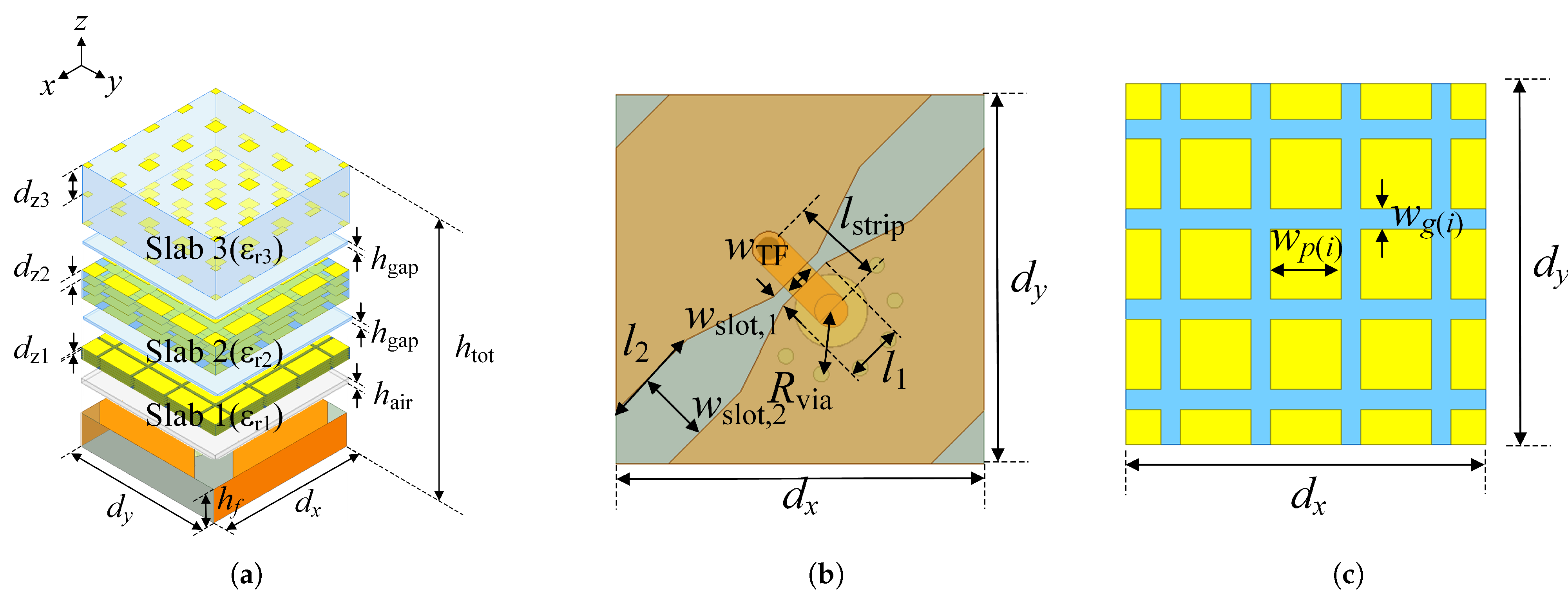
Figure 1a illustrates the proposed array element, with ADLs integrated above a slot feeder. The slot feeder with dimensions of
×
= 8.33 mm × 8.33 mm is printed on a dielectric substrate with
= 2.2, tan
= 0.0009, and a height of
h = 5.56 mm. The antenna size
(=
) corresponds to a half-wavelength at the maximum operating frequency of 18 GHz. Each slab stacked above the slot feeder consists of multiple ADLs with individual thicknesses of
,
, and
, with the number of layers of
,
, and
. Moreover, there are gaps between the different slabs, denoted as
= 0.13 mm, to ensure electrical isolation between patches of the different slabs. Note that the guided mode in the slabs undergoes different multipath lengths along the
x- and
y-directions due to the different boundary conditions of a 1-D connected array in the
- and
-planes. This introduces a 90° phase difference between the vertical and horizontal
E-field components. From Slab 1 to Slab 3, the effective permittivities of the slabs are designed to decrease monotonically (i.e.,
>
>
). The gradient effective permittivities facilitate a gradual impedance transition from the guided mode (in Slabs 1–3) to the radiating mode (above Slab 3), thereby enabling wideband impedance matching and CP performance. An air gap with a thickness of 0.25 mm is introduced between the slot and Slab 1 to suppress surface waves along the
-plane.
Figure 1b presents the geometry of the slot feeder with design parameters. The slot feeder consists of a slot on the top, a 50-
vertical microstrip transition, and a bottom ground. The side walls designed in the
-plane form a cavity to improve port isolation. The bow-tie slot, with tapered gaps from
to
, is employed to broaden impedance bandwidth, and it is rotated by 45° to produce a slant-polarized wave with an identical
E-field along the
x- and
y-directions. The slot is excited by a vertical microstrip transition with a trace width of
= 0.75 mm and a length of
= 2 mm. The vertical transition has a surrounding of posts with a diameter of 0.35 mm to prevent unwanted field leakage, and it is connected to an SMPM connector. The distance between the center and the surrounding posts (
) is adjusted for optimum impedance matching. As shown in
Figure 1c, the ADL of each dielectric slab consists of periodic metallic patterns. In our antenna design, all ADLs have the same periodicity of
+
= 2.08 mm. The gap between the patches
of each slab is adjusted to control the series capacitance, resulting in a distinct effective permittivity. The design parameters used in this work are presented in
Table 1.
Figure 2 shows the operating principle of the proposed antenna. As shown in
Figure 2a, the wave reflects at the boundaries in the
- and
-planes during propagation through ADLs due to the difference in relative permittivities between the slab and the air. Since the proposed structure is periodic only in the
x-direction, the propagating guided waves experience different multipath lengths along the
x- and
y-directions. This leads to a phase difference between the
and
components, which becomes larger as the wave propagates along the +
z direction. Assuming that
and
are the same, then the antenna will have a circular polarization when the phase difference becomes 90°.
Figure 2b shows the dispersion diagrams of the three slabs in the proposed design. The dispersion diagrams are analyzed by using a numerical simulation, Ansys HFSS [
24]. In the simulation, each slab is analyzed as an infinite array condition with two Floquet ports in the
-planes. It is shown that all slabs exhibit slow-wave propagation across the target operating frequency band (12–18 GHz), indicating that the wave is effectively guided in the slab as a dielectric slab waveguide.
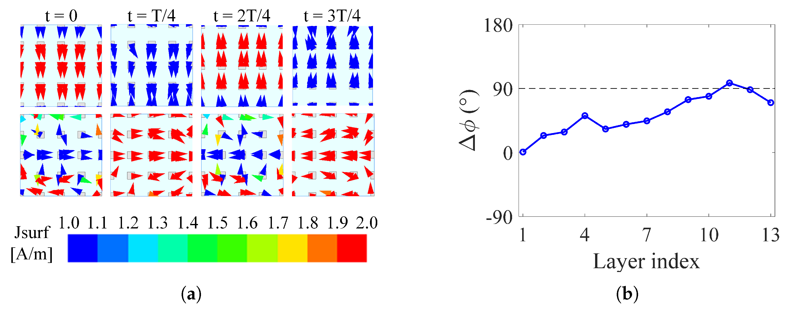
Figure 3a shows the surface current distribution observed on the top ADL. In the simulation, two orthogonal (
y- and
x-polarized) waves are individually excited by connected arrays with
y- and
x-polarization. Then, the responses of the ADLs are observed according to the polarization of the incident waves. For both
y- and
x-polarized wave excitations, the top ADL shows linearly polarized current distributions. Moreover, the vector of the currents indicates a phase delay of 90° between the
y- and
x-polarized wave incidence with similar amplitudes from
t = 0 to
t = 3T/4. This means RHCP waves will be produced when the
y- and
x-polarized waves are incident on the ADLs simultaneously.
Figure 3b presents the phase difference (
) between the surface currents in the
x- and
y-directions. The surface currents of the center element on the top ADL are observed. As multiple layers are stacked on the slot feeder, the phase difference gradually increases from 0.74° to 97.84°. When 12 ADLs, including two dielectric substrate gaps, are stacked on the feeder,
becomes 90°, implying that the radiating
E-field becomes CP. Note that each slab exhibits dispersion as the number of layers increases. Therefore, the number of layers in each slab is determined to avoid the dispersion while ensuring a specific height for achieving CP properties.
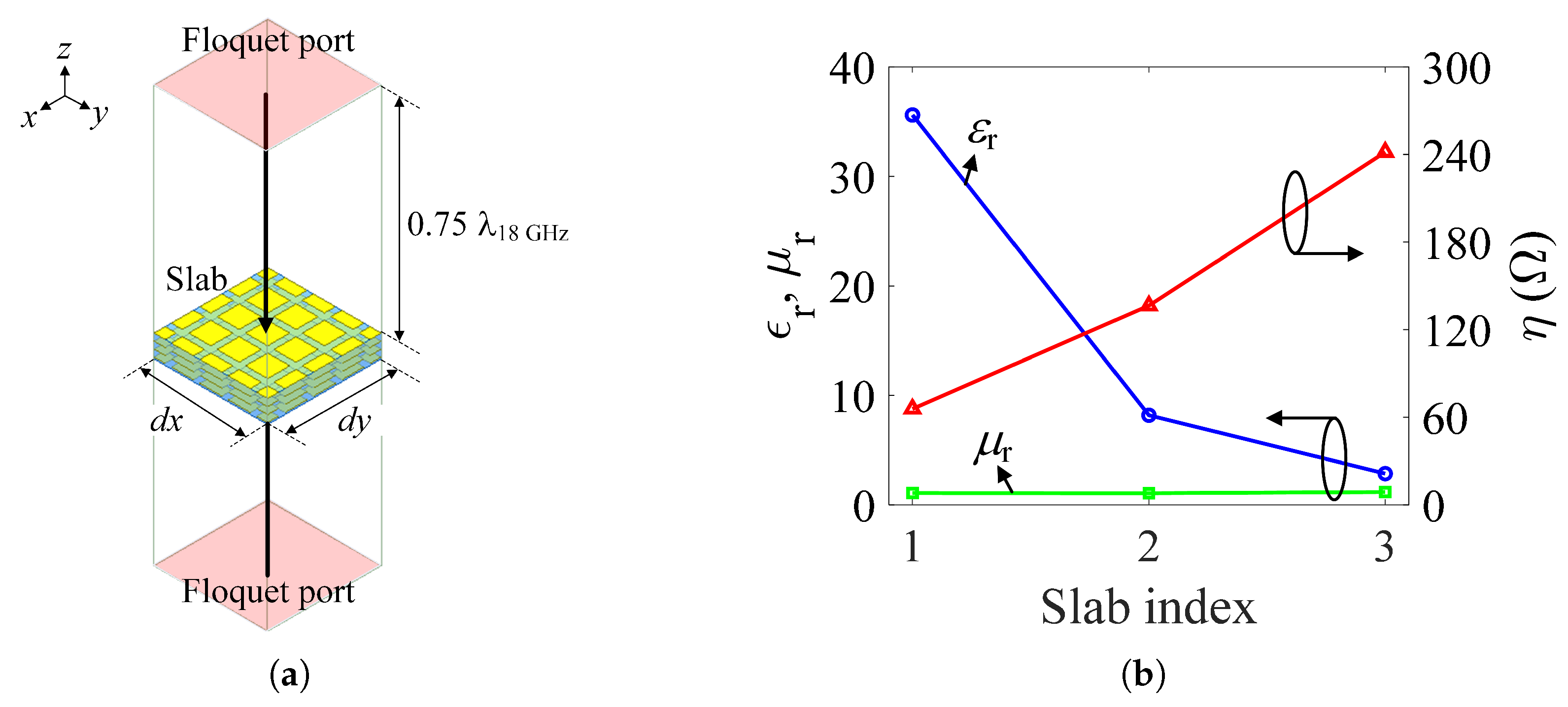
Figure 4 shows the design process of the gradient ADLs. For wideband impedance matching properties, the wave impedance (
) needs to be transformed from the slot antenna impedance to the intrinsic impedance (377
). Hence, the slabs are designed to have gradual impedance variations. As per
Figure 4a, the Nicolson–Ross–Weir (NRW) method is used to estimate the wave impedance of each slab by assuming an infinite array condition with Master/Slave periodic boundaries and a Floquet port [
25]. De-embedding is applied in both the
- and
-directions to compensate for the propagation in the air. The optimized relative permittivity (
), relative permeability (
), and corresponding
for the slabs are presented in
Figure 4b, where
. Since the slot feeder exhibits
= 63.75
, the (
) of Slab 1 is designed to have 65.76
with
= 35.6 to minimize the boundary reflection between them. Additionally, Slabs 2 and 3 have
= 136
and
= 241
with
= 8.18 and
= 2.86, respectively. This design approach enables a gradual impedance transition from the slot impedance to free space, which is effective for wideband properties.
Figure 5 presents the antenna performance enhancement as the number of ADL slabs increases. In
Figure 5a, the active S-parameters are calculated as (
1).
where
N is the number of array elements, and
denotes the complex array weights applied to the
nth element for the steering angle
. The impedance matching is improved within the target frequency range when increasing the number of slabs. When the number of slabs is more than two, wideband properties are observed. As depicted in
Figure 5b, the antenna with three slabs shows an AR of less than 3 dB across the operating frequency range, while the antenna without slabs shows an AR of over 10 dB. Moreover, the boresight gain in
Figure 5c increases as the number of slabs increases, with an improvement of up to 1.62 dB compared to the antenna without slabs.
3. Fabrication and Measurement
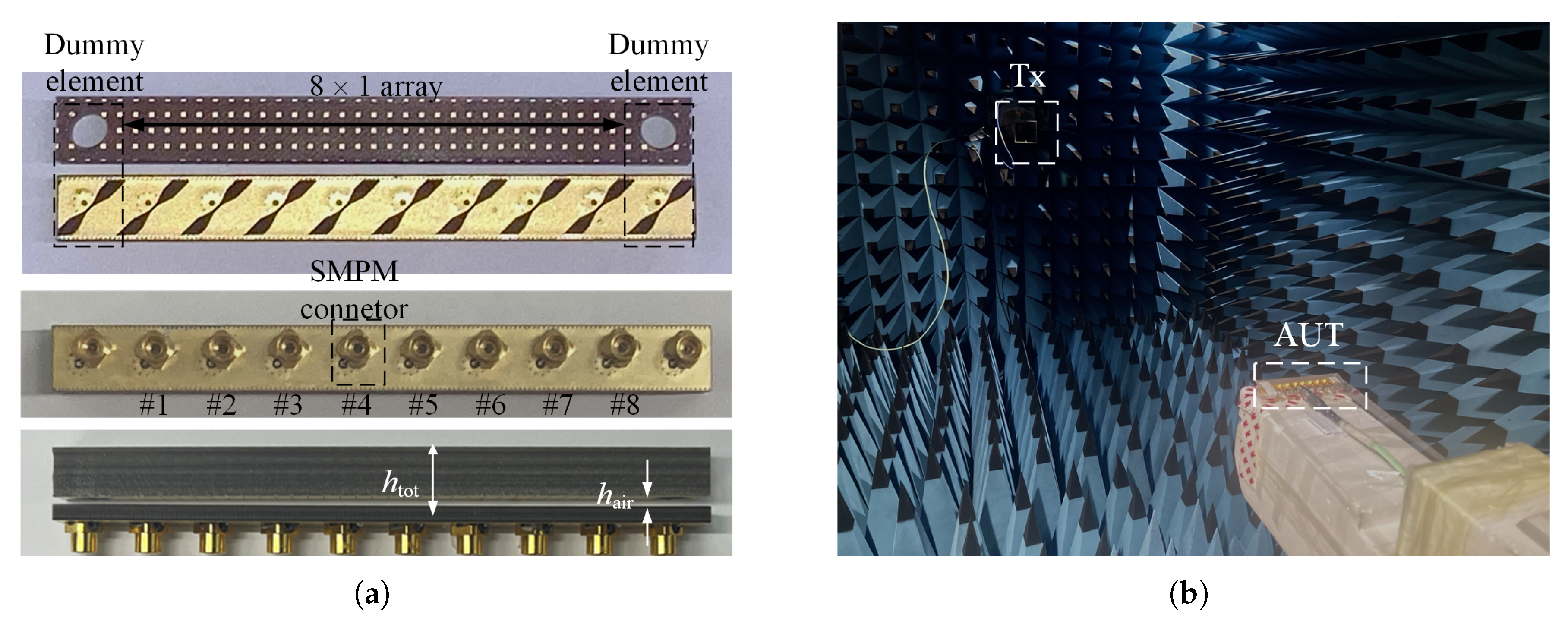
An 8 × 1 array is fabricated using a Taconic TLY-5 substrate (
= 2.2, tan
= 0.0009), as shown in
Figure 6a. The center-to-center distance between each port is 8.33 mm (0.5
), and the total array aperture is 66.64 mm × 8.33 mm (4
× 0.5
). The total height of the antenna is
= 7.64 mm. The metal part at the corner of the fabricated antenna was introduced to realize the side walls for port isolation using multiple posts and metallic strips. To mitigate the performance degradation of the edge array elements, dummy elements are implemented at both ends, terminated with 50-
loads. The antenna is excited using an SMPM connector. Moreover, there are two screw holes in the dummy elements to support the entire antenna structure, and foam is added between Slab 1 and the slot feeder for an air gap of
= 0.25 mm. The matching characteristics, radiation patterns, and ARs of the fabricated array antennas are measured in an anechoic chamber, as in
Figure 6b.
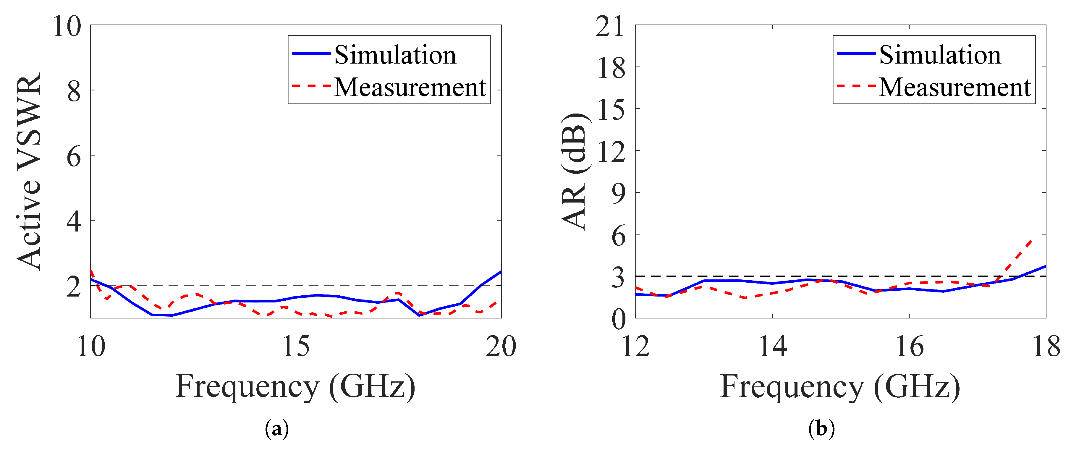
Figure 7a shows the simulated and measured active VSWR of the proposed antenna. In the simulation, the finite-element method (FEM) in Ansys HFSS is used. In the measurement, the fourth array element is measured while the other elements are terminated with 50-
loads. The proposed antenna exhibits a simulated impedance bandwidth of 9 GHz (10.5–19.5 GHz) and a measured bandwidth of 9.8 GHz (10.2–20 GHz).
Figure 7b presents the simulated and measured AR. The measured AR bandwidth is 5.5 GHz (12–17.5 GHz), and the simulated AR bandwidth is 5.2 GHz (12–17.2 GHz).
The AEPs of the proposed antenna are measured by exciting the ports under testing while terminating the other ports with 50-
loads.
Figure 8 presents the AEPs of the fourth element. The measured boresight gain is 3.03 dBic at 12 GHz and 9.63 dBic at 18 GHz. The simulated gain is 4.08 dBic and 7.02 dBic at 12 GHz and 18 GHz, respectively. The measured AEPs exhibit more gain fluctuation compared to the simulated results. The discrepancies between the simulated and measured AEPs can be attributed to the following reasons. (1) The air gap is not uniform across all ports due to the irregular foam surface; (2) The use of adhesive material during the fixation of the multiple ADLs affects the effective permittivities; (3) The jig used for antenna measurement contributes to these discrepancies. Among them, the nonuniform air gap between Slab 1 and the slot feeder is the main cause for such a difference. Due to the low rigidity and uneven surface condition of the foam, the array has nonuniform air gaps across all elements, causing fluctuation in boresight gain.
From the measured AEPs of eight array elements, the RHCP beam pattern of the proposed array is synthesized, as plotted in
Figure 9. Overall, the simulated results are in good agreement with the measured results. The simulated maximum boresight gain and side lobe level (SLL) are 13.18 dBic and 14.72 dB, respectively, while the measured results are 12.69 dBic and 12.05 dB. At 14 GHz, the simulated and measured maximum boresight gains are 13.87 dBic and 13.63 dBic. At 17 GHz, the simulated and measured maximum boresight gains are 15.23 dBic and 15.74 dBic, respectively, with an SLL of 12.97 dB in the simulation and 10.76 dB in the actual measurement. There were discrepancies in the SLLs of the synthesized beam patterns at 14 and 17 GHz due to fabrication errors, including misalignment between the signal trace and the SMPM connector in the soldering process and uneven air gaps.
The measured AEPs were further applied to a broadband frequency-invariant beamforming algorithm, which equalizes the element excitations over a frequency to maintain a constant half-power beamwidth (HPBW). To implement the FIB algorithm on the proposed array antenna, it is necessary to derive the corresponding FIB weights. To derive the desired FIB weights, the discrete Fourier transform (DFT) method proposed in [
26] was employed. The desired radiation pattern was determined beforehand for the DFT process. The desired pattern can take the form of any arbitrary function, such as the bandpass filter expressed in (
2):
where
N is the size of the filter, and
represents the
n-th coefficient of the bandpass filter. Under the assumption of an infinite antenna array distributed along the
x-axis, the beam response,
, can be expressed as a sum of exponential phase terms multiplied by the FIB weight
, as shown in (
3).
where
represents the inter-element spacing,
denotes the angular frequency,
m is an antenna index, and
c is the speed of light. By substituting
with
, the beam response can be expressed in the form of DFT as
The desired FIB weights,
, are obtained by applying the inverse DFT for
frequency samples as
where
=
2
. As
typically exceeds the actual number of array elements
M, a rectangular window is employed to extract a subset of
M weights from the total
samples.
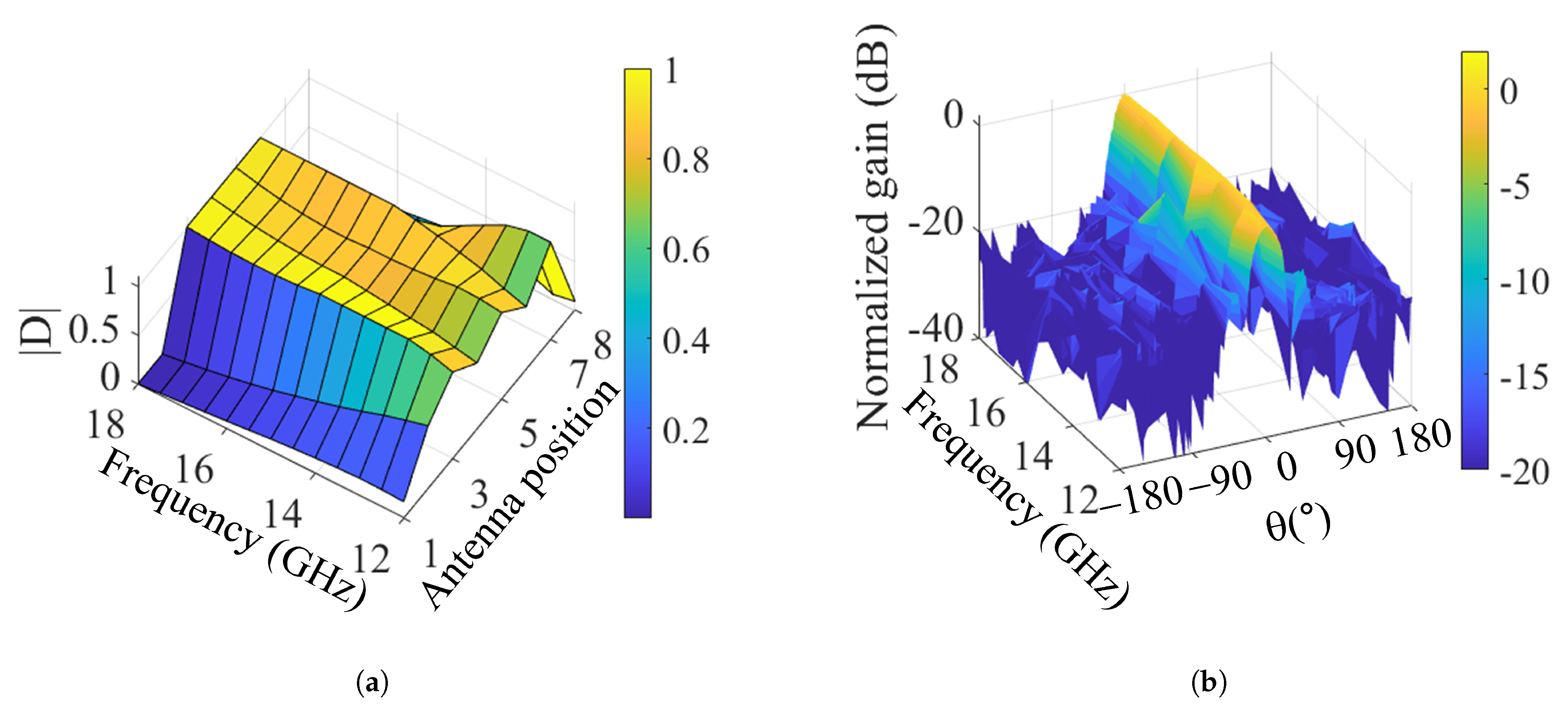
Figure 10a shows the magnitude of the FIB weight
for each element of the array across 12 GHz to 18 GHz. As in the figure, the FIB weight applied to each antenna element varies with frequency. Note that FIB weights are concentrated on the central eight elements, even when the large array elements are used. Thus, the effect of truncation error is negligible in the FIB implementation using the proposed array with eight elements. The derived array weights are applied to the measured AEPs to produce a frequency-invariant beam pattern, as shown in
Figure 10b. The FIB pattern derived from the measured AEPs successfully achieves an average HPBW of 24.77° with a standard deviation below 3.63° across the operating frequency band, demonstrating the FIB implementation using the proposed array.
Table 2 compares the proposed array antennas with previous CP antennas. Although the antennas reported in [
8,
14,
15] offer lower profiles than our work, the proposed array antennas show wider impedance and 3 dB AR bandwidths, with moderate boresight RHCP gain. The antenna suggested in [
11] shows much wider impedance and AR bandwidths; however, it requires a larger array dimension compared to our design. Moreover, in [
8] and [
11], dual ports or feeding networks are adopted for CP radiation, which increases design complexity. On the other hand, the proposed 1-D connected array requires simple slot feeders for excitation, and CP generation is achieved based on the different boundary conditions of a 1-D connected array, which has not been investigated in previous works. In addition, wideband matching properties are realized using multiple ADLs with gradient effective permittivities for a gradual impedance transition. This wideband CP property using a 1-D array enables consistent EW performance in modern aircraft with spatial constraints.
