1. Introduction
With the advancement of the space industry, satellite-based communication technology has become a core technology in various fields, including military intelligence gathering, disaster monitoring, climate observation, and the construction of global network infrastructure [
1]. Given the increasing demand for high integration density in modern satellite systems, ensuring stable operation under harsh radiation environments has become a critical design challenge. To ensure the stable operation of such systems in extreme space environments, it is crucial to employ memory devices that can maintain data integrity even under radiation exposure. Among various memory technologies, static random-access memory (SRAM) has been widely utilized in space applications due to its fast access speed, high integration density, and low power consumption [
2].
However, unlike terrestrial environments, outer space continuously exposes semiconductor circuits such as SRAM to high-energy particle radiation, making them highly susceptible to soft errors. When a high-energy particle strikes a reverse-biased junction in a semiconductor, electron–hole pairs are generated. If these carriers accumulate at a sensitive node, they induce a short voltage pulse known as a single-event transient (SET) [
3]. When the amplitude of this pulse exceeds the threshold voltage of the node, it can flip the stored data, resulting in a SEU [
4]. The threshold voltage refers to the minimum gate voltage required to turn on a transistor. Moreover, as CMOS process technology continues to scale down and the spacing between transistors becomes narrower, charge-sharing effects are exacerbated. Consequently, a single particle strike can affect multiple nodes simultaneously, leading to SEMNUs [
5].
To mitigate these radiation-induced faults, several circuit-level techniques, such as error correction codes (ECC) and radiation-hardened by design (RHBD), have been employed. ECC detects and corrects errors through encoded data structures, but the inclusion of encoding and decoding logic increases circuit complexity and computational delay [
6]. In contrast, RHBD enhances circuit resilience by structurally optimizing the topology to provide internal recovery paths in the event of SEUs or SEMNUs [
7]. This approach is considered a more practical solution, as it ensures the high reliability required in space while minimizing area and power overhead.
In this paper, we adopt an RHBD-based approach to mitigate the impact of SEUs and propose the EWS-16T cell, which offers high write performance and low power characteristics. The proposed cell comprises 16 transistors and includes two storage nodes (Q and QB) and two internal nodes (S0 and S1). By separating the write path from the storage path and minimizing the number of sensitive nodes, the EWS-16T achieves high operational reliability. In particular, Q and S0 are designated as sensitive nodes, and the design allows for self-recovery from SEUs occurring at a single node. Although recovery is limited when both sensitive nodes are simultaneously struck, the cell layout ensures sufficient spacing between transistors to reduce the likelihood of charge-sharing-induced SEMNUs. Furthermore, the proposed cell demonstrates the best write performance, the shortest write access time, and the lowest hold power consumption among all compared cells [
8,
9,
10,
11,
12].
EWS-16T distinguishes itself from previous designs, such as SAW16T and RHSCC16T, by optimizing radiation tolerance and improving write performance while minimizing power consumption. Unlike SAW16T, which struggles with SEMNU recovery and high power consumption, and RHSCC16T, which faces significant area and power overheads, EWS-16T offers superior efficiency by separating the write path from the storage path, reducing sensitive nodes, and enhancing reliability without the drawbacks of increased complexity or power usage. This makes EWS-16T a more efficient and practical solution in radiation-prone environments.
The rest of this paper is organized as follows.
Section 2 describes the design, basic operation, and self-recovery mechanisms for SEUs and SEMNUs of the proposed EWS-16T cell.
Section 3 presents the comparative analysis with existing SRAM cells. Finally,
Section 4 concludes the paper.
2. Proposed EWS-16T SRAM Cell
2.1. Design and Operation of the EWS-16T Cell
Figure 1 illustrates the circuit schematic of the proposed EWS-16T SRAM cell, and
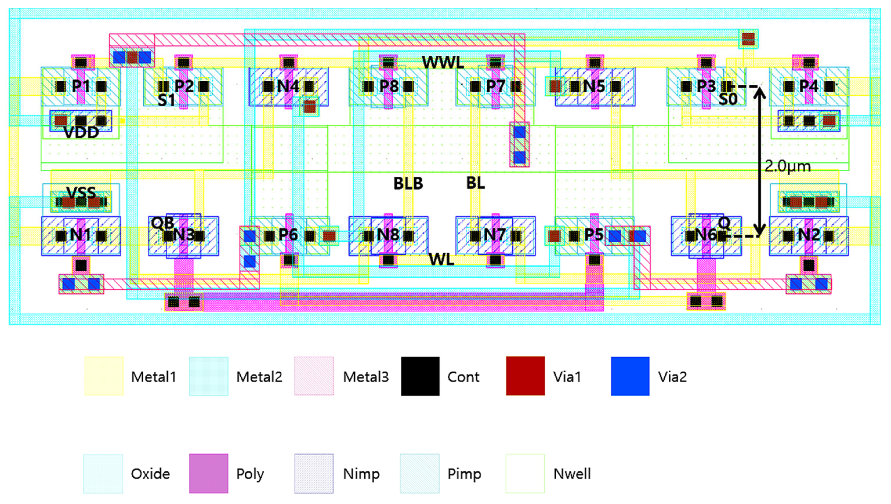
Figure 2 presents its corresponding layout. The EWS-16T cell is designed with a dual-access architecture to enhance write performance while maintaining high radiation tolerance. It comprises two storage nodes (Q and QB) and two internal nodes (S1 and S0). Transistors P7 and P8 are controlled by the write word line (WWL) and connect the internal nodes S1 and S0 to the bit lines BL and BLB, respectively. Meanwhile, transistors N7 and N8 are controlled by the word line (WL) and connect the storage nodes Q and QB to the bit lines BL and BLB. When the stored data in the cell represents logic ‘1’, nodes Q and QB hold logic values of ‘1’ and ‘0’, respectively, and internal nodes S0 and S1 store logic values of ‘0’ and ‘1’. This complementary storage structure allows robust data retention and controlled feedback operation within the cell.
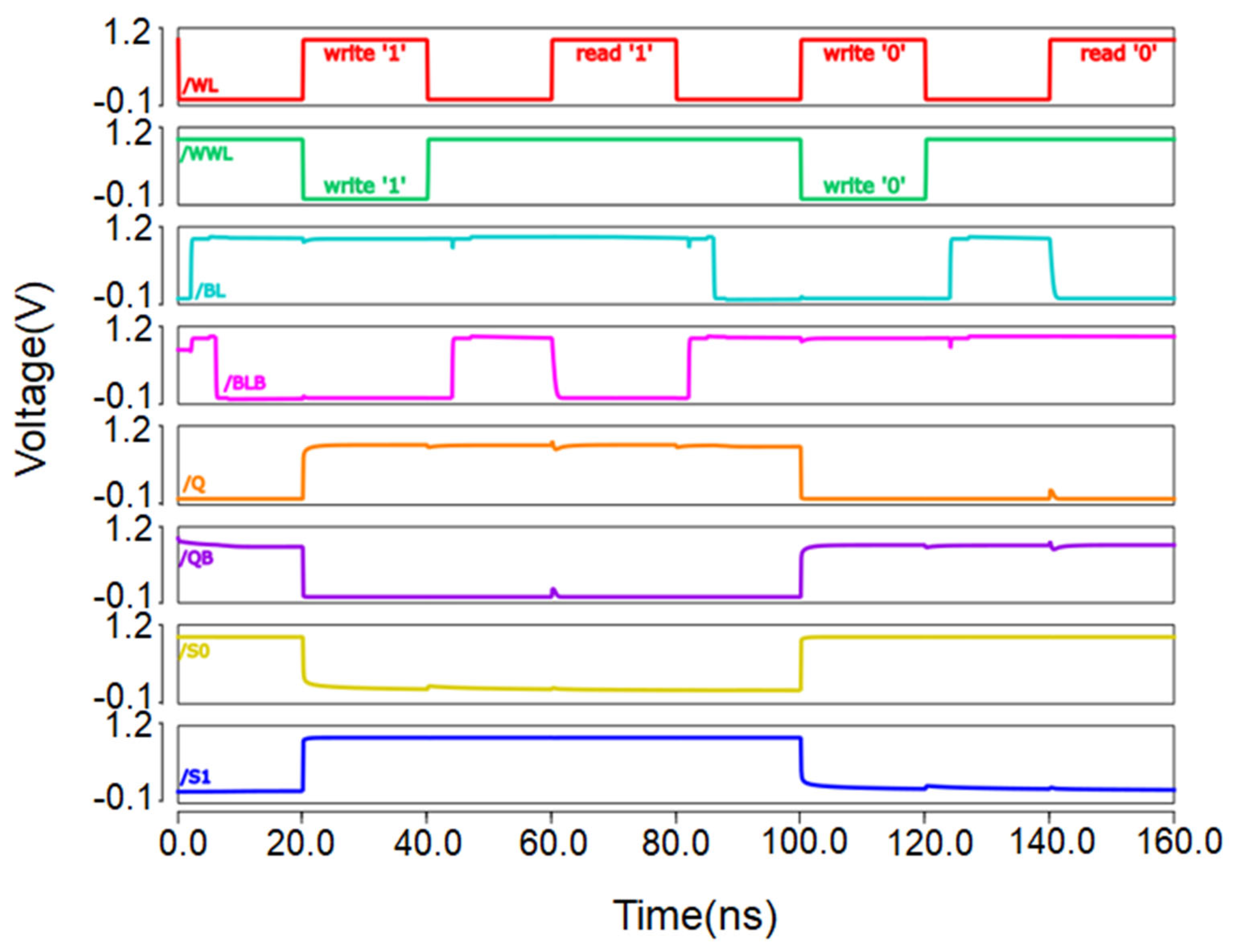
Figure 3 presents the transient waveforms of the EWS-16T cell under hold, read, and write operations, confirming stable functionality under typical conditions. The detailed behaviors of each operation mode are explained below.
2.1.1. Hold Operation
During the hold operation, WL and WWL are deactivated, keeping all access transistors turned off. The bit lines BL and BLB are maintained at VDD to reduce wake-up time. Assuming an initial logic state of ‘1’, transistors N2, N3, N5, P2, P4, and P6 are turned on, while the remaining transistors remain off. As a result, the originally stored data in the EWS-16T cell remains unchanged and is reliably retained.
2.1.2. Read Operation
During the read operation, the bit lines BL and BLB are precharged to VDD. WL is set to VDD to activate access transistors N7 and N8, while WWL is also set to VDD to deactivate access transistors P7 and P8. In this configuration, the voltage of BL remains unchanged, but BLB can be discharged through transistors N3 and N8. When the voltage difference between BL and BLB exceeds approximately 50 mV, the sense amplifier can accurately determine the stored logic value.
2.1.3. Write Operation
To write a logic ‘1’ into the cell, BL is pre-discharged to VDD, and BLB is precharged to GND. WL and WWL are set to VDD and GND, respectively, turning on all access transistors connected to the internal and storage nodes. As a result, nodes Q and S1 are charged through transistors N7 and P8, respectively, while nodes QB and S0 are discharged through transistors N8 and P7. As the voltages of Q and S1 increase, the pull-up paths for QB and S0 become weakened, facilitating the rapid discharge of QB. When the voltage of QB drops below the threshold voltage of the NMOS transistor, the pull-down transistor N6 turns off, further accelerating the charging of node Q. The storage node QB is weakly held at logic ‘1’ by the surrounding NMOS transistors, while the internal node S1 is weakly held at logic ‘0’ by the surrounding PMOS transistors. These weakly driven nodes can be easily overridden by the strongly driven access paths, thereby improving the write efficiency of the proposed EWS-16T cell.
2.2. SEU Recovery Analysis
This section analyzes the impact of SEUs on the EWS-16T cell and evaluates its inherent self-recovery capabilities. A node is classified as sensitive if it is vulnerable to state alteration due to SEU-induced transient pulses. It is widely known that SEUs induce negative transient pulses in NMOS transistors and positive transient pulses in PMOS transistors. Specifically, when a radiation particle strikes an NMOS transistor, it can cause a transient transition of either “1” → “0” or “0” → “0”, depending on the node’s logic value. In contrast, a PMOS transistor typically experiences “1” → “1” or “0” → “1” transitions [
13].
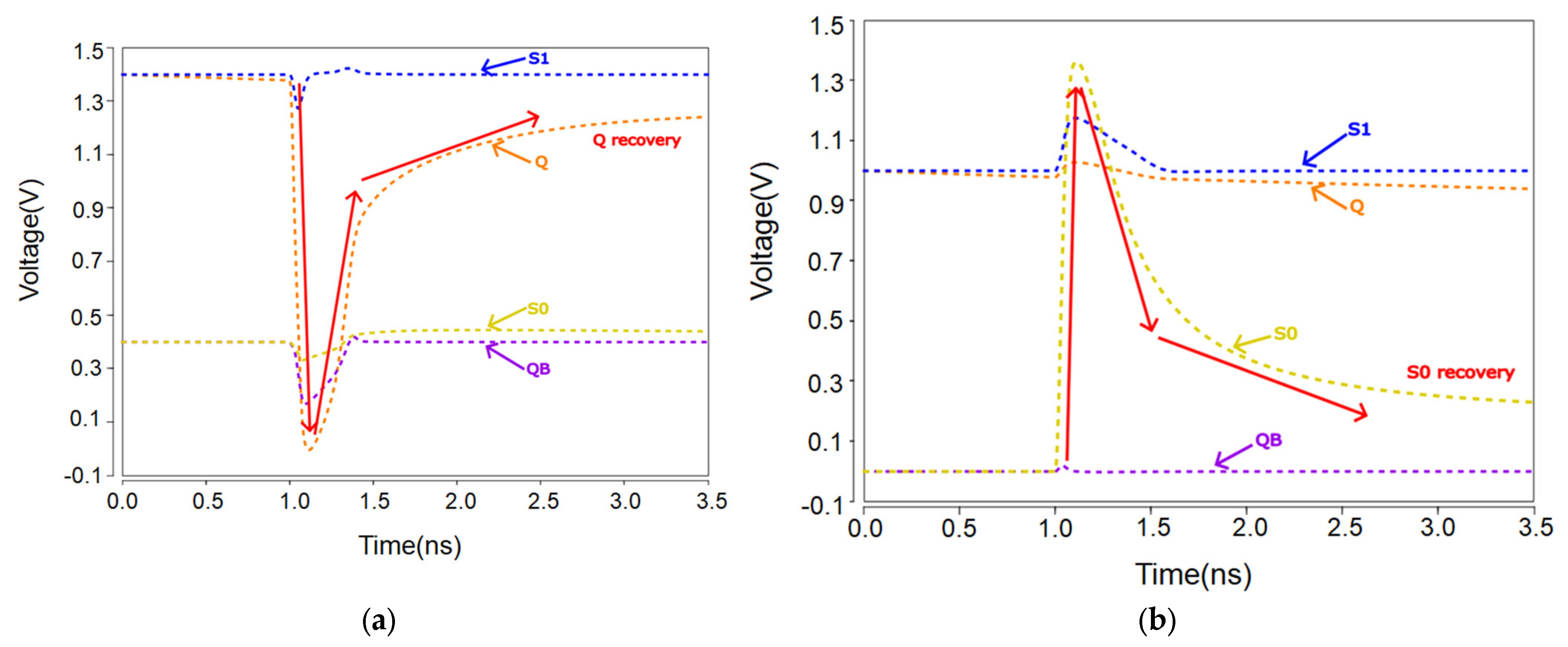
Therefore, a node storing logic ‘1’ and surrounded by NMOS transistors, or a node storing logic ‘0’ and surrounded by PMOS transistors, is considered to be SEU-sensitive. When node Q holds logic ‘1’ in the EWS-16T cell, its complementary node QB stores logic ‘0’ and is exclusively connected to NMOS transistors. This configuration permits only a “0” to “0” transition at QB, making it inherently immune to state flipping and thus classified as a non-sensitive node. Likewise, the internal node S1 retains logic ‘1’ and is surrounded by PMOS transistors, allowing only a “1” to “1” transition. S1 is therefore also considered non-sensitive. Q holds logic ‘1’ while being connected to NMOS transistors, and S0 stores In contrast, Q holds logic ‘1’ and is connected to NMOS transistors. S0 stores logic ‘0’ and is connected to PMOS transistors. This configuration satisfies the condition under which SEUs can induce logic inversion, thus classifying Q and S0 as sensitive nodes. The transient responses and recovery behaviors at these sensitive nodes are illustrated in
Figure 4, demonstrating the EWS-16T cell’s ability to self-recover from SEU-induced perturbations.
2.2.1. SEU at Node Q
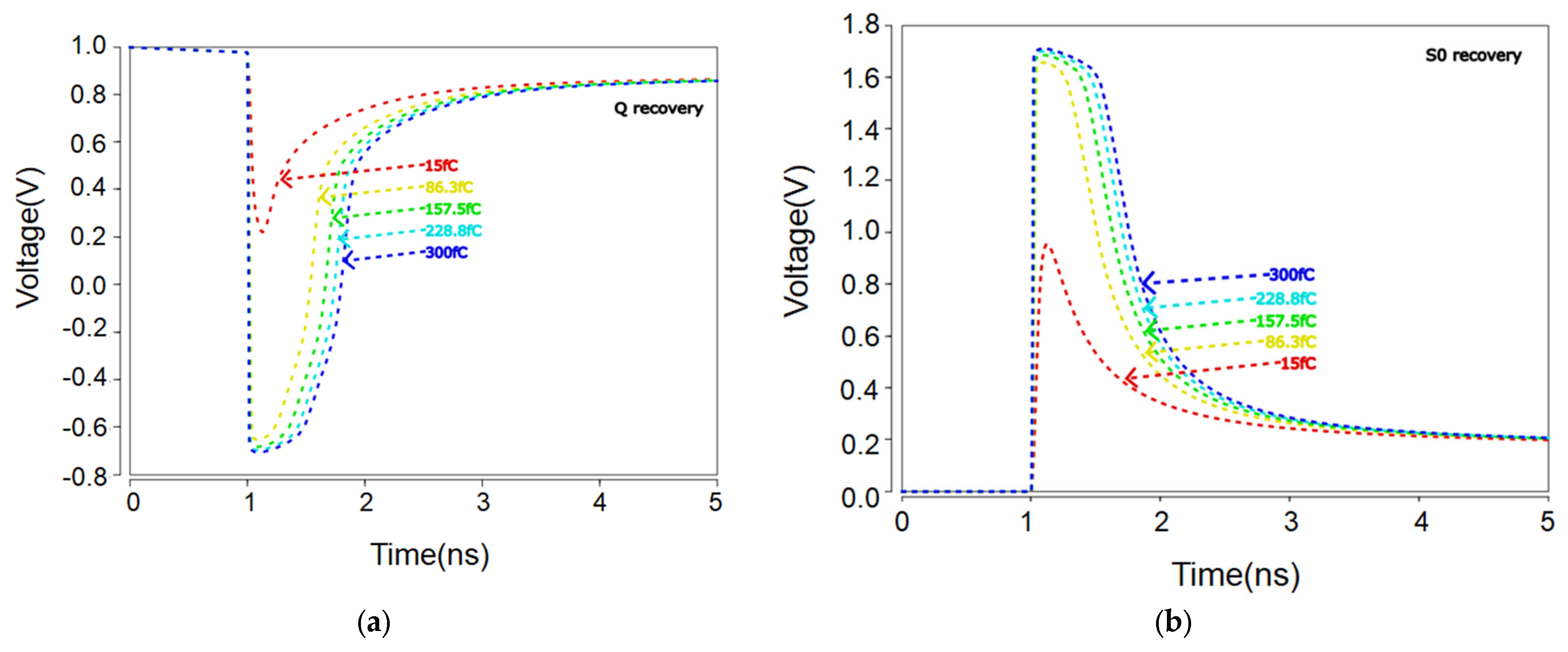
When an SEU causes node Q, initially storing logic ‘1’ to flip to ‘0’, transistor P5 turns on and N3 turns off. Transistors P1 and N1 remain off, while P5 remains active. As a result, the states of nodes QB and S1 remain unchanged, and node S0 is unaffected. Consequently, P4 and N2 remain on, while N6 remains off. Therefore, node Q is successfully restored to its original state through the feedback loop, demonstrating self-recovery. This self-recovery behavior of node Q is further illustrated in the transient response shown in
Figure 5a, where the voltage level of Q initially drops due to the SEU but is successfully restored through the feedback loop.
2.2.2. SEU at Node S0
If node S0, initially storing logic ‘0’, is flipped to ‘1’ due to an SEU, transistors N1 and N4 are turned on, while P2 and P4 are turned off. However, P5 and N6 remain off. Accordingly, the states of nodes Q and S1 do not change, and QB also retains its original value. As a result, P6 and N5 are turned on, and P3 remains off. Thus, node S0 also recovers its original value via the feedback path. As shown in
Figure 5b, node S0 also exhibits self-recovery following a transient overshoot caused by the SEU, demonstrating the robustness of the proposed cell against single-node upsets.
2.2.3. SEMNU at Node Pair Q–S0
If both nodes Q and S0 are simultaneously affected by an SEMNU, resulting in transitions from “1” → “0” and “0” → “1”, respectively, transistors P5 and N4 are turned on, while P2 is turned off. This causes node S1 to discharge through P5 and N4, leading to a state change from ‘1’ to ‘0’. Subsequently, P1 turns on and remains active, allowing node Q to be recharged from ‘0’ to ‘1’ via P1 and N1. However, during this process, the internal state of the feedback loop changes, resulting in a corruption of the originally stored data. Hence, if a sufficiently large charge is deposited simultaneously at nodes Q and S0, self-recovery to the original logic state becomes impossible.
Nevertheless, it is widely recognized that charge sharing between transistors can be effectively suppressed by ensuring a minimum spacing of 1.62 µm between PMOS transistors and 0.6 µm between PMOS and NMOS transistors [
14]. As shown in
Figure 2, the proposed EWS-16T cell layout maintains a spacing of 2.0 µm between the critical node pair Q and S0, which sufficiently exceeds these minimum requirements, thereby effectively enhancing immunity to SEMNUs at this node pair. Among the six possible double-node upset combinations, five cases—those involving at least one non-sensitive node, such as Q–QB, Q–S1, QB–S0, QB–S1, and S0–S1—are inherently recoverable through the SEU self-correction mechanism. The remaining case, Q–S0, is also addressed at the layout level by ensuring sufficient node separation, thus confirming full robustness against SEMNU-like scenarios in the proposed design.
3. Implementation Results and Analysis
This section presents the simulation setup and evaluation results of the proposed EWS-16T cell, implemented using a 90 nm CMOS technology. All simulations were performed with an operating voltage of 1.0 V and an ambient temperature of 27 °C. Identical simulation conditions were applied to all evaluated cells to ensure fairness in comparison. The cell is composed of 16 transistors, and the transistor sizing is carefully optimized for enhanced write performance and power efficiency. Transistors P1–P6 and N1, N2, N4, and N5 are set to the minimum width to achieve a compact cell area. Pulldown transistors N3 and N6, which are connected to internal nodes, are sized to 1.8 times the width of their respective access transistors. Access transistors N7 and N8 are sized to 1.08 times the minimum width. Furthermore, the PMOS pull-up transistors P7 and P8, which are connected to the storage nodes, are set to 1.7 times the width of the access transistors. This sizing helps reduce the write access time and improve the charging path, thereby enhancing overall write performance.
This study presents experimental results for the read delay, write delay, WWTV, hold power, read static noise margin (RSNM), and hold static noise margin (HSNM) of the proposed EWS-16T cell. The results are compared with those of six previously reported radiation-hardened SRAM cells: QCCS [
8], SCCS [
8], SAW16T [
9], HP16T [
10], RHSCC16T [
11], and S8P8N [
12]. The transistor sizes of the comparison cells were adopted from the values reported in the corresponding references. For designs without explicitly specified dimensions, reasonable estimates were applied to ensure fair and consistent experimental conditions.
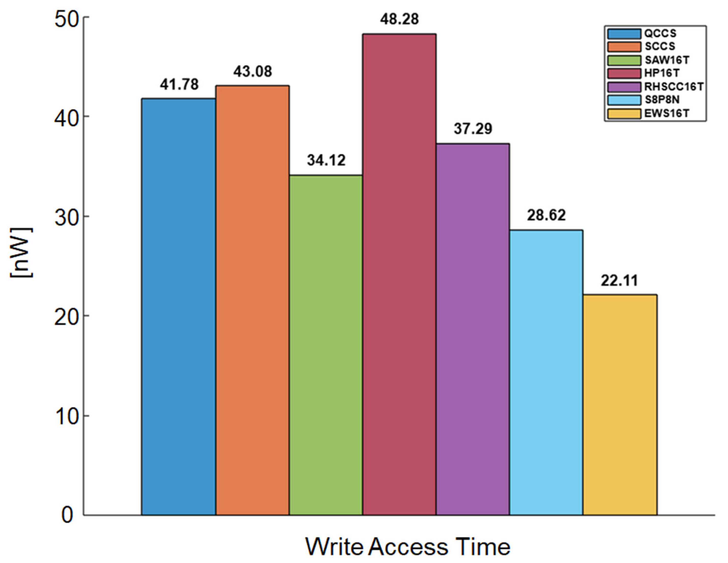
Figure 6,
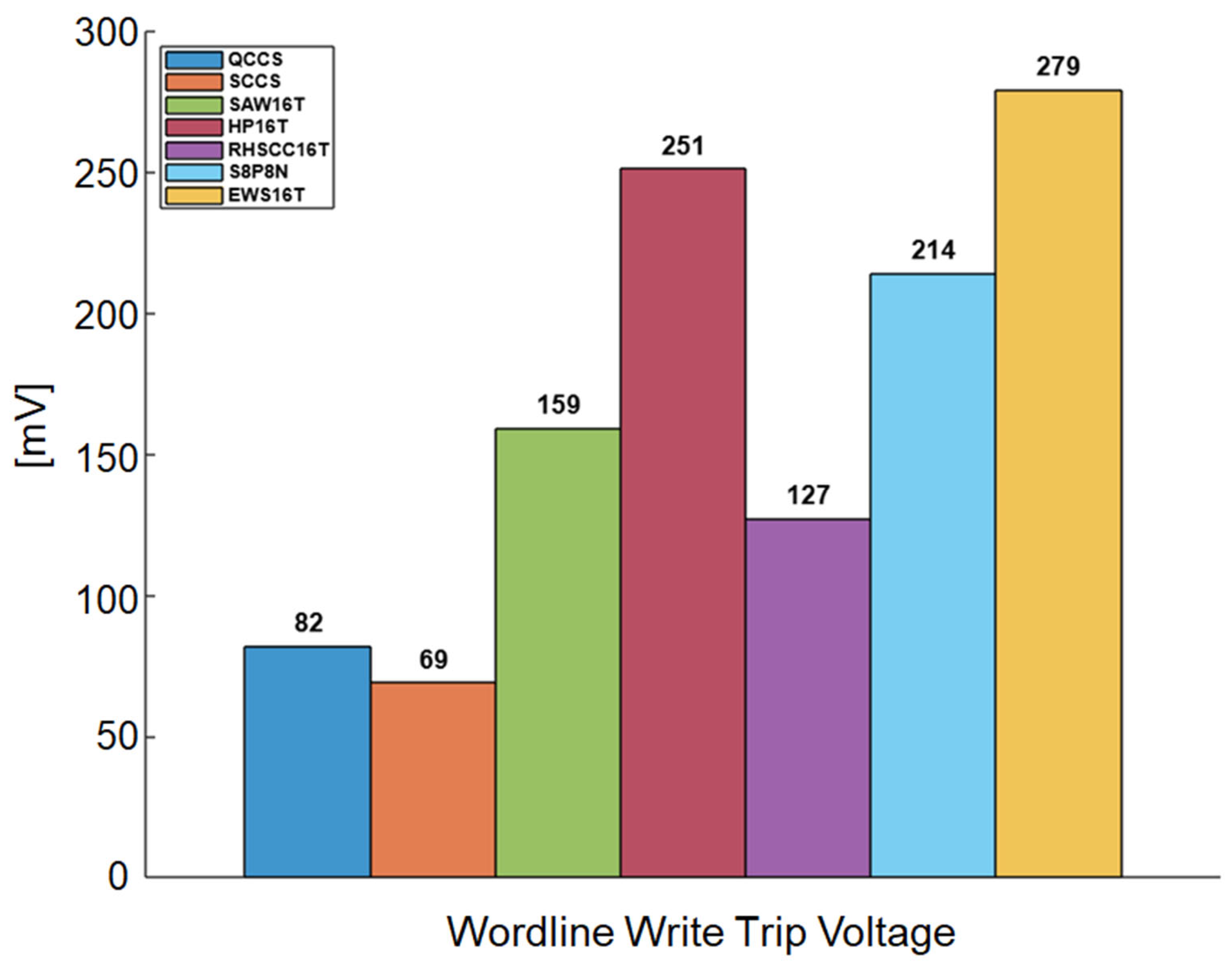
Figure 7,
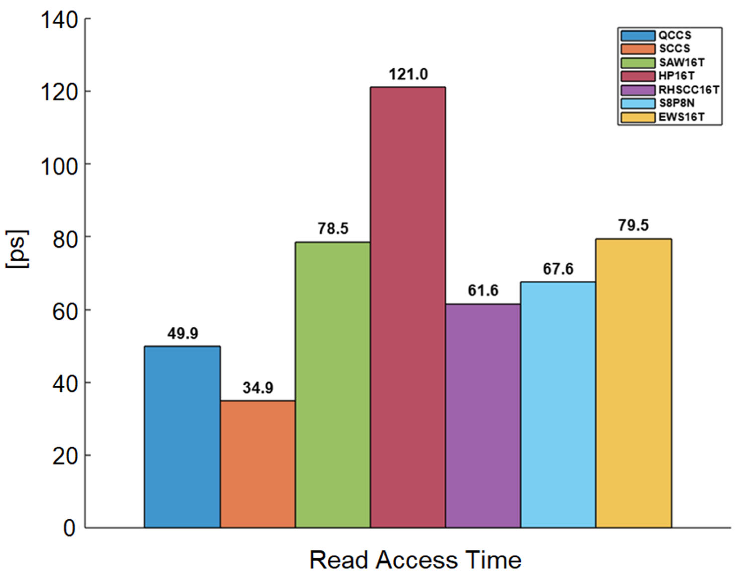
Figure 8,
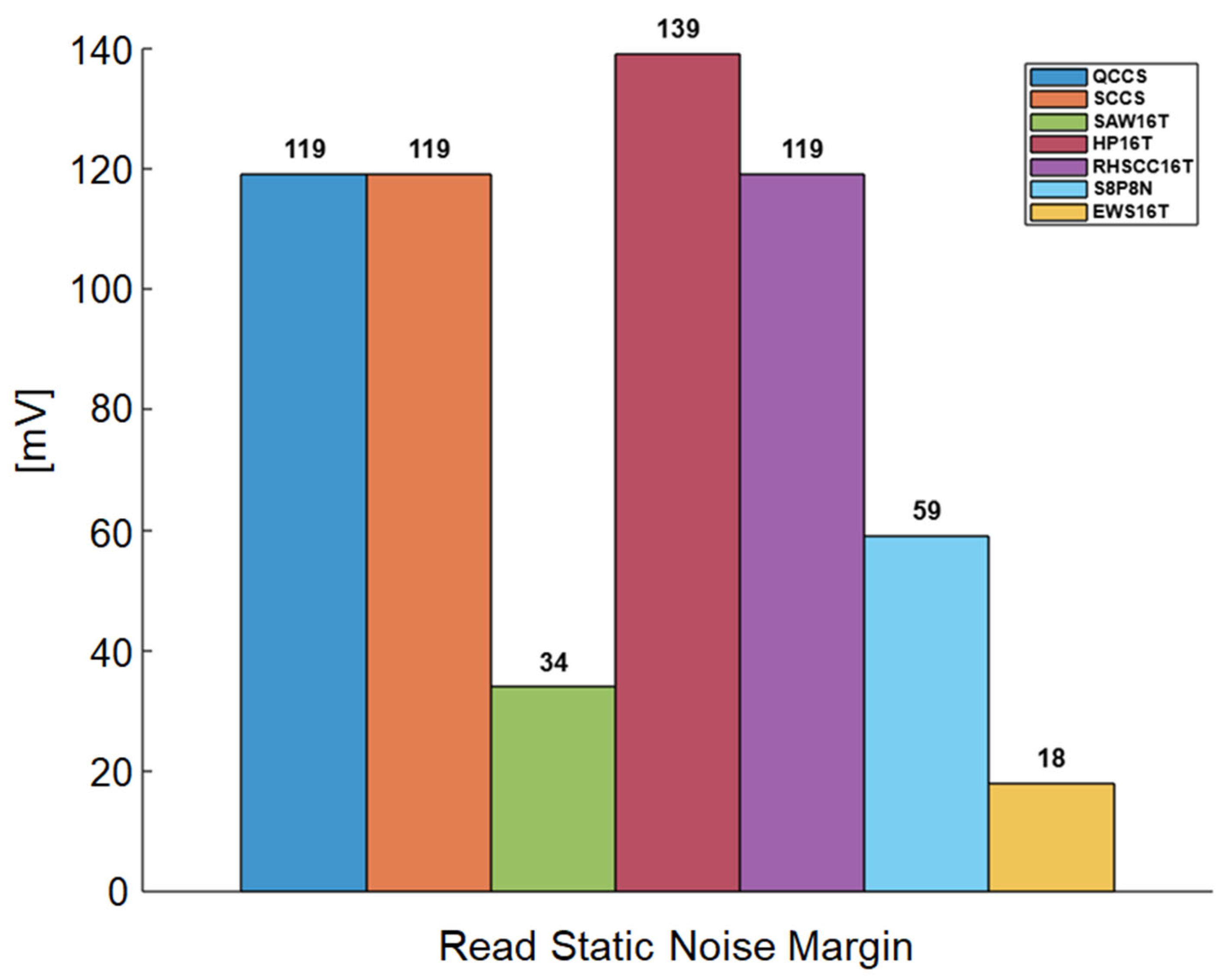
Figure 9,
Figure 10 and
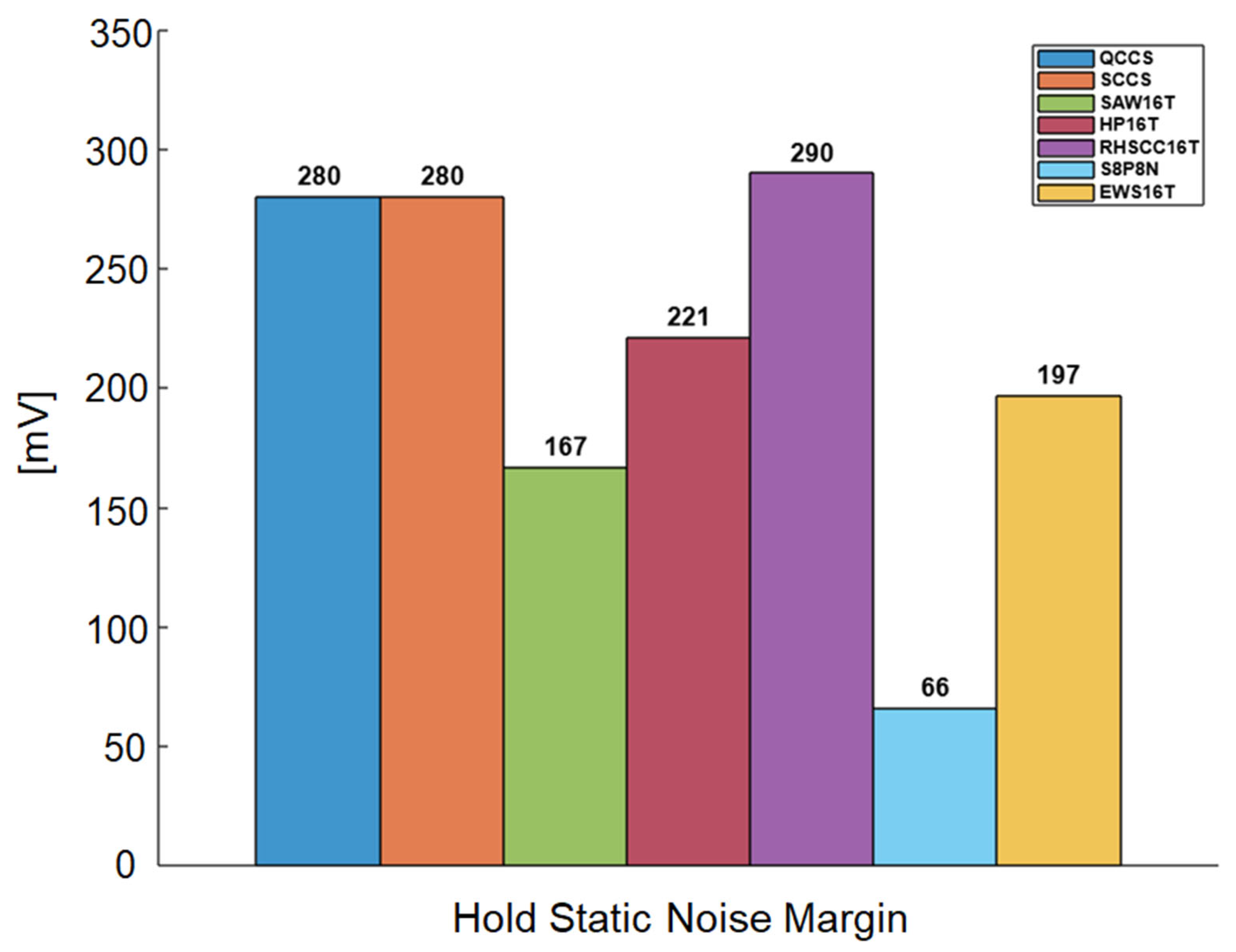
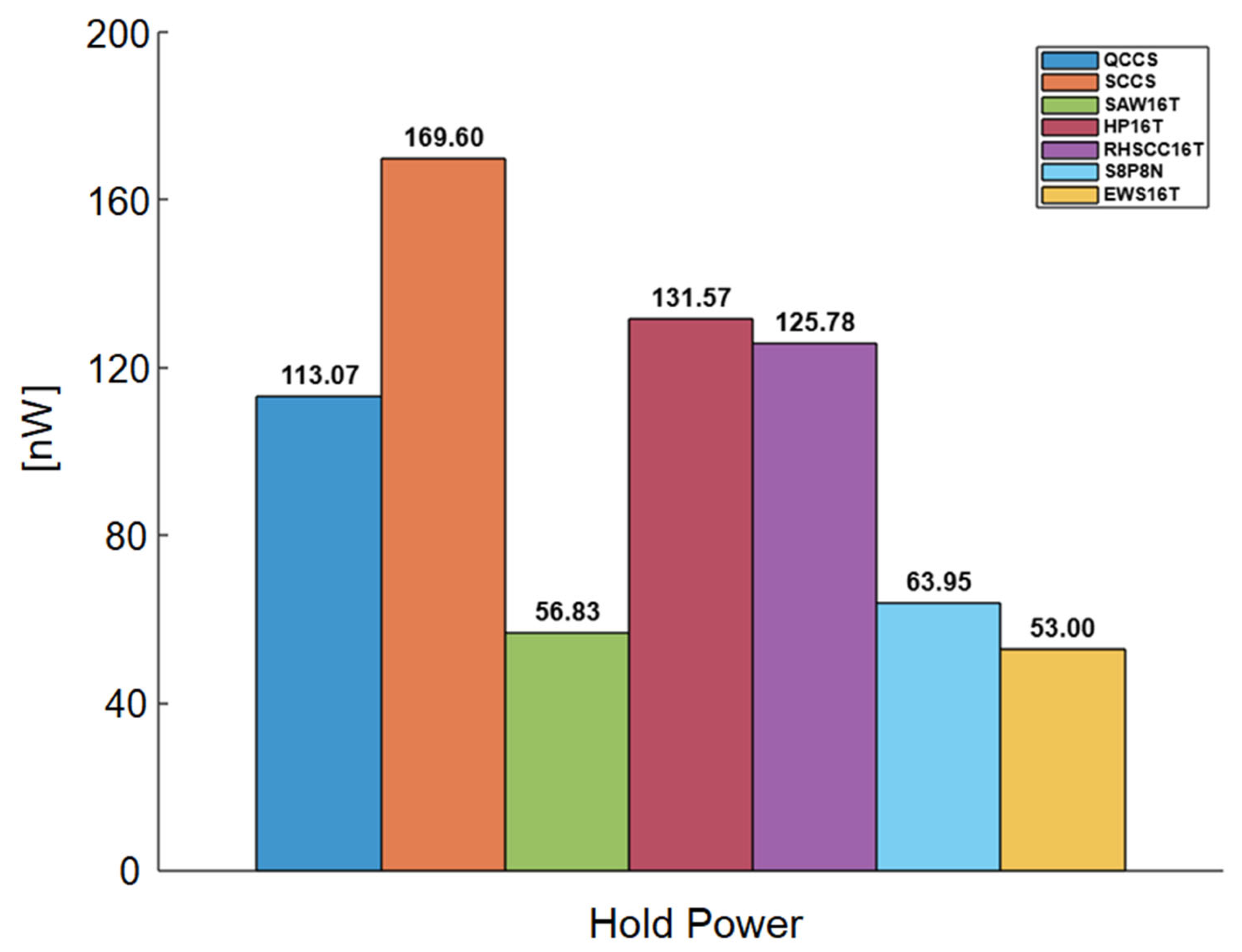
Figure 11 present the bar graphs in the order of QCCS, SCCS, SAW16T, HP16T, RHSCC16T, S8P8N, and EWS16T from left to right.
3.1. Write Delay Comparison
Write delay, also referred to as write access time (WAT), is defined as the time interval between the moment the word line voltage reaches 50% of its full swing and the point at which the storage nodes Q and QB intersect [
15].
Figure 6 compares the WAT of various SRAM cells, including QCCS, SCCS, SAW16T, HP16T, RHSCC16T, S8P8N, and the proposed EWS-16T cell. As illustrated in the figure, the EWS-16T cell exhibits the shortest write delay among all the evaluated designs, demonstrating superior performance in write operations.
The proposed EWS-16T employs a dual-access transistor structure composed of both PMOS and NMOS transistors, enabling simultaneous and fast control of the storage nodes (Q, QB) and the internal nodes (S0, S1). This bidirectional conduction structure facilitates rapid voltage inversion during write operations, effectively reducing the WAT. Furthermore, the cell is initialized with a weak ‘1’ at the storage node and a weak ‘0’ at the internal node, allowing reliable switching with minimal charge disturbance. In addition, the PMOS pull-up transistors connected to the storage node are sized to be 1.7× wider than the access transistor, making the storage node weaker and thus allowing the access transistor to discharge the ‘1’-storing node more effectively. According to experimental results, the proposed EWS-16T achieves a WAT of 22.11 ps, which is 1.89×, 1.95×, 1.54×, 2.17×, 1.69×, and 1.29× faster than QCCS, SCCS, SAW16T, HP16T, RHSCC16T, and S8P8N cells, respectively.
3.2. Write Capability Comparison
WWTV is defined as the word line voltage at which the storage nodes Q and QB intersect during a write operation. This dynamic metric reflects a cell’s writability and internal drive strength under realistic conditions. Unlike static measures such as Static Noise Margin (SNM), WWTV offers a more accurate indication of write capability, especially in high-speed and low-voltage environments [
16].
Figure 7 compares the WWTV of various SRAM designs, including QCCS, SCCS, SAW16T, HP16T, RHSCC16T, S8P8N, and the proposed EWS-16T cell. Higher WWTV indicates stronger internal node controllability, enabling more reliable and efficient writes. As shown, cells with longer write access times generally show lower WWTV, while those with faster write access times achieve higher WWTV, confirming the correlation between write speed and dynamic writability. The proposed EWS-16T, with its dual-access structure and optimized PMOS pull-up ratio, achieves the highest WWTV while also exhibiting the shortest WAT among all comparison cells. These features highlight its excellent internal drivability and write efficiency under dynamic conditions. However, this enhancement in writability achieved by upsizing access and pull-up transistors to increase WWTV also weakens the storage node, making it more susceptible to voltage disturbance during reads and thus reducing RSNM. This trade-off arises because stronger write paths lower the voltage margin necessary for stable read sensing. To address this, careful transistor sizing and selective feedback control are required to improve RSNM without significantly compromising write performance. Experimental results show that EWS-16T achieves a WWTV of 279 mV, which is 3.40×, 4.04×, 1.76×, 1.11×, 2.20×, and 1.30× higher than QCCS, SCCS, SAW16T, HP16T, RHSCC16T, and S8P8N, respectively. These results confirm its superior dynamic write stability and robustness for SRAM applications.
3.3. Read Delay Comparison
Read delay, also referred to as read access time (RAT), is defined as the time interval from when the WL voltage reaches 50% of VDD to the moment a voltage difference of 50 mV is established between the BL and the complementary BLB [
15]. This metric is significantly influenced by the read current through the access and pull-down transistors, as well as the capacitance associated with the bitlines. The proposed EWS-16T cell includes two pairs of access transistors; however, only one pair is utilized during read operations to connect the storage nodes to the bitlines. The remaining pair remains inactive and introduces parasitic capacitance, which degrades the read current path and increases the overall read delay. Additionally, the internal feedback structure, which is optimized for soft-error resilience and write performance, adds resistance and capacitance to the read path, further impacting read speed.
As illustrated in
Figure 8, the EWS-16T cell exhibits a longer read delay compared to other reference cells, including QCCS, SCCS, SAW16T, HP16T, RHSCC16T, and S8P8N. This reflects a structural trade-off, where enhancements in write performance are achieved at the expense of read delay due to parasitic and feedback-related effects during the read operation.
3.4. Read Capability Comparison
Read stability refers to the ability of an SRAM cell to preserve the stored value at a storage node during a read operation, without being disturbed by noise or internal coupling. It is typically evaluated using the RSNM, which is measured by precharging both BL and BLB to VDD and extracting the voltage transfer characteristics through the butterfly curve method. A higher RSNM indicates stronger noise immunity and better read stability [
17]. During read operations, the proposed EWS-16T cell utilizes only one pair of access transistors to connect the storage nodes to the bitlines, while the remaining pair remains electrically present but inactive. These unused transistors introduce parasitic coupling between the storage and internal nodes, acting as additional load elements that weaken voltage stability. Furthermore, the feedback structure between the storage and internal nodes, although beneficial for soft-error resilience, increases the susceptibility of the cell to noise during read access, thereby reducing RSNM.
As shown in
Figure 9, the EWS-16T cell exhibits a lower RSNM than other comparison cells such as QCCS, SCCS, SAW16T, HP16T, RHSCC16T, and S8P8N. This indicates that while the proposed design delivers strong write performance through its dual-access structure and optimized pull-up ratio, its read stability is comparatively limited due to the added complexity of its internal node structure and feedback paths. To enhance RSNM, read-assist techniques such as negative bitline (NBL) or boosted word line can be employed to increase the voltage differential between bitlines during read operations [
18,
19]. In addition, layout optimization and careful transistor sizing can help achieve a balanced trade-off between read stability and write efficiency.
3.5. Hold Capability Comparison
The HSNM represents the ability of an SRAM cell to retain data reliably when all access transistors are turned off and the BL and BLB are precharged. It serves as a key indicator of voltage stability during hold mode. To improve radiation hardness, the proposed EWS-16T cell incorporates a complex node configuration that includes both storage nodes (Q, QB) and internal nodes (S0, S1). However, this increased complexity also introduces stronger inter-node coupling, which can slightly degrade the voltage stability of the storage nodes during hold conditions. In general, radiation-hardened SRAM cells must balance competing design requirements. Enhancing soft-error resilience often comes at the cost of larger cell area, higher power consumption, increased circuit complexity, and a reduction in HSNM. As illustrated in
Figure 10, the EWS-16T cell shows a lower HSNM than other hardened designs such as QCCS, SCCS, SAW16T, HP16T, RHSCC16T, and S8P8N. This reflects a conscious design trade-off that prioritizes soft-error tolerance and operational robustness in radiation-intensive environments, even at the expense of some hold stability.
3.6. Hold Power Comparison
In SRAM cells, the hold mode is defined as the state in which the WL is deactivated and both BL and BLB are precharged to a high voltage level. During this mode, the proposed EWS-16T cell minimizes leakage paths by completely isolating the storage nodes from the bitlines—achieved by turning off both the access transistors (N7/N8) and the additional PMOS transistors (P7/P8). Moreover, the cross-coupled structure adopted in the EWS-16T enhances storage node stability and effectively suppresses loop-induced leakage current. Additionally, the storage nodes retain weak logic levels (‘1’ at Q and ‘0’ at S0), which helps reduce the voltage difference across internal nodes, thereby further minimizing leakage.
As shown in
Figure 11, the EWS-16T cell achieves a hold power of 53 nW, which is 2.13×, 3.20×, 1.07×, 2.48×, 2.37×, and 1.20× lower than those of QCCS, SCCS, SAW16T, HP16T, RHSCC16T, and S8P8N, respectively. These results confirm that the EWS-16T cell outperforms conventional radiation-hardened SRAM designs in terms of power efficiency during idle states. Through these structural and electrical optimizations, it can be concluded that the EWS-16T cell effectively suppresses leakage current even in hold mode, achieving significantly improved low-power operation suitable for space applications.
3.7. Soft Error Robustness Verification and Comparison
To evaluate the soft-error resilience of the proposed EWS-16T cell, a double-exponential current model was employed to simulate SEUs. The injected transient current I(t) is described by the following equation [
7].
Here,
is approximated from the total deposited charge
Q using the following equation.
In this model,
Q denotes the total deposited charge. The parameters
and
represent the junction collection time constant (200 ps) and the ion track establishment time constant (50 ps), respectively. Experimental results show that when 300 fC of charge is individually injected into sensitive nodes
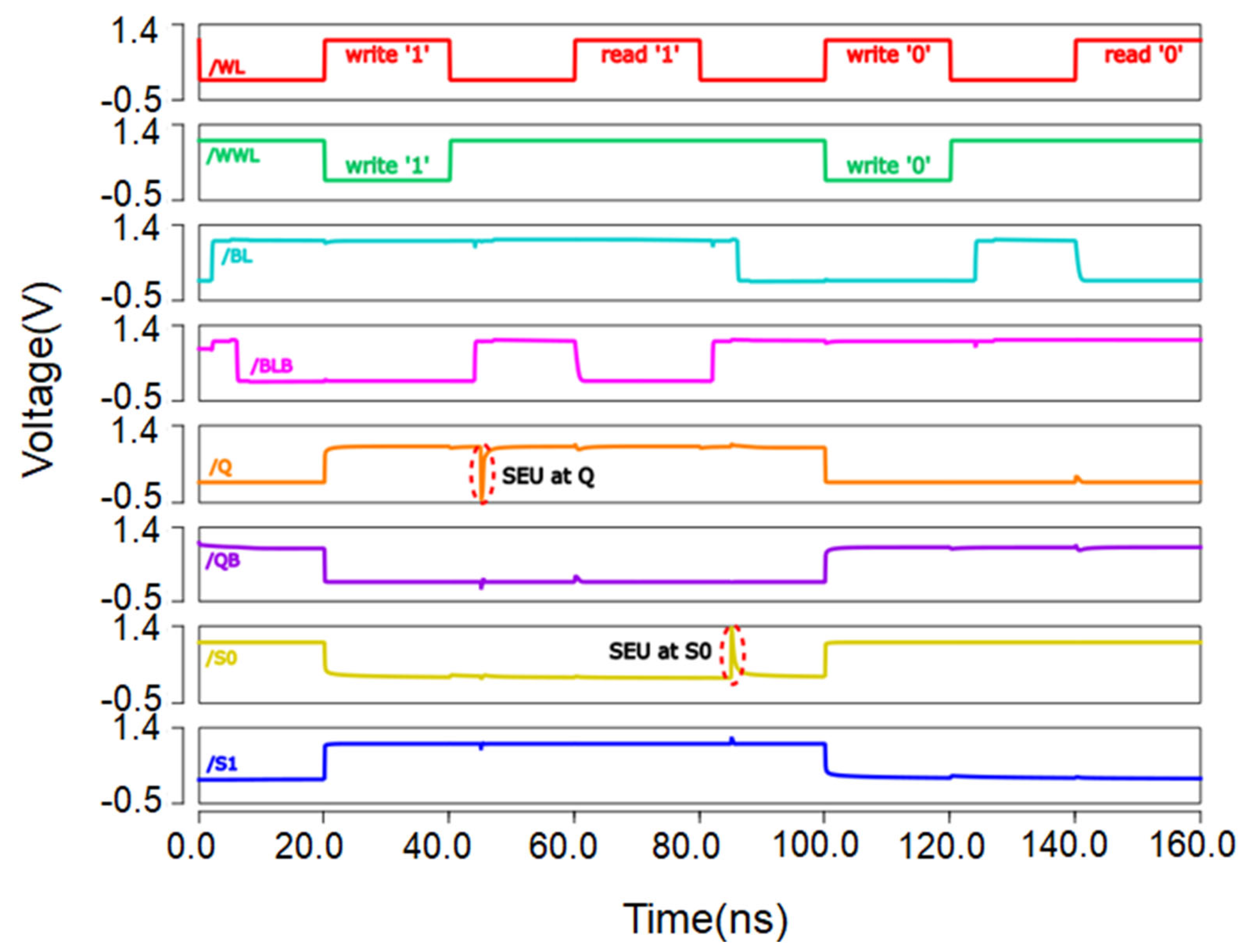
Q and S0, the proposed EWS-16T cell successfully restores its original state in both cases, demonstrating excellent tolerance to SEUs.
Figure 12 shows the SEU scenarios for nodes
Q and S0, respectively, where the node voltages recover to their original stable levels over time.
To further evaluate multi-node soft-error resilience, charge was simultaneously injected into pairs of sensitive nodes. The EWS-16T cell successfully recovered in all combinations except when both Q and S0 were struck simultaneously. In this case, simultaneous disturbance of the internal feedback loop prevented recovery. However, the proposed cell addresses this limitation through a layout that ensures sufficient spacing between sensitive transistors, thereby suppressing charge-sharing-induced simultaneous inversions.
3.8. Electrical Quality Metric
The critical charge (Qc) is an important metric for evaluating the soft-error tolerance of SRAM cells. However, the overall performance of SRAM cells is determined not only by Qc but also by various other parameters such as RAT, WAT, WWTV, RSNM, HSNM, and hold power. In this work, an overall evaluation of SRAM cell performance is conducted by calculating the EQM, which comprehensively considers these major design parameters [
20]. The EQM is defined as follows.
A higher EQM value indicates superior overall performance of the SRAM cell. The EQM values of all designs were directly compared using the absolute scores obtained from the defined performance equation, without normalization. Experimental results show that the proposed EWS-16T cell achieves the highest EQM among all evaluated designs, demonstrating excellent overall performance in terms of write characteristics, soft-error resilience, and power efficiency.
Table 1 summarizes the key performance parameters used for EQM calculation, including Qc, RAT, WAT, WWTV, RSNM, HSNM, and hold power, for all compared SRAM cells.
Figure 13a presents the comparison of EQM values for all cells. Additionally,
Figure 13b shows the comparison of weighted EQM values, where the EWS-16T cell demonstrates superior performance compared to the other cells in both cases. To reflect application-specific priorities, a sensitivity analysis was performed by applying a weight factor of 1.1 to Qc and 0.9 to hold power.
Figure 13b presents the resulting EQM values based on this weighted configuration. These two parameters are particularly important in space exploration and low-power applications. Even with the applied weights, the EWS-16T cell maintained the highest EQM, demonstrating robust performance under varied design conditions.
4. Conclusions
In this study, a 16-transistor radiation-hardened SRAM cell, named EWS-16T, was proposed to address soft-error issues in space environments. Through comprehensive simulations using a double-exponential current injection model, the cell demonstrated robust self-recovery capabilities when 300 fC of transient charge was individually injected into each sensitive node. This confirms the cell’s strong resilience against SEUs. Furthermore, in SEMNU scenarios, the cell successfully recovered in all tested node pair combinations except when both Q and S0 were simultaneously struck. This critical case is effectively mitigated at the layout level by ensuring sufficient physical spacing between sensitive nodes, reducing the likelihood of charge-sharing-induced simultaneous upsets. Given its strong resilience to SEUs and SEMNUs, along with low power consumption, the proposed EWS-16T cell is well-suited for deployment in radiation-critical space applications. It can be effectively utilized in on-board memories of CubeSats, deep-space exploration systems, and embedded caches in launch vehicle controllers, where both energy efficiency and fault tolerance are essential.
The proposed EWS-16T cell achieved a critical charge exceeding 300 fC, significantly higher than that of conventional hardened cells such as QCCS, SCCS, and RHSCC16T, demonstrating superior radiation tolerance. In addition, it exhibited the shortest write access time and the highest WWTV among all comparison cells. It also achieved the lowest hold power consumption, indicating excellent energy efficiency. However, due to its dual-access structure and complex internal feedback paths, the cell showed relatively lower performance in terms of read delay, RSNM, and HSNM.
Despite these limitations, the EQM evaluation revealed that the EWS-16T cell achieves the highest overall performance among all evaluated designs. This is attributed to its optimized transistor sizing, enhanced feedback architecture, and reduced static power consumption, resulting in a well-balanced trade-off between write efficiency, soft-error resilience, and power performance. To further reinforce these results, future studies will include physical verification, extended charge injection experiments beyond 300 fC, and detailed Monte Carlo simulations to validate the cell’s performance under practical operating conditions.
The proposed EWS-16T cell is expected to be scalable to advanced technology nodes such as 28 nm CMOS and FD-SOI. These nodes offer advantages such as lower junction capacitance and improved radiation tolerance. In addition, the flexible layout and transistor sizing of the EWS-16T allow effective adaptation to increased variability and leakage current in nanoscale technologies. As a result, the cell can maintain stable operation even under advanced process conditions.
In conclusion, the proposed EWS-16T cell offers a highly promising solution for radiation-hardened SRAM applications in space and other extreme environments, combining strong soft-error recovery, low power consumption, and enhanced write capability into a reliable and efficient memory design. Moreover, the proposed cell can be used together with ECC techniques to further enhance system reliability, and it functions not as a replacement for ECC but as a complementary approach. Therefore, the proposed EWS-16T cell is highly suitable for integration into compact platforms such as CubeSats and nanosatellites, where both high integration density and robust radiation tolerance are essential requirements.
Author Contributions
Conceptualization, S.-J.K. and S.-H.J.; methodology, S.-J.K.; validation, S.-J.K.; data curation, S.-J.K.; writing—original draft preparation, S.-J.K.; writing—review and editing, S.-H.J.; visualization, S.-J.K.; supervision, S.-H.J.; project administration, S.-H.J. All authors have read and agreed to the published version of the manuscript.
Funding
This research received no external funding.
Institutional Review Board Statement
Not applicable.
Informed Consent Statement
Not applicable.
Data Availability Statement
Data are contained within the article.
Acknowledgments
The EDA tool was supported by the IC Design Education Center, Korea.
Conflicts of Interest
The authors declare no conflicts of interest.
References
- Pal, S.; Sri, D.D.; Ki, W.-H.; Islam, A. Soft-Error Resilient Read Decoupled SRAM with Multi-Node Upset Recovery for Space Applications. IEEE Trans. Electron Devices 2021, 68, 2246–2254. [Google Scholar] [CrossRef]
- Mukku, P.K.; Lorenzo, R. A Soft Error Upset Hardened 12T-SRAM Cell for Space and Terrestrial Applications. Mem.-Mater. Devices Circuits Syst. 2023, 6, 100092. [Google Scholar] [CrossRef]
- Jahinuzzaman, S.M.; Rennie, D.J.; Sachdev, M. A Soft Error Tolerant 10T SRAM Bit-Cell with Differential Read Capability. IEEE Trans. Nucl. Sci. 2009, 56, 3768–3773. [Google Scholar] [CrossRef]
- Xiong, Y.; Pieper, N.J.; Kronenberg, J.B.; Delaney, M.; Sanchez, C.N.; Ball, D.R.; Casey, M.; Fung, R.; Wen, S.-J.; Bhuva, B.L. SEU Cross-Section Trends for Threshold Voltage Options from 16-Nm to 3-Nm Bulk FinFET Nodes. IEEE Trans. Nucl. Sci. 2024, 72, 1479–1485. [Google Scholar] [CrossRef]
- Dohar, S.S.; Siddharth, R.K.; Vasantha, M.H.; YB, N.K. A 1.2 V Single Event Multinode Upset Tolerant RHSC 12T Memory Cell in 65-Nm CMOS. IEEE Trans. Electron Devices 2023, 71, 1054–1059. [Google Scholar] [CrossRef]
- Bajura, M.A.; Boulghassoul, Y.; Naseer, R.; DasGupta, S.; Witulski, A.F.; Sondeen, J.; Stansberry, S.D.; Draper, J.; Massengill, L.W.; Damoulakis, J.N. Models and Algorithmic Limits for an ECC-Based Approach to Hardening Sub-100-Nm SRAMs. IEEE Trans. Nucl. Sci. 2007, 54, 935–945. [Google Scholar] [CrossRef]
- Li, P.; Wang, X.; Zhang, Y.; Wang, H.; Lu, J.; Zhao, Q.; Hao, L.; Peng, C.; Lu, W.; Lin, Z. Novel Radiation-Hardened-by-Design (RHBD) 14T Memory Cell for Aerospace Applications in 65 Nm CMOS Technology. Microelectron. J. 2023, 141, 105954. [Google Scholar] [CrossRef]
- Yan, A.; Xiang, J.; Cao, A.; He, Z.; Cui, J.; Ni, T.; Huang, Z.; Wen, X.; Girard, P. Quadruple and Sextuple Cross-Coupled SRAM Cell Designs with Optimized Overhead for Reliable Applications. IEEE Trans. Device Mater. Reliab. 2022, 22, 282–295. [Google Scholar] [CrossRef]
- Bai, N.; Zhao, W.; Xu, Y.; Wang, Y. A Low-Energy Critical Charge-Enhanced SRAM for Aerospace Applications. In Proceedings of the 2024 IEEE International Test Conference in Asia (ITC-Asia), Changsha, China, 18–20 August 2024; IEEE: New York, NY, USA, 2024; pp. 1–6. [Google Scholar]
- Kumar, S.; Mukherjee, A. High Performance Radiation-Hardened SRAM Cell Design for Robust Applications. Microelectron. J. 2023, 140, 105934. [Google Scholar] [CrossRef]
- Bharti, P.K.; Mekie, J. RHSCC-16T: Radiation Hardened Sextuple Cross Coupled Robust SRAM Design for Radiation Prone Environments. In Proceedings of the 2022 IEEE 40th International Conference on Computer Design (ICCD), Olympic Valley, CA, USA, 23–26 October 2022; IEEE: New York, NY, USA, 2022; pp. 17–24. [Google Scholar]
- Bai, N.; Xiao, X.; Xu, Y.; Wang, Y.; Wang, L.; Zhou, X. Soft-Error-Aware Sram with Multinode Upset Tolerance for Aerospace Applications. IEEE Trans. Very Large Scale Integr. (VLSI) Syst. 2023, 32, 128–136. [Google Scholar] [CrossRef]
- Guo, J.; Xiao, L.; Mao, Z. Novel Low-Power and Highly Reliable Radiation Hardened Memory Cell for 65 Nm CMOS Technology. IEEE Trans. Circuits Syst. I Regul. Pap. 2014, 61, 1994–2001. [Google Scholar] [CrossRef]
- Radamson, H.H.; Zhu, H.; Wu, Z.; He, X.; Lin, H.; Liu, J.; Xiang, J.; Kong, Z.; Xiong, W.; Li, J. State of the Art and Future Perspectives in Advanced CMOS Technology. Nanomaterials 2020, 10, 1555. [Google Scholar] [CrossRef] [PubMed]
- Pal, S.; Ki, W.-H.; Tsui, C.-Y. Soft-Error-Aware Read-Stability-Enhanced Low-Power 12T SRAM with Multi-Node Upset Recoverability for Aerospace Applications. IEEE Trans. Circuits Syst. I Regul. Pap. 2022, 69, 1560–1570. [Google Scholar] [CrossRef]
- Cheng, X.; Hu, Y.; Miao, T.; Liu, W.; Zheng, Q.; Liu, Y.; Liang, J.; Chen, L.; Guo, A.; Yin, L.; et al. A Novel Design for SRAM Bitcell with 3-Complementary-FETs. arXiv 2025, arXiv:2503.06448. [Google Scholar] [CrossRef]
- Singh, P.; Vishvakarma, S.K. Ultra-Low Power, Process-Tolerant 10T (PT10T) SRAM with Improved Read/Write Ability for Internet of Things (IoT) Applications. J. Low Power Electron. Appl. 2017, 7, 24. [Google Scholar] [CrossRef]
- Peng, C.; Chen, Z.; Zhang, J.; Xiao, S.; Liu, C.; Wu, X.; Lin, Z. A Radiation Harden Enhanced Quatro (RHEQ) SRAM Cell. IEICE Electron. Express 2017, 14, 20170784. [Google Scholar] [CrossRef][Green Version]
- Zimmer, B.; Toh, S.O.; Vo, H.; Lee, Y.; Thomas, O.; Asanovic, K.; Nikolic, B. SRAM Assist Techniques for Operation in a Wide Voltage Range in 28-Nm CMOS. IEEE Trans. Circuits Syst. II Express Briefs 2013, 59, 853–857. [Google Scholar] [CrossRef]
- Oh, J.-Y.; Jo, S.-H. Radiation-Hardened 16T SRAM Cell with Improved Read and Write Stability for Space Applications. Appl. Sci. 2024, 14, 11940. [Google Scholar] [CrossRef]
| Disclaimer/Publisher’s Note: The statements, opinions and data contained in all publications are solely those of the individual author(s) and contributor(s) and not of MDPI and/or the editor(s). MDPI and/or the editor(s) disclaim responsibility for any injury to people or property resulting from any ideas, methods, instructions or products referred to in the content. |
© 2025 by the authors. Licensee MDPI, Basel, Switzerland. This article is an open access article distributed under the terms and conditions of the Creative Commons Attribution (CC BY) license (https://creativecommons.org/licenses/by/4.0/).

