Abstract
The performance of long-wave infrared (LWIR) quantum well (QWIP) detection systems is seriously affected by the dark current of the detectors. Tiny variations in the focal-plane temperature of the devices cause fluctuations in the dark current, which in turn generate temporal noise. It is difficult to measure the dark current accurately after the detector assembly is packaged. To address the above problems, a QWIP dark current measurement method based on focal-plane temperature is proposed, as well as a method to reduce dark current noise. First, the response model of the LWIR QWIP detection system was established, and the dark current model was introduced. Then, the detection system components were introduced, chiller calibration experiments were carried out, and the dark current values of the QWIP at different temperatures were measured by combining the system design and parameters. Next, the dark current noise correction method was proposed, the target data were collected, and experiments were carried out to correct them. Finally, after the calculation, the temporal noise was reduced by 57.69% after the correction, which is proof of a significant effect. This method can obtain the real-time dark current value by collecting the focal-plane temperature data, and reduce the dark current temporal noise (difficult to eliminate using conventional methods), which is beneficial for promoting the application of QWIPs in LWIR remote sensing detection.
1. Introduction
The detector is the heart of an infrared detection system. The third-generation infrared photodetector SWaP3 (Size, Weight, Power, Performance and Price) concept is centered on improving performance with a smaller size, lower weight, lower power consumption, and cheaper cost [1]. For detectors in different spectral ranges, their own temperature affects them differently. The mainstream cooled LWIR (8~12 μm) detectors of SWaP3 are HgCdTe (cadmium mercury telluride), QWIP, and T2SL (type ii superlattice) [2,3,4]. These types all require liquid nitrogen and need to be below the target cooling temperature to achieve good sensitivity in engineering applications. The body temperature of infrared cameras for satellite-borne Earth observation is close to the temperature of the detection target, and the detection effect is drastically affected by its own thermal radiation [5]. When working in orbit for a long time, the load’s hood, external mechanism materials, and surface coatings show different degrees of degradation, which can cause the cooler to work in a poorer thermal environment [6,7]. Whether it is the geostationary satellite FY-4 or the sun-synchronous orbit satellites HJ-2 and the Gaofen-4 satellite, there are fluctuations of about ten degrees outside the detector cooler [8,9,10,11]. Factors such as the thermal environment and the performance of the cooler itself generate irregular fluctuations in the focal-plane temperature, and the dark current and its voltage signal obtained through integration vary with temperature, while bringing low-frequency time noise [8].
The QWIP has been widely used in recent years in LWIR detection systems, such as QWEST, Landsat 8 TRIS 1, and Landsat 9 TRIS 2 [12,13,14]. The materials typically used in QWIP devices are GaAs/AlGaAs [2]. The detector works as follows: the constituent materials form electron and hole potential wells in the energy band structure; photons from various sources cause the material to also produce electron and hole jumps for interband jumps in the sub-band; and an electric field is introduced externally to produce carriers, which are obtained through the electrodes and converted into a photocurrent. QWIPs have the following advantages: the GaAs substrate process is mature and has good lattice matching, which can support the preparation of large-area quantum well materials, while also having good uniformity, solid pixel material, and strong radiation resistance; it is also easy to change the device response band. Covering a wide spectral range, the system-related technology can be extended to other bands of detection; materials are easy to splice, with a high yield rate. For engineering applications, the target cooling temperature is typically 40~50 K for QWIP and around 77 K for HgCdTe. The dark current of QWIP is lower than that of HgCdTe at the respective typical cooling temperatures. The production difficulty of large-array HgCdTe detectors is high, and a QWIP is more likely to be the device of choice for projects with large-detector-volume requirements. At the same time, QWIPs have the disadvantage that the quantum efficiency at suitable operating points is one order of magnitude lower than that of HgCdTe [15]. The target cooling temperature is low, generally below the temperature of liquid nitrogen; additionally, according to Fourier’s law, the larger the temperature difference between the inside and outside of the dewar, the higher the heat flux, which challenges the temperature control level of the detector assembly, where very small temperature fluctuations may lead to changes in the focal-plane dark current.
The dark current in a quantum well structure is mainly composed of free electrons drifting above the potential barrier and electrons captured by and emitted from the quantum well [15]. Levine, Kane, and Liu systematically investigated the dark current mechanism in a QWIP and developed an analytical model [15,16,17]. The models have the following assumptions: the dominant component of the dark current is the thermal excitation current, the proportion of the continuous tunneling current to the dark current can be neglected, and both the light and electric field distributions are ideally homogeneous. All three models were experimentally verified to be reasonable. There were some problems in the application of the analytic model, such as errors in calculating the dark current of the same focal-plane device in different states. There are numerous parameters in the equation for calculating the dark current in the Levine model, including the electric field strength, electron drift velocity, and thermal excitation energy, which are difficult to measure accurately at the same time.
Dark current is the main parameter governing the performance of a QWIP detection system. It is important to monitor the dark current and its generated response in real-time. After integrating the whole satellite-borne on-board IR detection system until the on-orbit operation, the focal-plane dark current value is difficult to measure accurately in real-time. Both Landsat 8 TRIS and this research team set up dark pixels at the QWIP, and the response of the dark pixels can be used as a reference for the overall dark current level of the device [18,19]. A recurrent neural network was used to obtain the relationship between the dark pixels and the imaging pixels, which was then corrected for the target data. The above method cannot be applied to QWIP detection systems without dark pixels. Using semiconductor simulation software such as Sentaurus TCAD, the QWIP structure characteristics determined that the dark current simulation was difficult to conduct below the temperature of liquid nitrogen. The method of dark current noise suppression with a readout circuit is highly accurate, but the presence of this circuit increases the overall detector size and power consumption, complicates the fabrication process, and is not validated at a low cooling temperature or in large surface array detectors [20]. Multiple radiometric calibrations in a short period can reduce the effect of dark current noise, but this compresses the continuous imaging time, especially in hyperspectral detection, and misses part of the focused spatial dimensional image information [21].
In this study, the signal full-link response model of the satellite-borne LWIR QWIP detection system is established, and the QWIP dark current model is elaborated as the theoretical basis of the method. A method of measuring dark current based on focal-plane temperature data and a correction method of dark current temporal noise are introduced. The structure of the detection system and the design details closely related to this method are described in the experimental section, experimental verification is carried out and results are obtained, and the experimental steps and conclusions are analyzed.
2. Dark Current Measurement and Noise Correction Method Based on Focal-Plane Temperature
The main structure schematic of this paper is shown in Figure 1. Firstly, the response model and dark current model of the LWIR QWIP detection system are introduced. Then, the dark current measurement method is highlighted, and a dark current noise correction method is proposed. Then, the components of each module of the satellite-borne LWIR QWIP detection system used in the study are introduced. Finally, the experimental part is presented.
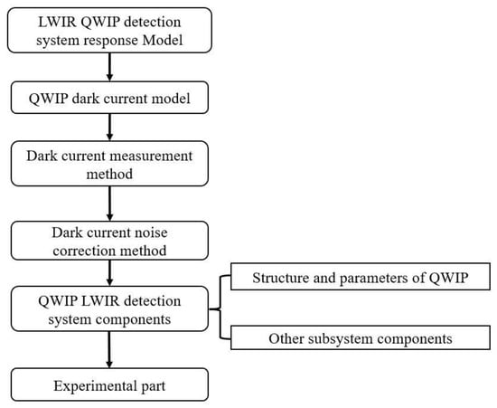
Figure 1.
Schematic diagram of dark current measurement and noise correction method.
2.1. LWIR QWIP Detection System Response Model
The response model of the detection system is analyzed in this section in order to clearly demonstrate the effect of dark currents and their noise on the system. The total detector response voltage consists of the response voltages of the target object radiation, internal background radiation of the dewar, background radiation of the optical system and dark current, and the bias voltages of the readout and information acquisition circuits [22].
where is the total detector response voltage, is the response voltage of the target object, is the response voltage of the background light inside the dewar, is the response voltage of the optical system background, is the dark current response voltage, and is the bias voltage of the readout circuit and the information acquisition circuit. It is shown in the study that the focal-plane operates below the temperature of liquid nitrogen (the QWIP cooling target temperature range for engineering applications) and the photocurrent does not change with the temperature of the focal-plane when facing the same target object. Therefore, with the detection target, acquisition environment, and operating mode unchanged, only the dark current response voltage change can cause a change in the total detector response voltage . The dark current response voltage is expressed as:
where is the integration time, is the integration capacitance, and is the dark current magnitude.
Figure 2 visualizes the response mode of the LWIR QWIP hyperspectral detection system. This detection system works on an Earth-orbiting satellite and periodically detects certain locations on Earth. The light from the target object passes through the main optics, the beam splitting system, the detector’s window, and the pixels in sequence. The radiation of the target in the same spatial dimension is spectroscopically divided by the hyperspectrometer. The value of radiation after spectroscopy is only 1% of that of the gaze-type detection system [23]. Therefore, the amount of target object radiation and incident photons received by the detector pixels is very small, while the effect of the spectrometer background radiation and the detector dark current is relatively greater.
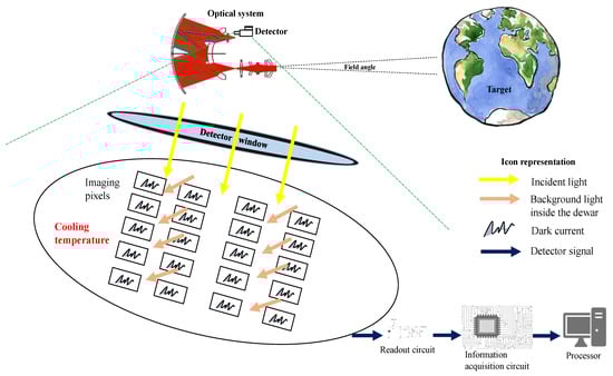
Figure 2.
LWIR QWIP detection system response model.
2.2. QWIP Dark Current Model
The dark current of the QWIP device can be expressed as:
where is the number of electrons of the dark current transmitted continuously in the thermally excited state, is the electronic charge, is the transmission velocity, and is the area of the photosensitive pixel.
The number of electrons in the dark current can be expressed as [17]:
where is the effective mass of the electron, is the Planck constant, is the quantum well period number, is the ground state energy, is the Fermi factor, V is the bias voltage of the QWIP, and is the individual barrier current transport factor. When the thermal excitation effect is dominant in the dark current, = 1; when the phonon-assisted attempted penetration effect is dominant, = 0. The expression of the Fermi factor is:
where is the Fermi energy level, is the focal-plane temperature, and is the Boltzmann constant.
From Equations (3)–(5), it can be concluded that the magnitude of the dark current is directly related to the temperature and the bias voltage , which are the most easily adjustable operating conditions after the detector is packaged. Under ordinary bias (0~3 V), the thermal excitation effect is discussed as the dark current dominant mechanism by adding the condition (E > ) to Equation (4), where is the energy required for the leap. Equation (4) can be simplified to Equation (6):
where and are the conduction band and valence band energies. The conduction band is the difference between the spectral cutoff energy and the ground state energy:
Important dark current versus temperature relationships were obtained for:
The above is the dark current divided by the temperature, with e as the exponential function of the base and temperature as the variable, and the two are proportional to each other. The energy between the conduction band and valence band of the same QWIP device is fixed, so is constant. There are sufficient experiments to prove the correctness of Equation (8)’s conclusion in Levine’s study, wherein two QWIP devices with different spectral detection ranges were prepared, the dark currents were measured by changing several temperature points (ranging from 25 K to 120 K), and the relationship between dark currents and temperature was obtained. The theoretical model of Equation (8) plays an important role in this study and is described in detail in the subsequent sections.
2.3. Dark Current Measurement Method
This study applies a sub-band continuum leap type (B-C) QWIP with a large spectral bandwidth and a slightly higher dark current compared to other types of QWIP [24]. The operating principle of the temperature measurement diode is to use the characteristic of the forward voltage drop with temperature when the diode PN junction is under the action of a constant-current source for temperature measurement. In the operating range, the forward voltage drop has a good linear relationship with temperature. However, there is a certain bias in the constant-current source and temperature measurement diode circuit, and to accurately obtain the relationship between the temperature measurement pin output voltage and the temperature of a certain QWIP device, a test calibration is required. The chiller calibration equation is as follows:
where is the voltage value of the temperature measurement pin, is the cooling target temperature, and and are the linear parameter and intercept of the relationship, respectively. By adjusting multiple , is measured at different temperatures.
The signal is preprocessed in the information acquisition circuit by an op-amp for linear operations. The above preprocessing can make the best possible use of the sampling range of the analog-to-digital converter (ADC) and improve the signal-to-noise ratio of the temperature measurement signal. The preprocessed temperature measurement voltage is
where is the subtractive circuit deduction voltage and is the amplification.
The temperature measurement quantization value is obtained by calculating:
where is the lower limit of the input voltage interval of the ADC of the temperature measurement module, is the input voltage range, and is the number of quantization bits.
Equation (8) is the relationship between dark current and temperature [17]. The dark current of the QWIP is easily and accurately measured using a fully enclosed cold screen and dedicated measurement equipment during the device preparation stage and before the fixed package is performed. In the temperature region where the thermal excitation effect is the dominant mechanism of the dark current, there is an exponential relationship between the dark current and temperature. Taking the logarithm of both sides of the equation of Equation (8) with a base of 10, the equation is obtained as:
Consider the left side of the equation as the dependent variable, where , are the linear parameters and intercepts of the linear relationship of Equation (9), respectively. The two sets of and are obtained to solve for , of the same QWIP device.
In summary, the QWIP dark current values of the same QWIP device at any temperature under the thermal excitation effect as the dark current dominant mechanism can be measured by combining Equations (9)–(12).
2.4. Dark Current Noise Correction Method
After the analysis in the previous section, the overall dark current of the QWIP focal-plane changes due to temperature fluctuations, which in turn causes changes in the pixel response and generates low-frequency time noise. The introduction of a method to eliminate this type of dark current time noise forms the main content of this section.
Focal-plane devices usually set a target cooling temperature, . is essentially the same physical quantity as the previously mentioned T. is used for experiments and T is used for theoretical analysis. The performance of the refrigeration machine varies, and the rated operating mode of generates temperature fluctuations of . After obtaining the parameters of Equation (12), this equation can be used to solve for the dark current value at multiple temperature points in the range of . Within a very small temperature difference , a good linear relationship exists between and temperature. The quantized values of temperature measurement, corresponding to and , , and , can be obtained with Equations (9)–(11). Then, both temperature and response are transformed into the form of response values, and the linear relationship between the two is solved to obtain the change in response values under equal temperature changes.
The design of the information acquisition circuit includes a module for the preprocessing and quantization of the detector signal. The preprocessed detector signal voltage is:
where is the preprocessed detector signal voltage, is the bias subtraction voltage of the preprocessing circuit, and is the gain of the preprocessing circuit.
The quantized response value of the detector signal is:
where is the quantized detector response value, is the lower limit of the input voltage interval of the ADC of the preprocessing module, is the input voltage range, and is the number of quantization bits.
The detector signal quantization value corresponding to can be obtained according to Equations (13) and (14).
The coefficient of the system response value with respect to the temperature response value is obtained by solving:
The corrected system response value is:
where is the mean value of the response of the temperature measurement pin during the time of data acquisition. Since the dark current variation occurs within the pixels, independent of the spectroscopic system, the method can be applied to QWIP hyperspectral imagers and gaze-type cameras for the indistinguishable correction of the pixels for each spectral channel or face array spatial dimension.
The direct use of temperature measurement pin response data for target data correction, without a corresponding theoretical basis, is a purely mathematical method. The present method incorporates a physical model with reliable theoretical support.
3. Dark Current Measurement Based on Focal-Plane Temperature and Dark Current Correction Experiment
3.1. Satellite-Borne LWIR QWIP Detection System
The LWIR QWIP detection system used in this study was designed by the team itself. As shown in Figure 3, it mainly consists of subsystems such as a detector (integrated cooler), information acquisition circuit, optical system, thermal control system, auxiliary data circuit, and information processor.
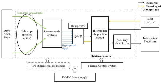
Figure 3.
Schematic diagram of the structure of the satellite-borne LWIR QWIP detection system.
3.1.1. Structure and Parameters of QWIP
The QWIP fabrication process used in the study is described below. In this study, a 30-cycle quantum well infrared detector structure was grown on a GaAs substrate using a molecular beam epitaxy (MBE) method for the face-front type LWIR QWIP using the GaAs/AlGaAs material system [25]. The grown material was tested in advance with optical parameters and single-component flow tests to confirm that the peak response was basically around 9.7 μm. Then, the material was put into the focal-plane chip process flow. The grating was plasma-etched; then, the reflective layer was prepared with the ion beam sputtering method. Finally, the etching of interpixel isolation was performed using the inductively coupled plasma (ICP) etching method [26]. After growing an under-bump metallization (UBM) layer [27], the chip cell was prepared as an In column using thermal evaporation. Then, after scribing, the individual chips were interconnected with the readout circuit using mixed inverted soldering; after interconnection, the indium pillar was reinforced with glue; then, the GaAs substrate was thinned. The finished QWIP focal-plane is shown in Figure 4. The QWIP uses a DI-type readout circuit with a response spectral band of 9.01~10.45 μm [28], encapsulated inside a metal dewar with an integrated pulsed-tube cooler and a target cooling temperature of 41 K. Its main performance indicators are shown in Table 1.
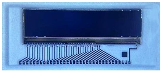
Figure 4.
Physical view of QWIP focal-plane device.

Table 1.
The QWIP’s primary parameters.
3.1.2. Other Subsystem Components
The following describes the subsystem components in the order of target infrared signal transmission. First, the LWIR light emitted from the black body passes through the telescope and is divided by the plane grating. The infrared light, divided into 36 spectral bands, enters the detector window and arrives at the pixels, where photons interact with electrons to produce a current signal, which is collected and processed by a DI-type readout circuit to output an analog signal. Then, the information acquisition circuit follows, amplifies, and low-pass filters the analog signal from the detector, and then enters the ADC with 12 quantization bits to generate the infrared digital signal and transmits this to the FPGA; finally, the FPGA transfers the processed digital signal to the information processor through TLK2711 to store it as image data.
The information acquisition circuit has a temperature measurement module, which is an important design to achieve the objectives of this study. The QWIP has a built-in temperature measurement diode in series with a constant-current source, which allows the real-time temperature of the focal-plane to be measured by the voltage value output from the temperature pin. The selected ADC AD976 has a high accuracy with 16-bit quantization and a quantization accuracy of up to 3 mV. The optics, circuitry, and QWIP components are all within the cooling area affected by the thermal control system, and the cooling temperature of the thermal control is below 200 K, which greatly reduces the effect of the system’s own background radiation [29]. The two-dimensional mechanism is used to adjust the angle between the imaging system and the target and was not in working condition in this study.
3.2. Dark Current Measurement Experiment
As already described in Section 2.3, it was first necessary to carry out calibration experiments on the temperature of the chiller with the temperature measurement pin voltage to calculate the parameters in Equation (9). The refrigeration equipment is shown in Figure 5a using the equipment to adjust multiple chiller temperatures and measure the corresponding temperature measurement pin voltage . The experimental results are shown in Figure 5b, and and have good linearity. The linear fit yields an of and of 1.44 for this chiller. Most of the target cooling temperatures for QWIP in engineering applications are in the range of 40 to 50 K. Therefore, this temperature interval was chosen for the experiments.
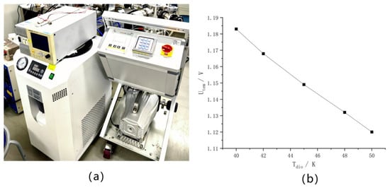
Figure 5.
(a) Calibration equipment for temperature measurement pins of refrigeration machines; (b) Calibration data for temperature measurement pins of refrigeration machines.
With reference to the design of the information acquisition circuit, its specific parameters in Equations (10) and (11) were obtained as shown in Table 2.
Table 2.
Parameters of the temperature measurement module.
The dark current values of the device at 40 K and 50 K were measured at the device preparation stage as and , respectively. By solving Equation (12), it was found that was −0.24 and was −7.02 for this device. The dark current value between 40 and 50 K could be accurately measured. Table 3 shows the dark current values at some temperatures in the range of 40 to 50 K. Figure 6 shows the dark current versus temperature curve, with the horizontal axis being the temperature and the vertical axis being the dark current value .
Table 3.
Dark current values at some temperatures.
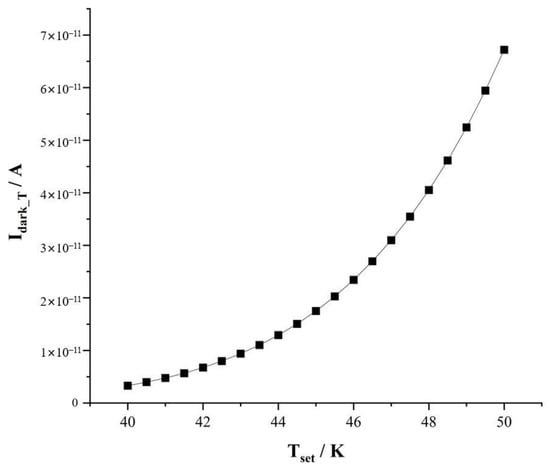
Figure 6.
Dark current values in the range of 40~50 K.
With this method, the focal-plane temperature data can be obtained to monitor the dark current value of a QWIP in satellites in space in real-time, providing more references for the research and development of LWIR QWIP detection systems.
3.3. Long-Wave QWIP Dark Current Noise Correction Experiment
First, the detection system was turned on, and after the chiller stabilized the focal-plane device at the target cooling temperature of 41 K, 1000 frames of image data were acquired continuously facing the 300 K surface-source blackbody. As shown in Figure 7, the image data were processed, and the right side of the vertical axis is the mean response of the detector surface array pixels , the left side of the vertical axis is the acquired temperature response , and the horizontal axis is the sequence number of the frames. It can be clearly seen that the values of and are strongly correlated in the order of frame F. This also confirms that very small temperature fluctuations can cause changes in the dark current in the focal-plane.
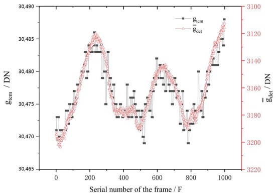
Figure 7.
The relationship between and regarding the serial number of the frames (time order).
Next, the calibration process is described. In the paper, the pixels coordinates were defined using the format (CH, i), where CH is the spectral channel and i is the spatial dimensional coordinate. The data of four pixels from different spectral channels were extracted and used as the target data for calibration. The of this system at a of 41 K is 0.2 K. The in this temperature interval (40.9~41.1 K) was found to be according to Equation (12). The parameters of the target signal preprocessing module in the information acquisition circuit are shown in Table 4. According to the system operation mode, the of Equation (2) was obtained as and is . According to Equations (2), (13) and (14), the response voltage variation value corresponding to this temperature interval can be obtained, the response voltage variation value after preprocessing is , and the quantized value of response voltage after preprocessing is 56.79.
Table 4.
The Information Acquisition Circuit’s parameters.
According to Equation (15), is 4.96. The target data were corrected according to Equation (16), and the corrected data were obtained. As shown in Figure 8, the response values and before and after correction using this method are compared; the horizontal axis is the serial number of the frame, the red curve is the response value after correction, and the black curve is the response value before correction.
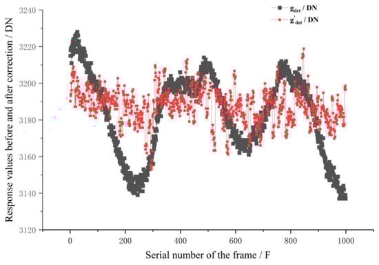
Figure 8.
Response values before and after dark current correction.
By comparison, the fluctuation in the pixel response was significantly reduced after correction using this method, and the temporal noise was reduced. The following is a quantitative analysis of the temporal noise reduction value and its proportion by examining the noise value of the pixel response. The noise reduction effect of this method was examined by comparing the temporal noise before and after the correction of imaging pixels [30]. The noise values before and after correction are calculated as:
where is the noise of a pixel, is the mean response of pixels in f frames, f is the total number of frames (f in this study is 1000), F is the frame serial number, and is the response value of the pixels.
The correction effect is shown in Table 5, and the noise values of the target pixels before and after correction using this method are calculated with Equations (17) and (18). The average reduction in temporal noise after correction was calculated to be 57.69%.
Table 5.
Dark current correction effect.
The remaining noise that was not reduced consists of photonic noise of the background, several types of inherent noise in detectors (including Johnson noise, the generation of composite noise, 1/f noise, and scattered particle noise), the noise of the signal sampling carried out by the information acquisition circuit, and the temporal noise caused by the spectrometer’s temperature change [31].
This method links the two ends of the response model. It is innovative to take a single datum and correct another mixed datum consisting of multiple components. Finally, the prospect of reducing the QWIP dark current noise research is described: (1) the variation in the temperature measurement pin voltage is very small, so a better-performing ADC can be used to sample. (2) The focal-plane temperature data combined with the response of dark pixels for correction may be more suitable.
4. Conclusions
We studied a method for measuring the dark current value of the LWIR QWIP by measuring the focal-plane device temperature, and a dark current noise correction method was also introduced. First, the response model of the LWIR QWIP detection system was introduced, and the dark current model was analyzed in conjunction with the theory. Then, the composition of this detection system was introduced, including the design details of the method closely integrated in the paper. Then, dark current measurement experiments and dark current noise correction experiments were described. Finally, the effect of dark current noise correction was examined, and the total time noise was reduced by 57.69% after correction with this method, which is significant. This method is only applicable to LWIR QWIP detection systems. Because the dark currents of various types of detectors are generated by different mechanisms and depend on different degrees of cooling. The extension of this method to other bands and types of detectors is subject to further validation and improvement. This study included a rigorous theoretical analysis, closely integrated with engineering applications, which will be beneficial to the development of LWIR QWIP remote sensing detection technology.
Author Contributions
Conceptualization, H.D. and Z.G.; methodology, H.D.; software, D.L. and Y.Z.; validation, H.D., Y.W. and Z.G.; formal analysis, H.D.; investigation, H.D.; resources, Y.Z. and J.X.; data curation, Z.G. and H.D.; writing—original draft preparation, H.D.; writing—review and editing, D.S. and J.X.; visualization, D.L.; funding acquisition, D.S. All authors have read and agreed to the published version of the manuscript.
Funding
This research was funded by the Major Program of National Natural Science Foundation of China, grant number 42192582, and the National Key Research and Development Program of China, grant number 2016YFB0500400.
Institutional Review Board Statement
Not applicable.
Informed Consent Statement
Not applicable.
Data Availability Statement
Not applicable.
Conflicts of Interest
The authors declare no conflict of interest.
References
- Shi, Y.L. Choice and development of the third-generation infrared detectors. Infrared Technol. 2013, 35, 1–8. [Google Scholar]
- Ye, Z.H.; Li, F.H.; Wang, J.D.; Chen, X.; Sun, S.H.; Liao, Q.J.; Huang, A.B.; Li, F.; Zhou, S.M.; Lin, J.M.; et al. Recent hotspots and innovative trends of infrared photon detectors. J. Infrared Millim. Waves 2022, 41, 15–39. [Google Scholar]
- Bhan, R.K.; Dhar, V. Recent infrared detector technologies, applications, trends and development of HgCdTe based cooled infrared focal plane arrays and their characterization. Opto-Electron. Rev. 2019, 27, 174–193. [Google Scholar] [CrossRef]
- Plis, E.A. InAs/GaSb type-II superlattice detectors. Adv. Electron. 2014, 2014, 246769. [Google Scholar] [CrossRef]
- Huang, W.; Ji, H. Effect of environmental radiation on the long-wave infrared signature of cruise aircraft. Aerosp. Sci. Technol. 2016, 56, 125–134. [Google Scholar] [CrossRef]
- Hołyńska, M.; Tighe, A.; Semprimoschnig, C. Coatings and thin films for spacecraft thermo-optical and related functional applications. Adv. Mater. Interfaces 2018, 5, 1701644. [Google Scholar] [CrossRef]
- Sharma, A.; Sridhara, N. Degradation of thermal control materials under a simulated radiative space environment. Adv. Space Res. 2012, 50, 1411–1424. [Google Scholar] [CrossRef]
- Nana, X.; Feng, Y.; Zhenhua, Z. Thermal design and validation of a geosynchronous orbit infrared camera. Infrared Laser Eng. 2021, 50, 170–177. [Google Scholar]
- Lu, Y.; Shao, Q.; Yue, H.; Yang, F. A review of the space environment effects on spacecraft in different orbits. IEEE Access 2019, 7, 93473–93488. [Google Scholar] [CrossRef]
- Feng, Y.; Nana, X.; Zhenming, Z. On-orbit temperature analysis and thermal design optimization for camera on GF-4 satellite. J. Beijing Univ. Aeronaut. Astronaut. 2021, 47, 177–186. [Google Scholar]
- Wang, G.Q.; Shen, X.; Wang, W.C.; Wang, B.Y.; Hu, B.T. On board adaptation of temperature of the FY-4 meteorological satellite radiation imager. J. Infrared Millim. Waves 2018, 37, 540–544. [Google Scholar]
- Johnson, W.R.; Hook, S.J.; Mouroulis, P.Z.; Wilson, D.W.; Gunapala, S.D.; Hill, C.J.; Mumolo, J.M.; Eng, B.T. QWEST: Quantum Well Infrared Earth Science Testbed. In Proceedings of the Imaging Spectrometry XIII, San Diego, CA, USA, 12–13 August 2008; pp. 65–74. [Google Scholar]
- McCorkel, J.; Montanaro, M.; Efremova, B.; Pearlman, A.; Wenny, B.; Lunsford, A.; Simon, A.; Hair, J.; Reuter, D. Landsat 9 Thermal Infrared Sensor 2 Characterization Plan Overview. In Proceedings of the IGARSS 2018-2018 IEEE International Geoscience and Remote Sensing Symposium, Valencia, Spain, 22–27 July 2018; pp. 8845–8848. [Google Scholar]
- Reuter, D.C.; Richardson, C.M.; Pellerano, F.A.; Irons, J.R.; Allen, R.G.; Anderson, M.; Jhabvala, M.D.; Lunsford, A.W.; Montanaro, M.; Smith, R.L. The Thermal Infrared Sensor (TIRS) on Landsat 8: Design overview and pre-launch characterization. Remote Sens. 2015, 7, 1135–1153. [Google Scholar] [CrossRef]
- Liu, H.; Steele, A.; Buchanan, M.; Wasilewski, Z. Dark current in quantum well infrared photodetectors. J. Appl. Phys. 1993, 73, 2029–2031. [Google Scholar] [CrossRef]
- Rogalski, A. Quantum well photoconductors in infrared detector technology. J. Appl. Phys. 2003, 93, 4355–4391. [Google Scholar] [CrossRef]
- Levine, B.F. Quantum-well infrared photodetectors. J. Appl. Phys. 1993, 74, R1–R81. [Google Scholar] [CrossRef]
- Andresen, B.F.; Jhabvala, M.; Fulop, G.F.; Reuter, D.; Choi, K.; Norton, P.R.; Sundaram, M.; Jhabvala, C.; La, A.; Waczynski, A.; et al. The QWIP focal plane assembly for NASA’s Landsat Data Continuity Mission. In Proceedings of the Infrared Technology and Applications XXXVI, Orlando, FL, USA, 5–9 April 2010. [Google Scholar]
- Du, H.; Xu, J.; Yin, Z.; Chai, M.; Sun, D. Dark Current Noise Correction Method Based on Dark Pixels for LWIR QWIP Detection Systems. Appl. Sci. 2022, 12, 12967. [Google Scholar] [CrossRef]
- Zhang, W.K.; Chen, H.L.; Ding, R.J. Long wavelength infrared readout circuit with background suppression function. Infrared Laser Eng. 2021, 50, 20200266. [Google Scholar] [CrossRef]
- Zhang, C.J.; Zhang, H.; Chang, Y.G.; Chen, C.C. A review of radiometric calibration methods for optical remote sensors of Landsat series satellites. J. Remote Sens. 2015, 19, 719–732. [Google Scholar]
- Li, C.L.; Lin, C.; Chen, X.W.; Ding, X.Z.; Wang, J.Y. A satellite-borne long-wave infrared focal plane imaging system. Infrared Laser Eng. 2012, 41, 2253–2260. [Google Scholar]
- Wang, J.Y.; Xu, W.M.; Yuan, L.Y.; Lin, Y.; He, Z.P.; Liu, J. Background radiation suppression of a thermal infrared hyperspectral imaging system. J. Infrared Millim. Waves 2010, 29, 419–423. [Google Scholar]
- Pan, J.L.; Fonstad, C.G., Jr. Theory, fabrication and characterization of quantum well infrared photodetectors. Mater. Sci. Eng. R Rep. 2000, 28, 65–147. [Google Scholar] [CrossRef]
- Arthur, J.R. Molecular beam epitaxy. Surf. Sci. 2002, 500, 189–217. [Google Scholar] [CrossRef]
- Lee, J.; Devre, M.; Reelfs, B.; Johnson, D.; Sasserath, J.; Clayton, F.; Hays, D.; Pearton, S. Advanced selective dry etching of GaAs/AlGaAs in high density inductively coupled plasmas. J. Vac. Sci. Technol. A Vac. Surf. Film. 2000, 18, 1220–1224. [Google Scholar] [CrossRef]
- He, M.; Chen, Z.; Qi, G. Solid state interfacial reaction of Sn–37Pb and Sn–3.5 Ag solders with Ni–P under bump metallization. Acta Mater. 2004, 52, 2047–2056. [Google Scholar] [CrossRef]
- Johnson, J.F. Direct injection readout circuit model. In Infrared Readout Electronics II; Fossum, E.R., Ed.; SPIE: Bellingham, WA, USA, 1994; pp. 120–129. [Google Scholar]
- Huang, F.; Shen, X.; Li, G.; Wang, G.; Zhao, Z. Influence of background radiation on space target detection in the long wave infrared range. Opt. Eng. 2012, 51, 086402. [Google Scholar] [CrossRef]
- Wolfe, W.L. Introduction to Infrared System Design; SPIE Press: Tucson, AR, USA, 1996; Volume 24. [Google Scholar]
- Kolev, P.; Deen, M.; Liu, H.; Li, J.; Buchanan, M.; Wasilewski, Z. Asymmetry in the dark current low frequency noise characteristics of B–B and B–C quantum well infrared photodetectors from 10 to 80 K. J. Appl. Phys. 2000, 87, 2400–2407. [Google Scholar] [CrossRef]
Disclaimer/Publisher’s Note: The statements, opinions and data contained in all publications are solely those of the individual author(s) and contributor(s) and not of MDPI and/or the editor(s). MDPI and/or the editor(s) disclaim responsibility for any injury to people or property resulting from any ideas, methods, instructions or products referred to in the content. |
© 2023 by the authors. Licensee MDPI, Basel, Switzerland. This article is an open access article distributed under the terms and conditions of the Creative Commons Attribution (CC BY) license (https://creativecommons.org/licenses/by/4.0/).