Abstract
In this paper, a solution is proposed to the problem of the unequal phase imbalance of output voltage caused by a three-phase, four-wire, split capacitor inverter when the load is unbalanced. First, the triple-loop control strategy was used to solve the unequal amplitude problem. This method used the feedforward + feedback composite control strategy on the inductor current inner-loop and voltage mid-loop to decrease the disturbance of the power and load. And the Root Mean Square (RMS) of voltage on the outer-loop completed the control of amplitude for the three-phase voltage. Second, to solve the imbalanced phase problem, the imbalance operation mechanism of the three-phase four-wire inverter was analyzed. It is known from the analysis that the phase imbalance is related to the DC-side splitting capacitance. The function relations between the DC-side capacitance and phase angle between each phase was simulated by MATLAB. But, it was too complicated to calculate the magnitude of the capacitance value through the functional relationship. In order to simplify the design of the DC-side splitting capacitor, the relations among the imbalanced current, the voltage fluctuations of the DC-side capacitor and the harmonics of load voltage were analyzed. In addition, by following the requirement of the national standard about the harmonics of load voltage, a DC-side capacitor design was mentioned to decrease the influence of imbalanced phase. Finally, simulation and experimental results show that the three-phase load voltage is stable, the THD value is less than 3%, and three-phase voltage unbalance is less than 2%, thus verifying the effectiveness of the proposed DC-side split capacitor design and control strategy.
1. Introduction
Traditional three-phase, three-wire inverters can cause undervoltage or overvoltage in one phase when carrying unbalanced loads [1,2,3]. To improve the output voltage balance of three-phase inverters with unbalanced loads, the main methods used in the literature can be divided into the following four categories: combined three-phase inverters, three-phase four-bridge arm inverters, D/Y transformers on the inverter and load side and split-capacitor, three-phase, four-wire inverters. Three-phase, four-wire split-capacitor inverters can also be widely used in grid-connected systems for power quality improvement [4,5,6]. Literature [4] proposes a current–feedback-based impedance shaping strategy to suppress the high-frequency resonance caused by the split-sequence control. Literature [5] analyses the three-phase four-wire split-capacitor inverter and three-phase four-bridge-arm inverter and also presents several cases of small-signal instability caused by the positive sequence, negative sequence or zero sequence. Literature [6] proposes an impedance shaping method based on complex filters and combined differential elements to improve the stability of grid-connected systems. But the above-mentioned literature does not give a method of selecting the splitting capacitor on the DC-side. Literature [7,8] proposes a combined three-phase inverter with a circuit using three independent H-bridges so that the inter-phase circuits are independent of each other, with sigmoid P-f sag control in literature [7] and split-sequence and repetitive control in literature [8]. Literature [9,10] proposes a three-phase four-bridge arm inverter with the neutral point of the three-phase load connected to the mid-point of the fourth bridge arm as a means of controlling unbalanced currents; literature [9] uses an improved positive-sequence, negative-sequence and zero-sequence independent control strategy that is applicable to the three-phase four-bridge arm, and literature [10] proposes a control specific to the three-phase four-bridge arm. Literature [11,12] proposes the insertion of a D/Y transformer between the conventional three-phase, three-wire inverter and the load to achieve electrical isolation between the input and output. Literature [11] controls the positive and negative sequence components of the voltage, while literature [12] uses split-phase control. All of the above-mentioned control methods achieved good control results, but their circuit structures are relatively complex. Literature [13,14,15] proposes split-capacitor three-phase four-wire inverters, where the neutral point of the three-phase load is connected to the mid-point of the DC-side capacitor to provide a path for the unbalanced current. Literature [13] uses a DSTATCOM control method based on a dual-loop controller. Literature [14] compensates for negative and zero sequence currents, and literature [15] uses split-sequence sag control. The above control enables the inverter to output a three-phase-balanced voltage. In the above references, the circuit structure used is simple, but the modelling and analysis of the control method is relatively cumbersome, and none of them analyses the value of the capacitance of the DC-side division.
In this paper, a split capacitor three-phase four-wire inverter is used. The appropriate DC-side capacitance is selected by means of calculation and analysis. And the use of a feedforward + feedback + RMS three-closed-loop composite control strategy means that the output voltage meets national standards. The effectiveness of this method has been verified through simulation and experimentation. The circuit structure is simple, the cost is low, the control method is simple, and the system requirements can be met at the same time.
2. Three-Closed-Loop Control of an Unbalanced Three-Phase Four-Wire Inverter
2.1. Control Principle of a Three-Phase Four-Wire Inverter
The split-capacitor three-phase, four-wire inverter circuit is shown in Figure 1, and the control principle is shown in Figure 2. The voltage outer loop is operated by collecting the three-phase voltages for RMS values and then making a difference with the target value for PI regulation and multiplying the regulated output with the unit sine wave sin ωt to obtain the instantaneous command voltages ua, ub and uc, which are transformed by abc–dq coordinates to generate and . Then, voltage loop PI regulation and feedforward decoupling generate the command currents and for the current’s inner loop. The difference between the commanded current and the coordinate transformed actual currents idL and iqL for the PI regulation of the current inner loop and feedforward decoupling generates urd and urq. Finally, the SPWM technique is used to generate PWM waves to complete the control of the three-phase, four-wire inverter, three-closed-loop system [16].
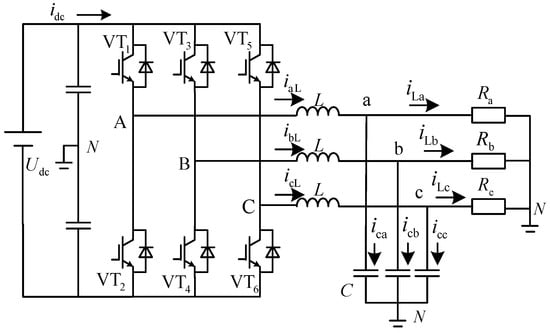
Figure 1.
Split-capacitor three-phase four-wire inverter circuit.
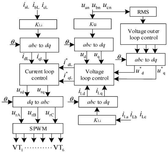
Figure 2.
Three-closed-loop control block diagram.
2.2. Modelling of Three-Phase Four-Wire Inverter
The main circuit of a three-phase, four-wire inverter using an LC filter circuit is shown in Figure 1. IaL, ibL and icL are the currents flowing through the filter inductor; iLa, iLb and iLc are the currents flowing through the load; ica, icb and icc are the currents flowing through the filter capacitor, and idc is the DC-side current.
The voltage of the filter inductor is transformed by the abc–dq coordinates as follows:
In Equation (1), is the gain of the SPWM modulation in the frequency domain, and urd and urq are the modulating wave voltages converted to the dq coordinate system.
Similarly, the current in the filter capacitor is transformed by the abc–dq coordinates as follows:
2.3. Control Analysis of Three-Phase Four-Wire Inverters
2.3.1. Current Loop Control
It is assumed that the system’s voltage gain (the ratio of the voltage Hall) is Ku and the current gain (the ratio of the current Hall) is KLi. According to Equation (1), the d-axis current control block diagram is shown in Figure 3. A feedforward signal is added to eliminate the current coupling between the d and q axes. The addition of another feedforward control signal is used to eliminate voltage disturbances to the current circuit. The current’s compensation link can be designed using the P, PI or PI + LPF (low-pass filter) design; this study used the design PI + LPF (low-pass filter) method for analysis.
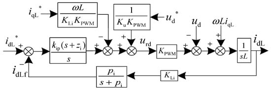
Figure 3.
The current loop d-axis control block diagram.
Similarly, according to Equation (1), the q-axis current control block diagram is shown in Figure 4.
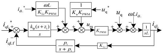
Figure 4.
Current loop q-axis control block diagram.
Open Loop Transfer Function of the Current Loop
The open loop transfer function of the current loop system as follows:
In Equation (3), is the pole value of the low-pass filter, zi is the zero value of the PI controller, and kip is the scaling factor of the current inner loop.
is the transfer function of the low-pass filter, where . The main reason for adding a low-pass filter to the current output’s feedback is to suppress the interference of the switching signals.
Selection of the Zero Pole of the Compensation Link in the Current Link
It is known from the principle of automatic control that, in order to meet the steady-state requirements of the system, the gain in the low frequency band of the Porter diagram should be sufficiently large after compensation. To ensure a suitable phase angle margin, the slope of the mid-band gain is usually taken to be −20 dB/dec. To suppress high-frequency interference signals, the slope of the high-band gain is −20dB/dec. Therefore, the selection of the zero pole of the transfer function of the compensation link is crucial.
The compensated crossing frequency value is set as fic = (1/8~1/10) fs, based on experience. Zero frequency is fiz = fic/3. The pole frequency of the filter link is fip = fs/2, where fs is the switching frequency.
Calculation of Current Loop Compensation Link Parameters
The scale factor kip of the current loop can be derived from the amplitude of the compensated transfer function at the crossing frequency fic as one. The integration factor kii is derived from .
2.3.2. Voltage Loop Control
According to Equation (2), the voltage loop control block diagram is shown in Figure 5 and Figure 6. Assuming that the response bandwidth of the current loop is greater than or equal to four times the response bandwidth of the voltage loop, the current loop can be considered a proportional link with a gain of one when analyzing the voltage loop [17]. The voltage loop control, like the current loop control, is in the form of feedforward + feedback. The collected load current is added to the command current as a way of eliminating the interference of the load current to the voltage loop. and are added to eliminate the current ( and ) interference of the filter capacitor.
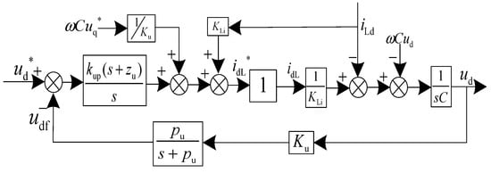
Figure 5.
Voltage loop d-axis control block diagram.
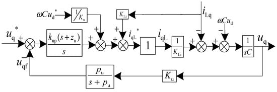
Figure 6.
Voltage loop q-axis control block diagram.
Open Loop Transfer Function of the Voltage Loop
According to Figure 5 and Figure 6, the open-loop transfer function of the voltage loop designed with PI + LPF is as follows:
In Equation (4), pu is the pole value of the filter link, zu is the zero value of the PI regulation, and kup is the scale factor of the current loop.
As with the current inner loop, is the transfer function of the low-pass filter, where . This has the same main function as the low-pass filter in the current loop, both of which are designed to eliminate interference from switching signals.
Selection of the Zero Pole of the Compensation Link in the Voltage Link
The selection of the zero pole of the voltage outer loop compensation link is similar to the selection of the zero pole of the current inner loop compensation link. When selecting the value of the zero pole of the outer voltage loop compensation link, the value of the zero pole of the inner current loop is used as a reference.
To meet the requirements for the amplitude and phase margin, the compensated crossing frequency fuc = fic/4, the zero frequency fuz = fuc/3, and the filter link pole frequency fup = 2fuc can be set.
Calculation of Voltage Loop Compensation Link Parameters
The scale factor kup of the voltage loop can be derived from the amplitude of the compensated transfer function at the crossing frequency fuc as one. The integration factor kui is derived from .
2.3.3. Voltage RMS Outer Loop Control
To ensure that the output of the inverter has good voltage regulation and that the load voltage amplitude remains in balance when the three-phase load is unbalanced, the RMS control loop can be added to the voltage loop, as shown in Figure 7. The collected three-phase voltages are subjected to an RMS calculation to obtain urms and then compared with the reference value of the RMS value . After PI adjustment, the amplitude correction signal um is generated. um is then multiplied by the unit sine wave sin ωt to obtain the three-phase instantaneous command voltages, which are transformed by coordinates to obtain the command voltages and .
Figure 7.
Voltage RMS outer loop control block diagram.
3. DC-Side Capacitance Analysis
3.1. Effect of DC-Side Capacitance on Phase between Phases
Simulation software was used to simulate the split-capacitor three-phase four-wire inverter. An analysis of the experimental results shows that the three-closed-loop control keeps the amplitude of the three-phase output voltage stable, and the variation in the capacitance on the DC-side causes deviations between phases. Through the Cftool toolbox in MATLAB 2019B, the capacitance of the DC-side capacitor and the phase of the output voltage are fitted as a function, and thus, the DC-side capacitance is obtained as a function of the phase between each phase, using the parameters in Table 1 for simulation.

Table 1.
Simulation model parameters.
After fitting, it can be obtained that the DC-side capacitance is related to the phase of phase AB, as shown in Equation (5), and its function curve is shown in Figure 8.
Figure 8.
Phase function curve between the DC-side capacitance and AB phase.
The DC-side capacitance is related to the phase between the BC phases as a function of Equation (6), and its function curve is shown in Figure 9.
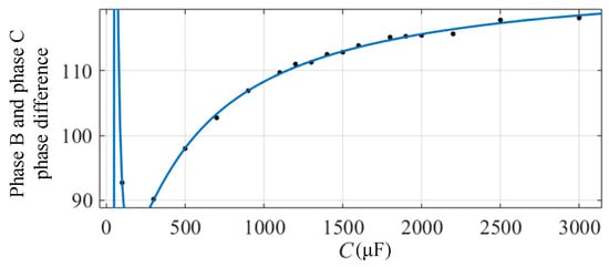
Figure 9.
Phase function curve between the DC-side capacitance and BC phase.
The DC-side capacitance is related to the phase between the CA phases as a function of Equation (7), and its function curve is shown in Figure 10.
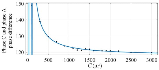
Figure 10.
Phase function curve between the DC-side capacitance and CA phase.
The DC-side capacitance can be designed according to the fitted function curve, and the DC-side capacitance can be selected to meet the system requirements. The calculated capacitance values on the DC-side obtained by this method do not differ significantly from those obtained using the method mentioned below. However, this design method is tedious, computationally intensive and has limitations. In order to obtain the size of the DC-side capacitance more easily, the following DC-side capacitance design method is proposed.
3.2. Effect of DC Voltage Fluctuations on Load Voltage
Due to the presence of the midline, when the three-phase load is unbalanced, the unbalanced current charges and discharges the DC-side capacitor, which, in turn, causes fluctuations in the DC-side capacitance voltage [18,19], which can be expressed as follows:
In Equation (8), uc is the AC component of the capacitive voltage on the DC-side caused by the midline current, which lags the midline current by 90° in the phase, and in order not to lose generality the following is set:
Ucm is the amplitude of the capacitive voltage fluctuation on the DC-side, using SPWM control and assuming a modulation system of m. The duty cycle can be expressed as follows:
Due to the fluctuation in the capacitor voltage on the DC-side, combined with Equation (8), the output load phase voltage can be expressed as follows:
The three-phase load phase voltage can be expressed as follows:
Transforming the above equation further provides the following:
In Equation (13), the first term is the positive sequence’s fundamental component, the second term is the second harmonic, and the third term is the DC component. In a three-phase, four-wire inverter, unbalanced currents caused by unbalanced loads flow through the center line, resulting in fluctuations in the capacitance voltage on the DC-side. The DC-side capacitor experiences voltage fluctuations, which, in turn, cause second harmonics and DC components in the load voltage, so the DC-side capacitor design directly affects the system’s performance and phase imbalance. Usually, the larger the capacitance, the smaller the voltage fluctuation. In order to effectively suppress voltage fluctuations, the capacitance value can be sized according to the requirements of the voltage fluctuations of the capacitor on the DC-side. And the magnitude of the DC-side’s capacitance voltage fluctuation is related to the unbalanced current.
3.3. Effect of Unbalanced Current on Voltage Fluctuations in the DC-Side Capacitor
For the three-phase, four-wire inverter, when considering the effect of the unbalanced current on the DC-side capacitor voltage, the DC-side voltage Udc can be considered to be inactive, and the equivalent circuit of the system is shown in Figure 11.
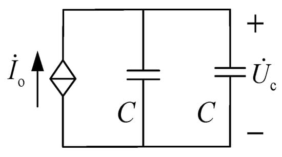
Figure 11.
Equivalent circuit diagram when charging and discharging a capacitor with an unbalanced current.
Let the three-phase unbalanced currents be represented by , and , then the midline currents as follows:
Neglecting the higher harmonics and DC components of the system and considering only the fundamental components, the capacitor voltage amplitude is as follows:
In Equation (15), Io is the amplitude of the unbalanced current.
3.4. Determination of DC-Side Capacitance
According to the requirements of the national standard GB/T14549-1993 for harmonics in the load voltage (even harmonic content rate of 2%) and Formula (13), we can obtain the following:
According to the maximum unbalance of the system, the current Io in the center line can be obtained according to Equation (14). Combining Equations (15) and (17), the value of the capacitance on the DC-side is as follows:
4. Simulation and Experimental Validation
To verify the correctness of the design of the DC-side capacitance and the effectiveness of the three-closed-loop control when the load of a three-phase four-wire inverter is unbalanced, a MATLAB/Simulink model was built for simulation and analysis. The model was built according to the parameters in Table 1, and the loads were adjusted to Ra = 30 Ω, Rb = 20 Ω and Rc = 15 Ω for verification. The higher harmonics and DC components of the voltage content were ignored in the calculation of the unbalanced current, and only the fundamental component was considered. Also, according to Equation (16), the amplitude of the DC-side capacitance voltage fluctuation was selected in accordance with the critical value of the national standard. In order to be better than the critical values specified in the national standard, the actual values were, therefore, taken to be approximately 1 to 1.2 times the theoretical calculated values.
The unbalanced current was calculated to be Io = 2.5 A. According to the splitting capacitance selection method proposed in this paper, after calculation, it is known that the splitting capacitance on the DC-side was C = 919 μF. When the DC-side capacitance was taken to be 500 μF (less than 919 μF), the load voltage waveforms of the system from startup to stabilization and from load fluctuation to stabilization are shown in Figure 12. From the graph it can be seen that the phase deviation was large.
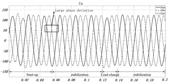
Figure 12.
Simulated waveform with a capacitance value of 500 μF.
When the DC-side capacitance was taken to be 919 μF, the load voltage waveforms of the system from startup to stabilization and from load fluctuation to stabilization are shown in Figure 13. From the graph it can be seen that the phase deviation was small.
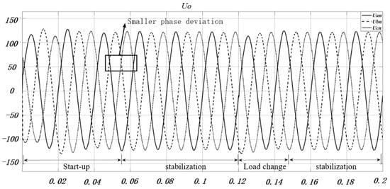
Figure 13.
Simulated waveform with a capacitance value of 919 μF.
Through the above simulation experiments, it can be shown that the three closed-loop control strategy effectively ensures the stability of the load voltage, and the DC-side capacitance selection method proposed in this paper can effectively suppress the phase error.
Within 0–0.04, the time from system start-up to stabilization, and at 0.12 s, the load voltage changed and Rb changed. from 20 Ω to 40 Ω, and, in one cycle, the system stabilized.
According to the parameters in Table 1, the experimental prototype was built, the size of the load was changed, and the load voltage waveform, THD value and voltage unbalance (%) were observed.
When the three-phase load was balanced (Ra = Rb = Rc = 20 Ω) and the system was stabilized, the load power was 1084 W; at this time, the load voltage waveform and THD value are shown in Figure 14, and the voltage unbalance is shown in Figure 15.
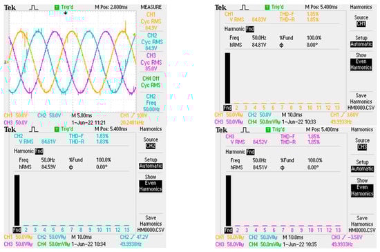
Figure 14.
Voltage waveform and THD value when the load is balanced.
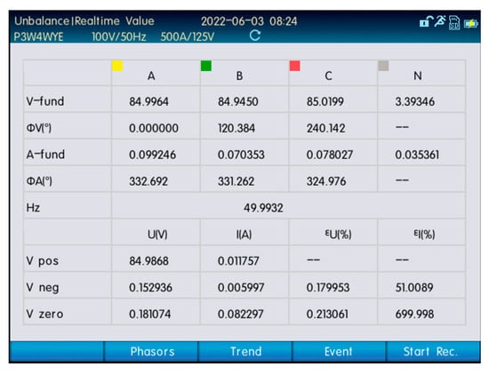
Figure 15.
Voltage unbalance when the load is balanced.
Case 1: The three-phase load was adjusted to Ra = 30 Ω, Rb = 20 Ω, Rc = 15 Ω; at this time, the load power was 1082 W, the unbalanced current was calculated to be Io = 2.5 A, the DC-side capacitance was C = 919 μF and the nominal value was taken as 1100 μF capacitance. The difference between nominal and actual values should be noted in the experiment. The load voltage waveform and THD values after system stabilization are shown in Figure 16, and the voltage unbalance is shown in Figure 17.
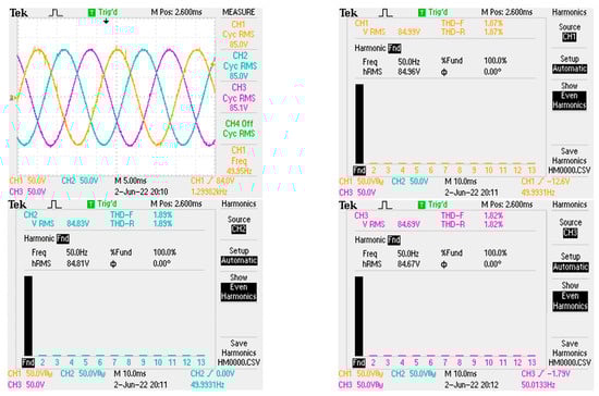
Figure 16.
Case 1: load voltage waveform and THD value.
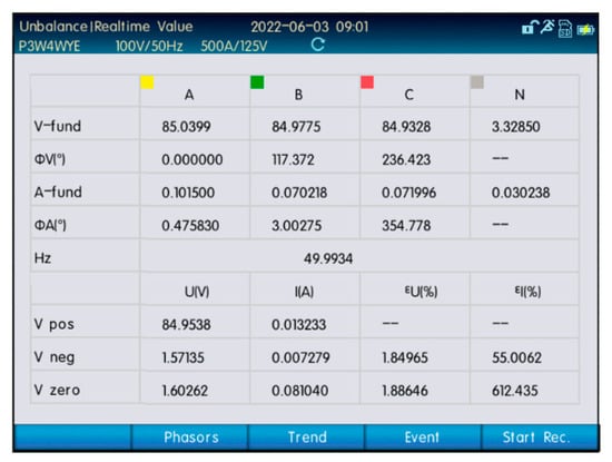
Figure 17.
Case 1: voltage unbalanced.
Case 2: The three-phase load was adjusted to Ra = 10 Ω, Rb = 20 Ω, Rc = 10 Ω; at this time, the load power was 1806 W, the unbalanced current was calculated to be Io = 4.2 A, the DC-side capacitance was C = 1592 μF, and the nominal value was taken as 1100 μF capacitance (connected to 1000 μF with two 450 μF in parallel). The load voltage waveform and THD values after system stabilization are shown in Figure 18, and the voltage unbalance is shown in Figure 19.
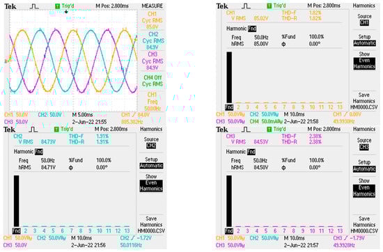
Figure 18.
Case 2: load voltage waveform and THD value.
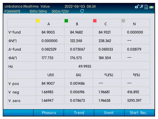
Figure 19.
Case 2: voltage unbalanced.
Case 3: The three-phase load was adjusted to Ra = 30 Ω, Rb = 20 Ω, Rc = 10 Ω; at this time, the load power was 1324 W, the unbalanced current was calculated to be Io = 5.1 A, the DC-side capacitance was C = 1912.5 μF, and the nominal value was taken as 2200 μF capacitance. The load voltage waveform and THD values after system stabilization are shown in Figure 20, and the voltage unbalance is shown in Figure 21.
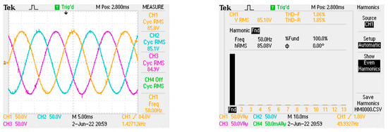
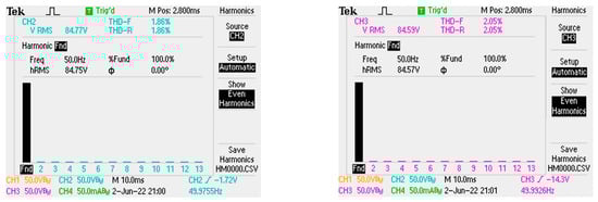
Figure 20.
Case 3: load voltage waveform and THD value.
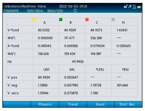
Figure 21.
Case 3: voltage unbalanced.
Through the above four sets of experiments, it can be seen that the three closed-loop control strategy can ensure that the amplitude of the three-phase load voltage is equal; at the same time, according to the Chinese national standard for the second harmonic content of the requirements of the DC-side of the splitting capacitance, it can effectively inhibit the phase imbalance, and ultimately guarantee to ensure that the output of the three-phase load voltage imbalance degree is less than 2%.
Literature [19] suggests that as the current periodically charges and discharges the split capacitor on the DC-side, causing the split capacitor to be unbalanced, this, in turn, affects the output voltage waveform. From the analysis it was obtained that the amount of voltage deviation after stabilization of the system is as follows:
In Equation (19), is the amount of split capacitor voltage deviation and is the magnitude of the charge/discharge current. Since a reasonable range of voltage fluctuations for the DC-side splitting capacitor is not given, the selected capacitor may not satisfy the system’s need for phase rejection.
The simulation and experimental results show that, according to the method proposed in this paper, the voltage unbalance meets the requirements of the national standard GB/T 15543-2008 when the load is unbalanced, and in practical applications, the capacitor selection leaves a certain margin. The above experiments were all conducted on the experimental prototype shown in Figure 22, which included a DC power supply, a three-phase bridge, an LC filter circuit, a voltage–current Hall, a digital signal processor TMS320F28335, a TPS2014B oscilloscope to observe the load voltage waveform, and a UT285A three-phase power quality analyzer to observe the voltage unbalance.
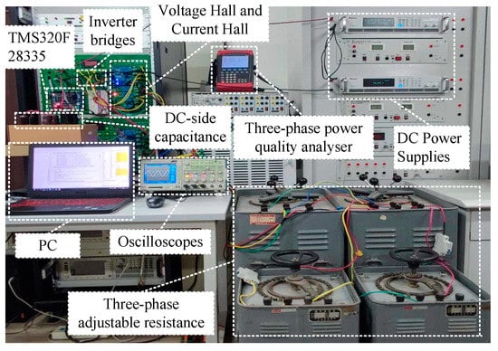
Figure 22.
Experimental prototype.
5. Conclusions
In this paper, a feedforward + feedback + RMS triple-closed-loop composite control strategy and compensation correction network were designed. The influence of the DC voltage fluctuation on the load voltage was studied. Furthermore, the relationship between the load current unbalance and DC-side capacitance voltage fluctuation was analyzed. A design method for DC-side capacitance was proposed. The simulation and experimental results show that the three-phase, four-wire inverter with triple-closed-loop composite control is able to keep the output three-phase voltage balanced and the THD value less than 3% when the load is unbalanced, which meets the national standard. Simulation and experimental results verify the effectiveness of the control method and the correctness of the capacitor design. A reference is provided for the control and DC-side capacitor design of the three-phase four-wire inverter circuit.
Author Contributions
F.W. and S.W. contributed to research idea of the study; methodology, F.W.; simulation, B.M.; validation, B.M., S.P. and M.L.; data curation, S.P. and M.L.; writing the original preparation, B.M.; writing review, F.W. and editing, S.W.; project administration, F.W.; funding acquisition, S.W. All authors have read and agreed to the published version of the manuscript.
Funding
This research was funded by the National Natural Science Foundation (No. 62073297, No. U1813201), Programs for Science and Technology Development of Henan (222102210019, 222102520024, 212102210080), Natural Science Foundation of Henan (222300420595).
Institutional Review Board Statement
Not applicable.
Informed Consent Statement
Not applicable.
Data Availability Statement
Data are contained within the article.
Acknowledgments
The authors would like to thank the Henan Province Science and Technology R&D projects, the Young Backbone Teachers in Henan Province, and the National Natural Science Foundation for their support of this work.
Conflicts of Interest
The authors declare no conflict of interest.
References
- Guo, X.H.; Chang, C.W.; Chang-Chien, L.R. An Automatic Voltage Compensation technique for Three-Phase Stand-Alone Inverter to serve unbalanced or nonlinear load. In Proceedings of the IEEE 2nd International Future Energy Electronics Conference (IFEEC), Taipei, Taiwan, 1–4 November 2015; pp. 1–6. [Google Scholar]
- Fan, M.; Liu, H.K. Research on control method of load under the strong disturbance of wave power inverter. Electr. Meas. Instrum. 2015, 52, 78–81. [Google Scholar]
- Luo, J.; Zhang, H.; Zhang, S.; Wu, W.; Ouyang, H.; Chen, Y. Modeling and characteristic analysis of sequential impedance of three-phase off-grid inverter under unbalanced load. Power Syst. Prot. Control 2020, 48, 30–40. [Google Scholar]
- Feng, G.; Ye, Z.; Xia, Y.; Nian, H.; Huang, L.; Wang, Z. High Frequency Resonance Suppression Strategy of Three-Phase Four-Wire Split Capacitor Inverter Connected to Parallel Compensation Grid. Energies 2022, 15, 1486. [Google Scholar] [CrossRef]
- Feng, G.; Ye, Z.; Xia, Y.; Huang, L.; Wang, Z. Impedance Modeling and Stability Analysis of Three-Phase Four-Wire Inverter with Grid-Connected Operation. Energies 2022, 15, 2754. [Google Scholar] [CrossRef]
- Yang, L.; Cao, T.; Cai, Z.; Xia, X.; Jia, C.; Dong, X.; Zhang, S. Stability Analysis and Robust Control Method for LCL-Type Three-Phase Four-Wire Split Capacitor Inverter Considering Zero-Sequence Loop. Electronics 2022, 11, 3286. [Google Scholar] [CrossRef]
- Ren, B.Y.; Zhao, X.R.; Sun, X.D.; Yang, H. Improved droop control based three-phase combined inverters for unbalanced load. Power Syst. Technol. 2016, 40, 1163–1168. [Google Scholar]
- Yang, K.; Chen, L.; Chen, G.Z. Individual sequence control of DSTATCOM compensation for unbalanced load. Electr. Power Autom. Equip. 2012, 32, 36–41. [Google Scholar]
- Zhou, X.; Jin, X.M.; Tang, F. Improved Sequence Decomposition Control Strategy for Three-phase Four-leg Inverter with Unbalanced Load. High Volt. Eng. 2014, 40, 2504–2512. [Google Scholar]
- Sun, C.; Ma, W.M.; Lu, J.Y. Analysis of the Unsymmetrical Output Voltages Distortion Mechanism of Three-Phase Inverter and Its Corrections. Proc. CSEE 2006, 26, 57–64. [Google Scholar]
- Xu, S.G. Research into Control Method of Three-phase Inverter Power Supply Under Unbalanced Load. J. Chong Qing Norm. Univ. (Nat. Sci.) 2009, 26, 103–107. [Google Scholar]
- Cao, T.Q.; Qi, Q.; Wang, J. Study on unbalanced load of three-phase inverter. Electr. Mach. Control 2012, 16, 50–55. [Google Scholar]
- Zhou, C.; Zheng, Y.H.; Wang, X.; Li, L.X. Control strategy based on dual-loop controller for split-capacitor-type three-phase four-wire DSTATCOM. Electr. Power Autom. Equip. 2014, 34, 114–121. [Google Scholar]
- Shan, T.M.; Yang, R.G. Reactive power compensation for unbalanced current. Electr. Power Autom. Equip. 2004, 24, 26–29. [Google Scholar]
- Cheng, J.; Zhao, B.; Chen, X. Droop Control of Three-Phase Four-Wire Parallel Inverters under Unbalanced Load Condition. Trans. China Electrotech. Soc. 2018, 33, 4790–4801. [Google Scholar]
- Wang, Y.B. Principles, Design and Engineering Practice of Advanced Power Electronics Technology; Shandong University Press: Shandong, China, 2020. [Google Scholar]
- Xu, D.H. Power Electronic System Modeling and Control; China Machine Press: Beijing, China, 2006. [Google Scholar]
- Pei, X.J.; Chen, C.; Kang, Y. Analysis of Voltage Ripple and Design for DC-Link Capacitor in Three-Phase Voltage Source Inverters. Trans. China Electrotech. Soc. 2014, 29, 254–259+269. [Google Scholar]
- Chen, D.H.; Xie, S.J. Research on Current-Mode Control Half-Bridge Inverter(I)—Voltage Un-Balance of Input Capacitors. Trans. China Electrotech. Soc. 2004, 19, 85–88+51. [Google Scholar]
Disclaimer/Publisher’s Note: The statements, opinions and data contained in all publications are solely those of the individual author(s) and contributor(s) and not of MDPI and/or the editor(s). MDPI and/or the editor(s) disclaim responsibility for any injury to people or property resulting from any ideas, methods, instructions or products referred to in the content. |
© 2023 by the authors. Licensee MDPI, Basel, Switzerland. This article is an open access article distributed under the terms and conditions of the Creative Commons Attribution (CC BY) license (https://creativecommons.org/licenses/by/4.0/).