Abstract
Co2+:MgAl2O4 crystals are successfully used as passive Q-switches within the cavity of erbium glass lasers. Their limited resistance to laser radiation might also put constraints on the generated output peak power. Usually, polishing of optical substrates induces a contaminated Beilby layer and damages the subsurface layer, which leads to a considerably lower optical resistance of the obtained surface. Low-energy oxygen plasma etching using different depths of 50, 100, 250 and 400 nm was performed on polished crystals. The surface morphology by atomic force microscopy, transmission spectra, subsurface structure by transmission electron microscopy and the LIDT (R(1)-in-1) using 1540 nm nanosecond pulses were analyzed. It was demonstrated that plasma etching substantially increased the initial crystal surface LIDT. It also allowed the removal of the damaged subsurface layer and almost maintained the initial surface roughness. The presented results demonstrated the good potential of oxygen plasma etching for obtaining highly laser-damage-resistant Co2+:MgAl2O4 crystals for high-power laser applications.
Keywords:
plasma etching; subsurface damage; spinel; LIDT; MgAl2O4; Co2+:MgAl2O4; MALO; erbium lasers; passive Q-switches 1. Introduction
Demand for eye-safe lasers has grown over recent decades in such fields as remote sensing, range finding, optical communication. Er3+ lasers generate pulses at 1540 nm and are effectively used within these application fields [1,2,3]. Co2+:MgAl2O4 (Co:MALO) can be used as a passive Q-switching to obtain laser pulses in Er:glass lasers [1]. It also allows one to reduce system size, avoid high-voltage power supplies which are necessary for electro-optic Q-switches and also decrease laser costs [4]. Designing a compact laser to achieve a higher output power usually results in increased laser radiation load on its components. Co2+:MgAl2O4 might be one of the components within the cavity, which also limits the peak power of generated pulses [5]. The surface laser-induced damage threshold (LIDT) of any optical substrate is always much smaller than its bulk damage. During polishing of the surface, subsurface defects (SSD) such as cracks are created, which are usually filled with remnants of polishing materials [6,7,8]. Moreover, the mixture of polished material and polishing slurry creates a top-most subsurface layer, which is known as a Beilby layer, or redeposition layer [6,7]. It usually has a much higher absorption of incident laser pulse comparing to the bulk substrate material. Due to this, the potential laser damage resistance of a transparent optical component is drastically reduced. Polishing crystalline materials also induces additional deformations of the bulk crystal structure near the surface, which could also reduce laser damage resistance [9]. Vlasov et al. identified two possible mechanisms for creating structural disorders during polishing—mechanical and thermal. Thermal gradients within a thin topmost layer create waves, which propagate and may create an amorphous layer even in the absence of mechanical deformation stresses. In case of a slow polishing of a crystalline sample, the thickness of the Beilby layer might reach 0.1–1 µm [10]. Yao et al. observed the amorphous subsurface layer of a single crystal yttrium aluminum garnet (YAG) having a thickness of 5 nm after fine polishing for 110 min [11]. Luo et al. analyzed diamond samples with high-resolution TEM, which were prepared by a novel as well as chemomechanical polishing (CMP) technique. They found an amorphous subsurface layer with a thickness of 3.9 nm for CMP-prepared samples [12].
Various post-treatment methods have been investigated and developed, in order to remove SSD and Beilby layers. These include such techniques and their combinations as wet etching [8,13,14], laser conditioning [15], reactive plasma/ion etching [16,17,18] or physical sputtering [13,19]. Though plasma/ion-based technologies usually have much lower etching rates than other techniques, they are very attractive for being noncontact and allowing one to execute surface treatment within the vacuum chamber just before the coating process.
Several investigations have shown the successful application of plasma etching for efficient increase of the LIDT of uncoated and afterwards coated fused-silica (FS) substrates for the UV spectral range without deterioration of their surface properties [16,17]. However, to our knowledge, only a few publications exist about plasma or ion etching of laser crystals [19,20]. Kamimura et al. investigated the ion-beam etching of CsLiB6O10 crystals using different ion energies and etching depths. They found that etching down to a 80 nm depth while keeping the ion beam voltage at 200 V allowed them to increase the initial LIDT for the 266 nm 8 ns pulses by a factor of 1.4–1.7 up to ~17 J/cm2 [19]. This group also investigated low-energy argon plasma etching of the same crystal and found that the removal of 60 nm by plasma increased the crystal surface lifetime under ~7 W and at a 100 Hz 266 nm laser exposure 10 times, and no damage was observed over 160 h of operation, compared to as-polished surface [20]. Laser crystals usually consist of three or more chemical elements. Usually, they also are doped with additional elements to achieve necessary optical or electro-optical properties. Ion impacts on compound materials induce undesirable stoichiometric changes within their surface/thin subsurface layer due to preferential sputtering [21]. For example, it was demonstrated, that the bombardment of a single spinel (MgAl2O4) crystal with 1.2 keV Ar+ ions resulted in a Mg-deficient subsurface layer of ~5 nm thickness and a Mg/Al ratio equal to 0.25 or 0.4, depending on the process temperature [21]. Therefore, it is difficult to predict the final influence of the ion- or plasma-based treatment of crystalline substrates on their properties. Experimental studies are efficient for the evaluation of the possible process applicability for the efficient removal of damaged and contaminated subsurfaces.
In this research, we present a low-energy oxygen plasma etching of commercially polished Co2+:MgAl2O4 crystals using various etching depths, and analyze their spectral, surface roughness, subsurface structure and finally, their LIDT properties for 1540 nm nanosecond laser pulses.
2. Materials and Methods
2.1. Sample Preparation
Co2+:MgAl2O4 has a cubic crystalline structure, it is hard (Mohs hardness 8) and has a density of 3.58 g/cm3. During the growth of a MgAl2O4 crystal it is possible to dope it with cobalt, which occupies part of tetrahedral sites and induces two ground-state absorption bands at 590 nm and ~1.4 µm [22]. Such structural crystal modification is effectively used for Q-switching in erbium lasers. Co:MALO crystals also possess other important necessary properties, such as low scattering losses and a high inhomogeneity.
Commercially same-batch-polished Co2+:MgAl2O4 crystals, having a 6 mm diameter and a 1.15 mm thickness were used for the experiments. The oxygen plasma etching of the crystal surface was performed using an RF plasma source Copra IS300 (CCR Technology, Troisdorf, Germany), installed within a PVD coating chamber VERA1100 (VTD Vakuumtechnik, Dresden, Germany). Higher ion energies might also introduce higher number of atomic subsurface defects such as vacancies and interstitials. Oxygen vacancies decreased the LIDT of HfO2 films by a factor of 1.7 for 355 nm nanosecond pulses [23]. Similar trends were also observed for other oxide films, such as Ta2O5 and ZrO2 [24]. The thermal annihilation of oxygen vacancies in a Nd:YAG crystal allowed the increase of the LIDT for 1064 nm 10 ns pulses by 3 times [25]. Therefore, low-energy (<350 eV) oxygen plasmas were used for the etching. Different etching depths of 50, 100, 200 and 400 nm were selected. Previous etching experiments demonstrated that the typical etching depth precision was of the order of ~±10%.
2.2. Characterization
Transmittance spectra were measured using a Photon RT (EssentOptics Europe UAB, Vilnius, Lithuania) spectrophotometer, the surface roughness was evaluated using 20 × 20 µm scans by an atomic force microscope (AFM) Dimension Edge (Bruker, Billerica, MA, USA), the bright-field cross-sectional analysis of the samples’ subsurface layer, prepared by focused ion-beam milling (dual beam system Helios Nanolab 650, FEI Company, Hillsboro, USA) was performed with a transmission electron microscope (Tecnai G2 F20 X-TWIN, FEI Company, Hillsboro, USA). Since the LIDT testing area was limited, the R(1)-on-1 testing protocol was chosen. Generally, the R-on-1 test is done using multiple shots at constant fluence for the one test site, then moving to the other test site. Fluence is constantly increased by selected increment until damage is reached, or maximum available fluence is reached. The crystals used in this investigation were thin (1.15 mm), and there was a considerable risk that the damage might have grown up to the tested surface from the back side. Therefore, single-shot testing with incremented fluence R(1)-on-1 was selected. Each tested crystal surface was divided into 10 test sites, arranged in a hexagonal matrix with an 800 µm distance between them. Each site was irradiated with a single pulse, starting with a low fluence of 10 J/cm2. The fluence was increased by an average of 15% increment for every next testing step. The tested site after each single shot was inspected using a Nomarski microscope in order to determine possible damage. LIDT measurements were performed at AOI = 0 deg with a Q-switched, seeded Nd:YAG NL940-100 OPO L (Ekspla, Vilnius, Lithuania) laser having a near Gaussian spatial beam profile with a 55 ± 0.6 µm diameter (1/e2) and a 3.5 ± 0.3 ns pulse duration. The laser-induced damage was defined as any permanent laser-radiation-induced change in the surface of the specimen, which could be observed by the Nomarski microscope. The LIDT was defined as the highest quantity of laser fluence for which the extrapolated probability of damage was zero. LIDT measurements and the following damage’s curve fittings were performed at Lidaris Ltd.
3. Results and Discussion
3.1. Surface Topography and Roughness
Changes of surface topography after different depth etchings and their analysis are presented in Figure 1. The surface roughness was defined using the Rq parameter—the root-mean-square average of the height deviation from the mean image data plane. Rq was calculated as , where Zi is the height of the measured point from the average image plane and N is the number of image data points.
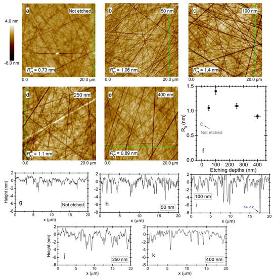
Figure 1.
AFM scans of (a) unprocessed; (b–e) plasma-etched crystals. (f) Surface roughness Rq and (g–k) cross-sectional cuts (marked in green, short-dashed line).
It is clearly seen that deeper scratches were hidden under the initial relatively smooth polished surface (Figure 1a,g). They also were present after 50 nm (Figure 1b,h) and 100 nm (Figure 1c,i) etchings. The highest increase of surface roughness up to Rq = 1.4 nm was observed for the latter case. An uneven etching of the polished crystal surface might be explained in the following way. The scratches generated by the grinding and polishing processes remained filled with a redeposited mixture of crystal nanoparticles and remnants of the polishing slurry. This redeposited material had a lower density as it was demonstrated in the case of the polishing of fused silica [26]. It was expected that the etching rate of the redeposited mixture would be higher than for a pure Co:MALO crystal, which has a high hardness (8.2 on the Mohs scale [27]). Therefore, after initial exposure to the plasma, that lower density mixture was effectively removed, and cracks were uncovered with their almost real depth. During longer etchings of 250 nm and 400 nm depth, the plasma treatment started to reveal its polishing aspect on the crystal surface. The maximum depths of scratches were reduced from 5–6 nm (Figure 1f) to 3–4 nm (Figure 1j) and 2–3 nm (Figure 1k). Correspondingly, the surface roughness decreased down to Rq = 1.1 nm and Rq = 0.89 nm, respectively. The changes of Rq with the etching depth are summarized in Figure 1f. A plasma etching of 400 nm in this case was optimal in order to maintain the initial surface quality of the polished spinel crystal. It is very likely that in this particular case, a deeper etching of ~500–600 nm would allow to reach a smooth surface, comparable to a plasma-unprocessed sample. However, this possible trend should be examined by additional investigations. The observed changes in surface roughness and topography might be different if other grinding and polishing recipes are used. This might lead to different depths and surface density of cracks, depending on the chosen polishing slurries, their fraction, number of process steps and their durations, applied forces, pH, temperature, etc. This might be illustrated by previously obtained roughness results of a very similar oxygen plasma etching of single-crystal YAG-polished substrates [28], which have comparable hardness characteristics (8.5 on the Mohs scale) as those of the Co:MALO crystal. There, a 60 nm etching resulted in Rq = 0.27 nm while the nonetched initial surface had a bigger Rq = 0.37 nm.
3.2. Transmittance
Plasma-etched samples also showed a decrease of transmittance in the 200–400 nm range, which correlated with the etching depth/time (Figure 2).
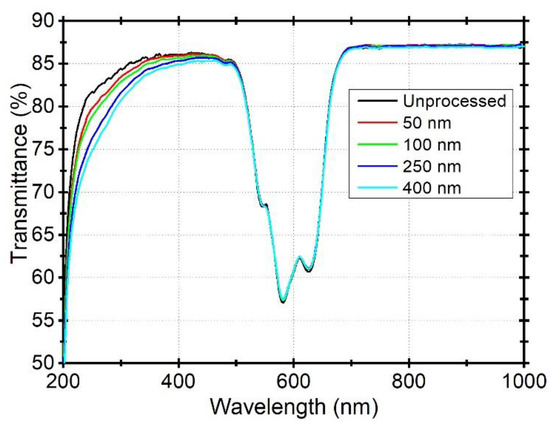
Figure 2.
Transmittance of unprocessed and different-depth plasma-etched Co2+:MgAl2O4 crystals. Absorption band at ~600 nm is due to doped Co2+ ions.
An increased optical scatter due to a higher surface roughness by the etching sample to a 100 nm depth could not exceed ~0.0012% at 300 nm (calculated using the values R0 (one surface, at 300 nm) = 0.075, σ1 = 0.73 nm, σ2 = 1.4 nm in the formula according to the diffuse reflectance and surface roughness relation in [29]). The induced additional absorption in the UV range with an increased exposure time to the plasma might be another reason; however, we cannot provide a more detailed explanation for this. One might think about a likely induced contamination by the plasma source, but multiple previous experiments with a similar etching of fused-silica substrates did not show any decrease of transmittance down to 190 nm. Possible contaminants should also reduce the laser damage resistance; however, on the contrary, the LIDT did not decrease as shown below. The decreased UV transmission also should not have any negative impact on the Q-switching properties of the Co2+:MgAl2O4 crystal, as it was concluded in a study by Denker et al. [30].
3.3. TEM Analysis
The purpose of the TEM analysis was to look for possible subsurface defects, which might be formed during polishing [31] and could decrease the LIDT of the crystals. The TEM image of mechanically polished and plasma-unprocessed crystal (Figure 3a) clearly shows a nonhomogeneous subsurface damage layer which extends horizontally through the whole TEM image and reaches a maximum depth of ~250–300 nm.
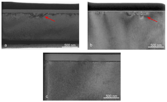
Figure 3.
TEM images of (a) plasma-unprocessed crystal, (b) plasma-etched to 100 nm and (c) plasma-etched to a 250 nm depth. The biggest accumulations of subsurface defects are marked by red arrows.
Most of these defects within smaller depths were removed after a plasma etching of 100 nm (Figure 3b), but several accumulations were still present in the ~100–300 nm depth range. Figure 3c shows a plasma-etched crystal to a 250 nm depth, which did not have any damaged subsurface. It is worth to mention that the thin dark band just beneath the surface was due to a possible curvature of FIB thinned lamella and the resulting increased scatter of the source electrons. In Figure 4a–c, the TEM images show closer views of the same samples, and Figure 4d additionally shows the plasma-etched sample to a 400 nm depth, which also did not exhibit any damaged layer.
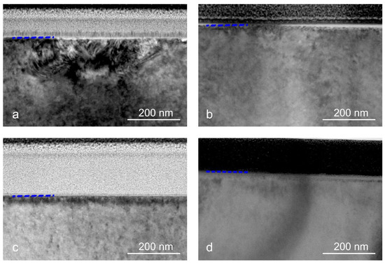
Figure 4.
TEM images of (a) plasma-unprocessed crystal, (b) plasma-etched to 100 nm, (c) plasma-etched to 250 nm and (d) plasma etched to 400 nm. The blue dotted line indicates the surface of samples.
Several studies have revealed that ion bombardment might induce the amorphization of the subsurface of a crystalline material. For example, the exposure of a Si surface for 30 s to Ar+ ions of 150 eV energies led to an amorphous subsurface layer with a thickness of 5 nm [32]. Modelling the impact of 3 × 10¹⁴ ion/cm2 Ar+ with 500 eV energy onto a Si surface demonstrated the formation of a damaged amorphous subsurface layer with a thickness of 3 nm [33]. It was also interesting to trace whether the presented oxygen plasma processing did not induce additional structural damages to the Co2+:MgAl2O4 crystal subsurface, especially for longer duration etchings to 250 nm and 400 nm depths. In Figure 5, a high-resolution TEM image and electron diffractogram (inset) show a crystalline cubic structure, which is present immediately below the surface of the plasma-unprocessed Co:MALO crystal.
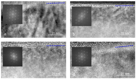
Figure 5.
High-resolution TEM images of (a) plasma-unprocessed crystal, (b) plasma-etched to 100 nm, plasma-etched to 250 nm (c) and plasma-etched to 400 nm (d). The blue dotted line indicates the surface of samples. Insets present the electron diffractogram of a selected area.
The crystallinity of the subsurface remained unchanged in all plasma-etched samples (Figure 5a–c).
3.4. Laser-Induced Damage Threshold
Surface LIDT measurement results using the R(1)-on-1 protocol at 1540 nm for 3.5 ns pulses of nonetched and oxygen-plasma-processed Co:MALO crystals are shown in Figure 6.
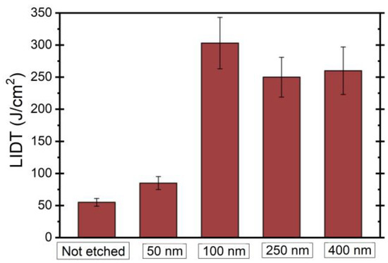
Figure 6.
Surface LIDT (R(1)-on-1) for 1064 nm (τ = 3.5 ns, d = 55 µm) of unprocessed and plasma-etched to different depths Co:MALO crystals.
An etching of 50 nm already improved by 1.5 times the initial optical resistance of the plasma-unprocessed surface (55 ± 6 J/cm2). However, a huge LIDT increase by ~5–6 times up to ~250–300 J/cm2 was manifested for deeper etchings—100, 250 and 400 nm. It would be relevant to compare these obtained values to the results of other investigations, or to the bulk LIDT values of spinel crystal. However, to the best of our knowledge, such published results do not exist. Still, we may compare the obtained trend in LIDT values while changing the etching depth with previous research on etching fused-silica substrates (though oxygen plasma ion energies and current densities were not exactly the same in that investigation, which resulted in the highest LIDT increase) [17]. A 50 nm etching of FS already resulted in a twofold increase of the LIDT at 355 nm (single-shot tests), while a 220 nm depth etching resulted in a maximum increase of the LIDT (~15× increase comparing to the nonetched FS substrate). A much more pronounced effect of the plasma etching there might be related to the fact that in general, the absorption capabilities of polishing remnants are even stronger in the UV range. However, the LIDT of FS etched to ~550 nm decreased by about two times compared with the LIDT at d = 220 nm. We did not observe a drop in the LIDT in the present research of the plasma etching of Co-doped spinel. However, when using a longer (and deeper) etching time, another damage resistance trend might occur. This might be addressed in future experiments. Kamimura et al. used a low-energy RF argon plasma etching of CsLiB6O10 (CLBO) crystals and after a 60 nm etching, they observed a 10-time increase of their lifetime for 266 nm 100 Hz laser pulses with a 90–100 MW/cm2 power density [20].
To our best knowledge, there are no other published results regarding alternative technologies for removing the damaged subsurface layer of magnesium aluminate spinel crystals.
There was no clear correlation between the subsurface damages observed by TEM and the obtained laser damage resistance of crystals at 1540 nm. Though a 100 nm etched sample did not have a continuously damaged subsurface layer like a plasma-unprocessed crystal (Figure 3a), it still had some clearly seen subsurface defects (Figure 3b). Deeper-etched crystals did not show any damaged layer (Figure 3c and Figure 4c,d), but their LIDTs were not higher.
More detailed information about the damage initiating defect densities might be obtained by fitting damage probability data, which was discussed in the work by Batavičiūtė et al. [34]. Two types of defect ensembles could be identified in our case. They had completely different LIDTs: a low LIDT (55 J/cm2 as clearly seen by fitting data for the nonetched sample (Figure 7a) and a high LIDT of 239 J/cm2 (that ensemble is already seen in the damage probability data of 50 nm etched sample (Figure 7b)).
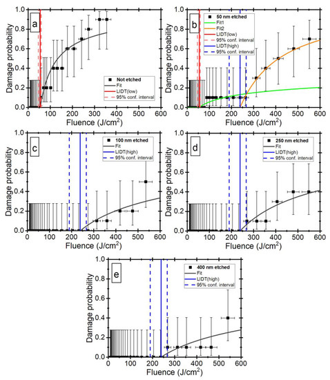
Figure 7.
Damage probabilities and fittings for the calculation of defect densities for (a) nonetched and (b–e) plasma-etched to different depths Co:MALO crystals.
Assuming that these ensembles were degenerate (all defects in the corresponding ensemble have the same LIDT), the extraction of their densities was possible by setting their corresponding LIDT values and then fitting each sample’s damage probability data. The following points are important to understand the fitting principles and assumptions which were used:
- It was assumed that low-LIDT defects were completely removed for the 250 nm etching case. Therefore, the LIDT of the other ensemble of 239 J/cm2 was obtained by fitting the 250 nm etched sample data (Figure 7d) and was used for the defect density extraction, where the “high-LIDT” defect ensemble was also already present (50 nm, 100 nm and 400 nm etched samples)
- Defect densities of the 50 nm etched sample (Figure 7b) were obtained by fitting data in two ranges separately. A low LIDT of 55 J/cm2 (marked as a red line) was used for the 0–300 J/cm2 range fitting (“Fit 1”), a high LIDT of 239 J/cm2 (marked as a blue line) was fixed for the 300–600 J/cm2 range fitting (“Fit 2”—also assuming, that damage probabilities were zero in the 0–300 J/cm2 range for this high-LIDT defect ensemble). It should be noted that here, the LIDTs of two different defect ensembles are shown, but not the LIDT of the 50 nm etched sample, which was 85 ± 11 J/cm2 (Figure 6);
- Defect densities for the 100 nm and 400 nm etched samples (Figure 7c,e) were calculated by using a LIDT value of 239 J/cm2, obtained for the 250 nm etched sample;
Figure 8 shows the cumulative defect density (sum of both ensemble densities). It is important to understand that the calculated total defect density value is just the lower limit of a possible real density, since deeper than 400 nm etchings might reveal a third ensemble of defects, whose LIDT might still be higher than 239 J/cm2. The initial defect density was reduced 10 times after the etching to 50 nm.
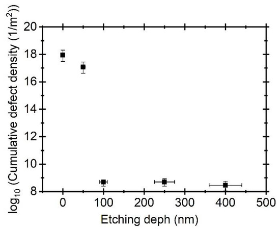
Figure 8.
Index of cumulative defect density for nonetched and plasma-etched to different depths Co:MALO crystals.
The low-LIDT defect ensemble was completely removed after the plasma etching to a 100 nm depth and the remaining high-LIDT defect density dropped to 5.012 × 10⁸/m2. It was slightly reduced after the etching of 400 nm to 3.162 × 10⁸/m2, but the difference was negligible considering the error bars. The data presented in Figure 6, Figure 7 and Figure 8 suggest that an applied low-energy oxygen plasma etching to depths ≥100 nm for the investigated spinel crystals is optimal for a huge improvement of their surface LIDT. However, it is worth to note that the optimal depth should also depend on the used chemomechanical polishing procedure and its technological steps, such as the choice of polishing compounds, their fractions, the polishing time of each step, load, temperatures, the pH of the slurries, etc.
4. Conclusions
A low-energy oxygen plasma etching of commercially polished Co2+:MgAl2O4 crystals was performed using different etching depths of 50, 100, 250 and 400 nm. Shorter plasma treatments deepened surface scratches, which increased the initial Rq = 0.73 nm to Rq = 1.4 nm for the 100 nm etching case. However, deeper plasma etchings resulted in much smoother surfaces with Rq = 0.84 nm, which was almost equal to the initial value. TEM images of nonetched crystal showed a continuous damaged subsurface layer, having extended defect agglomerations down to a depth of 250–300 nm. These damages were completely removed in the 250 nm and 400 nm etching cases. All performed plasma treatments did not made any changes to the initial crystalline structure below the surface. The R(1)-on-1 laser-induced damage threshold for 1540 nm 3.5 ns laser pulses was 55 ± 6 J/cm2 for the plasma-unprocessed crystal surface. A substantial LIDT improvement up to 303 ± 40 J/cm2 was obtained after 100 nm removal by plasma. The laser radiation resistance did not change within the error bars for deeper etchings of 250 nm and 400 nm. The damage probability curves demonstrated two types of defects with corresponding low and high LIDTs. The extracted defect densities by fitting damage probability data allowed the calculation of an initial total defect density of 1018/m2, which dropped to 5.012 × 10⁸/m2 after 100 nm of removal by plasma. A plasma etching of 400 nm was optimal for a huge increase of the LIDT, the removal of subsurface damage and for almost preserving the initial surface quality and roughness. The presented results demonstrate a good potential of oxygen plasma etching for obtaining highly laser-damage-resistant Co2+:MgAl2O4 crystals for high-power laser applications.
Author Contributions
G.A.: conceptualization, supervision, project administration, resources, methodology, validations, formal analysis, investigation, writing—original draft, review and editing, funding acquisition. M.S.: formal analysis, methodology, investigation, visualization, writing—review and editing. R.J.: methodology, validation, formal analysis, investigation, writing—review and editing. All authors have read and agreed to the published version of the manuscript.
Funding
This research has received funding from European Social Fund (project no. 09.3.3-LMT-K-712-19-0180) under a grant agreement with the Research Council of Lithuania (LMTLT).
Institutional Review Board Statement
Not applicable.
Informed Consent Statement
Not applicable.
Data Availability Statement
The data presented in this study are available on reasonable request from the corresponding author.
Acknowledgments
We are grateful to Lina Volosevičienė for her assistance with the AFM measurements and sample preparation, Algirdas Selskis for the TEM specimen preparation using FIB milling and Andrius Melninkaitis for supporting the LIDT data interpretation.
Conflicts of Interest
The authors declare no conflict of interest.
References
- Mlynczak, J.; Belghachem, N. High peak power generation in thermally bonded Er3+, Yb3+: Glass/Co2+: MgAl2O3 microchip laser for telemetry application. Laser Phys. Lett. 2015, 12, 045803. [Google Scholar] [CrossRef]
- van As, G. Erbium lasers in dentistry. Dent. Clin. 2004, 48, 1017–1059. [Google Scholar] [CrossRef]
- Lutzmann, P.; Frank, R.; Hebel, M.; Ebert, R. Potential of Remote Laser Vibration Sensing for Military Applications; Forschungsinstitut Fuer Optronik und Mustererkennung Gutleuthausstrasse (DE): Ettlingen, Germany, 2005. [Google Scholar]
- Qi, Y.; Bai, Z.; Wang, Y.; Zhang, X.; Qi, Y.; Ding, J.; Bai, Z.; Lu, Z. Research progress of all-solid-state passively Q-switched Er:Yb:glass lasers. Infrared Phys. Technol. 2021, 116, 103727. [Google Scholar] [CrossRef]
- Siegman, A.E. Laser Q-Switching. In Lasers; University Science Books: Sausalito, CA, USA, 1986. [Google Scholar]
- Kozlowski, M.R.; Carr, J.; Hutcheon, I.D.; Torres, R.A.; Sheehan, L.M.; Camp, D.W.; Yan, M. Depth profiling of polishing-induced contamination on fused silica surfaces. In Proceedings of the Laser-Induced Damage in Optical Materials, Boulder, CO, USA, 6–8 October 1997; Volume 3244, p. 11. [Google Scholar] [CrossRef]
- Suratwala, T.; Steele, W.; Wong, L.; Feit, M.D.; Miller, P.E.; Dylla-Spears, R.; Shen, N.; Desjardin, R. Chemistry and formation of the Beilby layer during polishing of fused silica glass. J. Am. Ceram. Soc. 2015, 98, 2395–2402. [Google Scholar] [CrossRef]
- Menapace, J.A.; Penetrante, B.; Golini, D.; Slomba, A.F.; Miller, P.E.; Parham, T.G.; Nichols, M.; Peterson, J. Combined advanced finishing and UV-laser conditioning for producing UV-damage-resistant fused-silica optics. In Proceedings of the Boulder Damage, 3–5 June 2002; p. 13. [Google Scholar] [CrossRef]
- Salo, V.; Atroschenko, L.; Garnov, S.; Khodeyeva, N. Structure, impurity composition, and laser damage threshold of the subsurface layers in KDP and KD*P single crystals. In Proceedings of the Laser-Induced Damage in Optical Materials, Boulder, CO, USA, 30 October–1 November 1995; Volume 2714. [Google Scholar] [CrossRef]
- Vlasov, A.; Rez, J.; Fil’chenkov, M. Beilby layers on crystal surfaces. Cryst. Res. Technol. 1988, 23, 1093–1100. [Google Scholar] [CrossRef]
- Yao, C.; Shen, W.; Hu, X.; Hu, C. Evaluation of the surface and subsurface evolution of single-crystal yttrium aluminum garnet during polishing. Appl. Surf. Sci. 2023, 608, 155219. [Google Scholar] [CrossRef]
- Luo, H.; Ajmal, K.M.; Liu, W.; Yamamura, K.; Deng, H. Atomic-scale and damage-free polishing of single crystal diamond enhanced by atmospheric pressure inductively coupled plasma. Carbon 2021, 182, 175–184. [Google Scholar] [CrossRef]
- Kamimura, T.; Akamatsu, S.; Yamamoto, M.; Yamato, I.; Shiba, H.; Motokoshi, S.; Sakamoto, T.; Jitsuno, T.; Okamoto, T.; Yoshida, K. Enhancement of surface-damage resistance by removing subsurface damage in fused silica. In Proceedings of the XXXV Annual Symposium on Optical Materials for High Power Lasers: Boulder Damage Symposium, Boulder, CO, USA, 22–24 September 2004; Volume 5273, p. 6. [Google Scholar] [CrossRef]
- Pfiffer, M.; Cormont, P.; Fargin, E.; Bousquet, B.; Dussauze, M.; Lambert, S.; Neauport, J. Effects of deep wet etching in HF/HNO3 and KOH solutions on the laser damage resistance and surface quality of fused silica optics at 351 nm. Opt. Express 2017, 25, 4607–4620. [Google Scholar] [CrossRef]
- Brusasco, R.M.; Penetrante, B.M.; Peterson, J.E.; Maricle, S.M.; Menapace, J.A. UV-laser conditioning for reduction of 351-nm damage initiation in fused silica. In Proceedings of the Boulder Damage, Boulder, CO, USA, 1–3 October 2002; Volume 4679, p. 8. [Google Scholar] [CrossRef]
- Juškevičius, K.; Buzelis, R.; Abromavičius, G.; Samuilovas, R.; Abbas, S.; Belosludtsev, A.; Drazdys, R.; Kičas, S. Argon plasma etching of fused silica substrates for manufacturing high laser damage resistance optical interference coatings. Opt. Mater. Express 2017, 7, 3598–3607. [Google Scholar] [CrossRef]
- Abromavičius, G.; Juodagalvis, T.; Buzelis, R.; Juškevičius, K.; Drazdys, R.; Kičas, S. Oxygen plasma etching of fused silica substrates for high power laser optics. Appl. Surf. Sci. 2018, 453, 477–481. [Google Scholar] [CrossRef]
- Shao, T.; Sun, L.; Li, W.; Zhou, X.; Wang, F.; Huang, J.; Ye, X.; Yang, L.; Zheng, W. Understanding the role of fluorine-containing plasma on optical properties of fused silica optics during the combined process of RIE and DCE. Opt. Express 2019, 27, 23307–23320. [Google Scholar] [CrossRef] [PubMed]
- Kamimura, T.; Nakai, K.; Mori, Y.; Sasaki, T.; Yoshida, H.; Nakatuka, M.; Tanaka, M.; Toda, S.; Tanaka, M.; Yoshida, K. Improvement of laser-induced surface damage in UV optics by ion beam etching (CsLiB6O10 and fused silica). In Proceedings of the Laser-Induced Damage in Optical Materials, Boulder, CO, USA, 28 September–1 October 1998; Volume 3578, pp. 695–701. [Google Scholar] [CrossRef]
- Kamimura, T.; Yoshimura, M.; Mori, Y.; Sasaki, T.; Yoshida, K. Effect of RF Plasma Etching on Surface Damage in CsLiB6O10 Crystal. Jpn. J. Appl. Phys. 1999, 38, L181–L183. [Google Scholar] [CrossRef]
- Kubart, T.; Nyberg, T.; Berg, S. Modelling of low energy ion sputtering from oxide surfaces. J. Phys. D Appl. Phys. 2010, 43, 205204. [Google Scholar] [CrossRef]
- Yumashev, K.; Denisov, I.; Posnov, N.; Prokoshin, P.; Mikhailov, V. Nonlinear absorption properties of Co2+:MgAl2O4 crystal. Appl. Phys. B 2000, 70, 179–184. [Google Scholar] [CrossRef]
- Papernov, S.; Brunsman, M.D.; Oliver, J.B.; Hoffman, B.N.; Kozlov, A.A.; Demos, S.G.; Shvydky, A.; Cavalcante, F.H.M.; Yang, L.; Menoni, C.S.; et al. Optical properties of oxygen vacancies in HfO2 thin films studied by absorption and luminescence spectroscopy. Opt. Express 2018, 26, 17608–17623. [Google Scholar] [CrossRef]
- Xu, C.; Yi, P.; Fan, H.; Qi, J.; Qiang, Y.; Liu, J.; Tao, C.; Li, D. Correlations between the oxygen deficiency and the laser damage resistance of different oxide films. Appl. Surf. Sci. 2014, 289, 141–144. [Google Scholar] [CrossRef]
- Panahibakhsh, S.; Jelvani, S.; Maleki, M.H.; Mollabashi, M.; Jaberi, M. Increasing the laser damage threshold of the Nd:YAG crystal by ArF laser irradiation. Eur. Phys. J. Plus 2014, 129, 37. [Google Scholar] [CrossRef]
- Liao, D.; Chen, X.; Tang, C.; Xie, R.; Zhang, Z. Characteristics of hydrolyzed layer and contamination on fused silica induced during polishing. Ceram. Int. 2014, 40, 4479–4483. [Google Scholar] [CrossRef]
- Available online: https://www.meta-laser.com/q-switch-crystals/co-spinel-q-switch-crystals.html (accessed on 22 December 2022).
- Abromavičius, G.; Kyžas, N.; Belosludtsev, A. Oxygen plasma etching of YAG crystals. In Proceedings of the SPIE Optical Systems Design, Frankfurt, Germany, 14–17 May 2018; Volume 10691. [Google Scholar] [CrossRef]
- Bennett, H.E.; Porteus, J.O. Relation Between Surface Roughness and Specular Reflectance at Normal Incidence. J. Opt. Soc. Am. 1961, 51, 123–129. [Google Scholar] [CrossRef]
- Denker, B.; Galagan, B.; Osiko, V.; Sverchkov, S.; Karlsson, G.; Laurell, F. Comparison of cobalt-activated spinel crystals grown by various methods as saturable absorbers for 1.3–1.6 μm lasers. In Proceedings of the Advanced Solid-State Photonics, San Antonio, TX, USA, 2–5 February 2003; Volume 83, p. 216. [Google Scholar] [CrossRef]
- Namba, Y.; Ohnishi, N.; Yoshida, S.; Harada, K.; Yoshida, K.; Matsuo, T. Ultra-precision float polishing of calcium fluoride single crystals for deep ultra violet applications. CIRP Ann. 2004, 53, 459–462. [Google Scholar] [CrossRef]
- Matsuda, A.; Nakakubo, Y.; Takao, Y.; Eriguchi, K.; Ono, K. Advanced Contactless Analysis of Plasma-Induced Damage on Si by Temperature-Controlled Photoreflectance Spectroscopy. Jpn. J. Appl. Phys. 2011, 50, 08KD03. [Google Scholar] [CrossRef]
- Moore, M.C.; Kalyanasundaram, N.; Freund, J.B.; Johnson, H.T. Structural and sputtering effects of medium energy ion bombardment of silicon. Nucl. Instrum. Methods Phys. Res. Sect. B Beam Interact. Mater. At. 2004, 225, 241–255. [Google Scholar] [CrossRef]
- Batavičiutė, G.; Grigas, P.; Smalakys, L.; Melninkaitis, A. Revision of laser-induced damage threshold evaluation from damage probability data. Rev. Sci. Instrum. 2013, 84, 045108. [Google Scholar] [CrossRef] [PubMed]
Disclaimer/Publisher’s Note: The statements, opinions and data contained in all publications are solely those of the individual author(s) and contributor(s) and not of MDPI and/or the editor(s). MDPI and/or the editor(s) disclaim responsibility for any injury to people or property resulting from any ideas, methods, instructions or products referred to in the content. |
© 2023 by the authors. Licensee MDPI, Basel, Switzerland. This article is an open access article distributed under the terms and conditions of the Creative Commons Attribution (CC BY) license (https://creativecommons.org/licenses/by/4.0/).