Abstract
This study investigated the electro-optic properties of organic light-emitting diode (OLED) devices with the addition of an interlayer. A device with the perfluorododecyl-1H,1H,2H,2H-triethoxysilane–perfluorotetradecyl 1H,1H,2H,2H-triethoxysilane mixture (hybrid solution) membrane applied to the hole injection layer (HIL) using a self-assembled monolayer (SAM), along with N,N’-Bis (naphtha-len-1-yl)-N,N’-bis(phenyl)-2,2’-dimethylbenzidine (α-NPD) applied to the hole transport layer (HTL), was fabricated and subsequently assessed. Compared to the device without an HIL, the device with HIL using SAM showed a luminance of 1630.16 (Cd/m2) at the maximum cut-off voltage of 11 V, and the efficiency was increased to ≥200% from the initial turn-on voltage of 3 V to the maximum cut-off voltage. These results suggest that adding an interlayer and the consequent carrier ladder effect led to more efficient injection and transport, possibly lowering the hole injection barrier and allowing excellent power efficiency.
1. Introduction
Organic light-emitting diodes (OLEDs) are light-emitting devices subject to ongoing research. They are structured in several layers of organic materials. When an electric field is applied to the cathode, light is emitted as the electrons generated at each pole meet the holes [1]. Except for special cases, OLED devices have an inherent ability to emit light even on the surface of materials given the presence of thin films of such structures, thus allowing the production of more flexible designs compared to conventional light-emitting devices, with a multitude of advantages, ranging from higher color expression to wider viewing angles than conventional devices [2]. Current OLED displays consist of a hole injection layer (HIL), hole transport layer (HTL), emissive layer (EML), electron transport layer (ETL), and electron injection layer (EIL), as well as a layer that assists in the efficient transport of holes and electrons via the addition of an interlayer and a layer in which the electrons and holes meet to produce light emission [3]. Self-emitting organic materials emit light upon application of electricity based on “electroluminescence”. The excitation state is temporarily unstable and the return to the ‘ground state’ is immediate, since electrons seek to find a stable state. As electrons return from the excited state to the ground state, the energy level decreases back to the original level, when the reduced energy is emitted in the form of light.
The most-applied material used as the anode in the fabrication of OLED devices at present is indium tin oxide (ITO) on a glass substrate for transparent electrodes [4]. ITO is a type of transparent conducting oxide material composed of indium oxide (In2O3) and tin oxide (SnO2). ITO is widely used in the fabrication of displays, electronic paper, OLED, architecture, solar cells, and protective coatings due to its electrical conductivity, optical transparency, excellent substrate adhesion, high-temperature resistance, ability to form thin films, and chemical resistance to moisture [5].
Tang et al. reported the HTL of an OLED device could be modified to improve performance by reducing the driving voltage, which was the first work to modify the device’s interlayer. Tang et al. achieved quantum efficiency (1% photon/electron), luminance efficiency (1.5 lm/W), and brightness (>1000 cd/m2) at driving voltages less than 10 volts in 1987 [6]. Additionally, the light emitting layer was doped with other substances in 1989, which increased efficiency by more than two fold compared to the previous work done at driving voltages less than 10 volts [7]. Significant improvement in electron injection was achieved by introducing a thin LiF film and reducing the electronic barrier of the organic/AI interface layer, further improving the efficiency of the device [8]. In recent years, there has been intensive research into the modification of the inner layer of the device, aiming to create high-brightness, high-efficiency, low-power, and commercial technologies.
The most well-known studies on the HIL layer involve using materials such as PEDOT:PSS, 2-TNATA, MoOx [9,10] and SAM, while those on the HTL layer report on the use of TCTA, TPD, and m-MTDATA [11]. The two layers act to improve the efficiency of hole injection to the subsequent layer by increasing the highest occupied molecular orbital (HOMO) level [12].
Self-assembled monolayers (SAMs) are organic monolayers with an intrinsic nanostructure that are formed at phase boundaries [13]. They are advantageous in inducing a change in the substrate, as the SAM film coating on the surface of an existing solid material may provide lubrication or prevent oxidation [14]. Based on these characteristics, SAMs have been actively and continuously studied since their first introduction by Bigelow and Zisman in 1946 [15]. The structure of SAMs has a head group that can bind to the surface of a solid material, an alkyl chain at the center of the molecular structure, and a functional group with a final role in the molecular membrane. The film is formed through hydrolysis and polymerization involving the head group on a solid surface [16]. In recent years, research has focused on the improvement of the performance of OLEDs using SAM [17,18,19,20]. Fluorinated organic compounds are widely used for improving the efficiency of organic light-emitting devices owing to fluorine exhibiting a large electric dipole moment [21]. Additionally, in the field of medical devices and research, significant work has been done in recent years to develop OLED systems based on ITO and improve luminance and its impact on the human body and health [22]. The healing phenomenon occurs at the sites via a photobiological reaction depending on the depth through the human body in the spectrum between 300 nm and 830 nm [23]. An OLED device in photomedicine is engaged during mitochondrial ATP production at specific wavelength bands of PBM. This method is applied in the fields of biological and medical sciences for wound healing and the reduction of pain and inflammation, among other applications. Such methods are increasingly being used in LED and laser treatments, and recently, a PBM therapy using OLED-based flexible materials has been widely utilized [24,25]. Long-term use is essential to obtain the PBM effect in optimal conditions [26].
Recent studies have reported varying effects of OLED-based PBM therapy on the human body and cells of different types according to the generated wavelength bands. Beneficial effects are produced as melanin or nitric oxide (NO) levels that affect the human body are increased or decreased at the given wavelength bands. However, using a photomedical device requires a target site to be irradiated for a long period of time. Because of the short lifetime of the optical device, its application is limited [27]. Therefore, more studies on increasing the efficiency of OLED should be conducted, which could offer features such as long-time use and portability [28]. In addition, more studies should be conducted on methods to increase the efficiency of OLED long-time use with portability [28].
2. Materials and Methods
2.1. Materials
For the ITO at the anode, a product of AMG Co., Ltd. (Seoul, Republic of Korea) was used. The ITO was deposited at a 150 ± 10 nm thickness at ≤10 Ω/sq sheet resistance and ≥85% λ = 550 nm transmission. For the SAMs, the perfluorododecyl-1H,1H,2H,2H-triethoxysilane-perfluorotetradecyl 1H,1H,2H,2H-triethoxysilane mixture (hybrid solution) was purchased from Gelest (Bucks County, PA, USA).
2.2. Cleaning Process
The ITO substrate was washed by applying acetone, deionized (DI) water, and isopropyl alcohol (IPA), and following the hot plate drying, SAMs were produced through solution deposition, with the device fabricated through the deposition of each layer using a vacuum thermal evaporator.
2.3. SAMs and Device Deposition Process
In the deposition of each type of SAM to the surface of the ITO substrate, the following procedures were performed. Taking the washed ITO in a 500 mL beaker, a 5 mM hybrid solution was mixed with ethanol for 1 h to produce the solution, and the ITO substrate was placed in the solution for 1 h for filming. In the comparative analysis of the filming by time, the washed ITO substrate was placed in a 5 mL PFA container with the hybrid solution and a 500 mL PFA container simultaneously to mediate vapor deposition, after which the ITO substrate was washed with IPA. Following hot plate drying, the substrate properties were analyzed based on the contact angle, while the performance characteristics were comparatively analyzed by fabricating N,N’-Bis(naphthalen-1-yl)-N,N’-bis(phenyl)-2,2’-dimethylbenzidine(α-NPD) (50 nm), Alq3 (50 nm), LiF (0.6 nm), and Al (100 nm) devices using the vacuum thermal evaporator and the ITO substrate with the SAM film coating. The molecular structure of SAMs consists of a head group that chemically adheres to the substrate, a central alkyl chain that allows a regular pattern of molecular film formation, and a functional group that affects the function of the molecular film [14]. A hybrid solution was used as the SAM material; α-NPD was used for the HTL. Next, using a vacuum thermal evaporator, three devices were fabricated: one with an HIL and an HTL, one with only an HTL, and one with neither an HIL nor HTL. Figure 1 shows schematics of the materials used in this study as energy bands. The hole injection barrier is high due to the basic ITO work function of 4.8 eV and HOMO level of 5.5 eV to induce a difference in the hole injection barrier between HIL and HTL so that the hole carrier transport is not efficient [29,30,31,32]. In SAM filming, the perfluorododecyl-1H,1H,2H,2H-triethoxysilane–perfluorotetradecyl 1H,1H,2H,2H-triethoxysilane mixture (hybrid solution) exhibits a level of at least 5.6 eV at F10SAM [33,34] and F12SAM [34]. Table 1 describes the fabricated OLED device thickness in Device (A) with the HIL (hybrid solution) and HTL (α-NPD) composing an interlayer; Device (B) without HIL; and Device (C) without either. The goal was to ensure that the hole carrier transport is efficient via the sequential lining up of HOMO levels through the role of the interlayer.

Figure 1.
Energy band schematic.

Table 1.
OLED layer thickness.
2.4. Experimental Section
The current density–voltage–luminescence (JVL) parameters and water contact angle were measured using a McScience Inc. M3000 OLED Parameter TEST System (Republic of Korea) and an S.E.O. Co., Ltd. Peonix 300 analyzer (Republic of Korea), respectively.
3. Results and Discussion
The hydrolysis reaction starts when a film of SAM is deposited on the surface of ITO, and it is formed by the impact of Van Der Waals force. The SAM thin film deposition process on ITO varies depending on the deposition method. The dipping method might require ranging from a few minutes to many days to deposit SAM [16].
The formation of SAM on the ITO surface involves the following steps: 1. The pre-cleaned ITO is added to a solution containing SAM. The dissolved SAMs are deposited on the surface of the ITO through chemisorption. 2. The C2H5O radical of the SAM head group is replaced by the OH group under the influence of the hydrolysis process, resulting in the release of ethanol. 3. The precleaned ITO-coated glass is added to the hybrid solution. The dissolved perfluoroalkylesilanes are deposited on the surface of the ITO through chemisorption. The process of formation of monolayers has the unique feature of self-ordering due to Van der Waals forces [33].
Figure 2 shows the graph of surface energy and contact angle. Vapor deposition was used to identify the surface properties of SAMs according to the filming time. A PFA container with the hybrid solution was placed in a convection oven at 120 °C for 60 min. The result confirmed that the coating of the hydrophobic SAM film was adequate, as the hydrophobicity of the surface gradually increased. The surface initially showed a level of hydrophilicity similar to that of the basic ITO due to the low level of SAM filming of 48.68° at 1 min; however, over time, the level increased to 67.43° at 10 min, 71.78° at 30 min, and 81.26° at 60 min. When the surface energy was calculated using the Girifalco-Good-Fowkes-Young method with DI water as the reference solution, the ITO surface energy with SAM filming was found to decrease by as much as 50% from 61.93 (mN/m) at 1 min to 43.02 (mN/m) at 10 min, 38.71 (mN/m) at 30 min, and 29.81 (mN/m) at 60 min, while an inverse correlation was observed between surface energy and contact angle. This result indicated that, with the hybrid solution, the contact angle steadily increased in line with the filming time, and the longer the filming time, the higher the gradual hydrophobicity acquired by the ITO substrate. Finally, compared to the ITO substrate with its initial hydrophilicity, the film coating was found to be adequate. The surface energy can be improved by reducing the concentration of the hydroxyl groups on the ITO surface, which prevents the isolation of the hole transport layer from the ITO [21,35]. The addition of the hole injection and hole transport layers to the opto-electronic device may have improved the stability, thereby enhancing the applications potential [36]. When the surface of the substrate on which the SAM single molecular film is formed is confirmed, the effect is relatively low compared to the average surface roughness of the existing ITO [37]. The interfacial interaction between the layers can be improved by improving the surface roughness [38]. With an uneven surface, the interfacial interaction between the layers is frequently weak all through deposition [39].
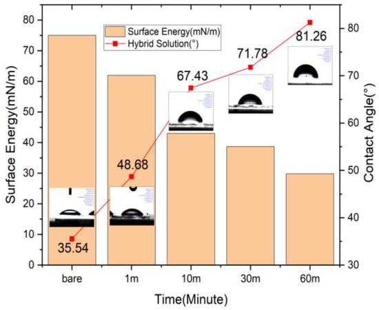
Figure 2.
Hybrid solution–surface energy and contact angle.
Figure 3 shows the characteristics of voltage and current density curves. As can be seen, the current density of the device with the injection of the hybrid solution at the HIL (Device (A)) is 3.2691 (mA/cm2) from 4 V, showing a steady increase compared to Device (B) or (C) without the HIL and HTL interlayer. Device (B) without HIL reached a current density of 4.0121 (mA/cm2), close to that of Device (A) at 6 V. Device (C) without either HIL or HTL reached the current density of 3.7802 (mA/cm2) close to that of Device (A) at 4 V, only after 7 V. These results indicated that, at the ITO work function of 4.8 eV, the 5.8 eV injection barrier up to the light emitting layer (Alq3) could be improved by the HIL with SAM filming as the energy gap in HOMO level could be reduced with respect to the 5.5 eV HTL (α-NPD). The improved hole injection barrier could reduce the driving voltage at the same current density, suggesting that a high level of current per unit area was allowed to flow in line with the increase in driving voltage.
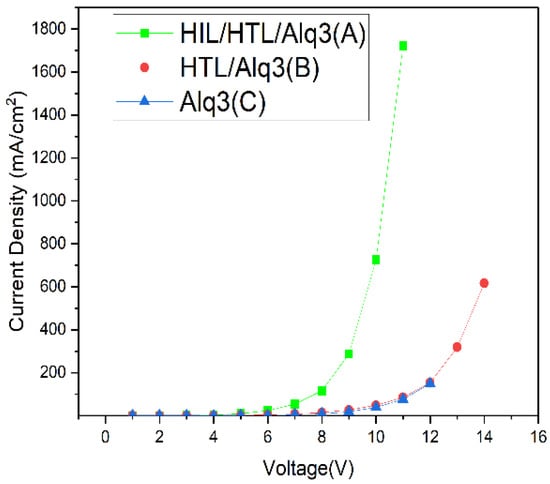
Figure 3.
The curves of current density and voltage characteristics with linear–linear scale.
Figure 4 shows the characteristics of the voltage and luminance curves. The turn-on voltage of device A is ~2–3 V (0.12 Cd/m2), which is higher than that of devices B and C. It was observed that by adding the interlayer of HTL and HIL, the device turn-on voltage can be reduced by 2–3-fold. However, device C can take a small numerical value at the corresponding voltage. The difference did not decrease, indicating a clear difference between (A) 1630.16 (Cd/m2) at the operating voltage of 11 V compared to (B) 97.63 (Cd/m2) applied at the same voltage. Figure 3 and Figure 4 show that the role of the hole transport is important, further emphasizing the necessity of the hole-injection and hole-transporting layers for improving the luminance and current density of the electro-optic device.
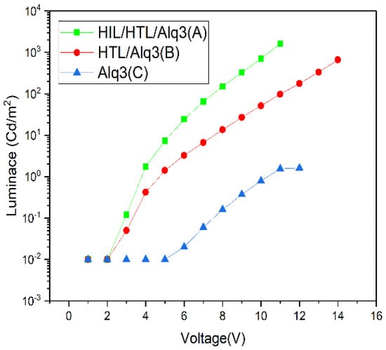
Figure 4.
The curves of luminance and voltage characteristics with log-linear scale.
Figure 5 shows the characteristics of the L-J curves. As can be seen, the difference in luminance between Device (A) and Device (B), which acquire a similar level of high current density against low voltage, was as high as 200%: 704.54 (Cd/m2) for (A) and 333.72 (Cd/m2) for (B) at 300 ± 20 (mA/cm2). The maximum luminance was 1630.16 (Cd/m2) for (A), 661.37 (Cd/m2) for (B), and 1.61 (Cd/m2) for (C), confirming the high performance of (A) with the highest luminance. Meanwhile, the luminance was markedly low across all parts for (C) with neither HIL nor HTL. In addition, compared to (B) and (C), the luminance was significantly higher for (A) at the same voltage and current density levels, attributed to efficient hole injection based on HIL and the subsequent transport through HTL in (A), leading to higher driving voltage and higher current density at the same voltage.
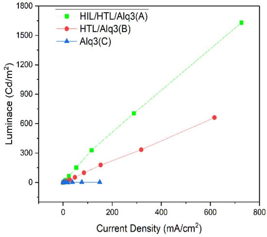
Figure 5.
The curves of luminance and current density characteristics with linear–linear scale.
Figure 6 and Figure 7 show the characteristics of the Power Eff-V and Eff-J curves. Based on the power efficiency and the current efficiency of the device, Device (A) showed at least 50% higher power efficiency performance than Device (B) or (C) at the same voltage: 0.06407 (lm/W) at the maximum emission voltage of 11 V, as Figure 5 shows. In addition, as Figure 6 shows, Device (A) showed a current efficiency performance of 0.2245 (Cd/A) at the highest current density of 704.54 (Cd/m2). The efficiency exhibited by Device (A) was markedly high in comparison to Device (C) at 0.0020527 (Cd/A). The results of this study suggest that through the role of SAMs acting as the HIL and of the HTL, the hole injection barrier between organic films was reduced to allow a greater level of current to flow per unit area.
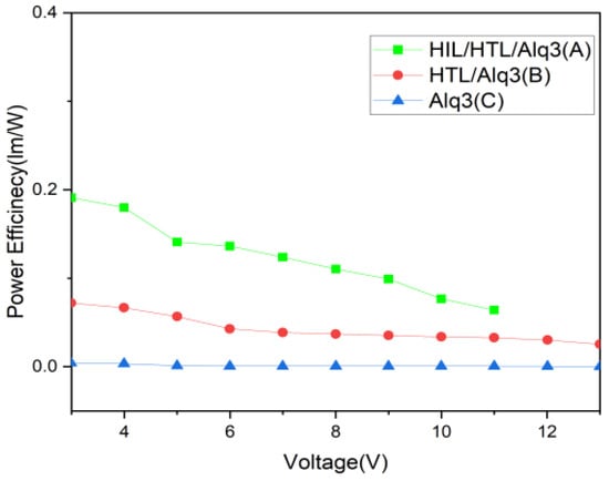
Figure 6.
The curves of Power efficiency and Voltage characteristics with linear–linear scale.
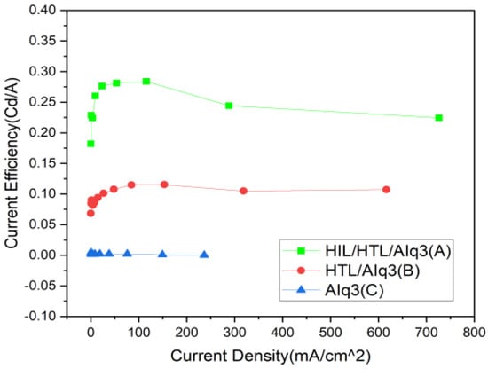
Figure 7.
The curves of current efficiency and current density characteristics with linear–linear scale.
4. Conclusions
This study investigated the electro-optic properties of an OLED device with the addition of an interlayer. The difference according to the interlayer addition was clear. At the initial 3 V, Device (A) showed at least 200% efficiency at 0.12 (Cd/m2) luminance compared to Device (B) at 0.5 (Cd/m2). At the maximum emission of 11 V, the level of luminance was markedly higher for (A) at 1630.16 (Cd/m2) than (B) at 97.63 (Cd/m2) at the same voltage. In addition, the SAMs effectively reduced the hole injection barrier between organic films in each constituting layer of the OLED, which led to a higher current density of 1722 (mA/cm2) for (A) compared to the 84.955 (mA/cm2) for (B). As such, the device with the interlayer via SAM filming could reduce the work function between the basic ITO (4.8 eV) and light-emitting layer Alq3 (5.8 eV) to exert a carrier ladder effect and allow efficient hole carrier transport, which was shown to cause a low driving voltage and higher power efficiency and current density at the same voltage. In summary, the findings of this study suggest that an increase in OLED efficiency could lead to an increase in the performance of photobiomedical devices.
Author Contributions
Conceptualization, S.-G.P.; methodology S.-G.P. and S.-S.Y.; validation, S.-G.P.; formal analysis, A.B.; investigation, S.-G.L.; resources, A.B.; data curation, S.-G.L.; writing—original draft preparation, S.-G.L.; writing—review and editing, S.-G.P. and S.-S.Y.; visualization, S.-G.L.; supervision, S.-G.P.; project administration, S.-G.P. All authors have read and agreed to the published version of the manuscript.
Funding
This research is funded by the Financial Program for Customized Research Capabilities in 2022.
Institutional Review Board Statement
Not applicable.
Informed Consent Statement
Not applicable.
Data Availability Statement
The data presented in this study are available on request from the corresponding author.
Conflicts of Interest
The authors declare no conflict of interest.
References
- Jou, J.-H.; Kumar, S.; Agrawal, A.; Li, T.-H.; Sahoo, S. Approaches for fabricating high efficiency organic light emitting diodes. J. Mol. Cell. Cardiol. 2015, 3, 2974–3002. [Google Scholar]
- Tyan, Y.-S. Organic light-emitting-diode lighting overview. J. Photon. Energy 2011, 1, 011009. [Google Scholar] [CrossRef]
- Geffroy, B.; Le Roy, P.; Prat, C. Organic light-emitting diode (OLED) technology: Materials, devices and display technologies. Polymer Int. 2006, 55, 572–582. [Google Scholar] [CrossRef]
- Kim, H.; Pique, A.; Horwitz, J.S.; Mattoussi, H.; Murata, H.; Kafafi, Z.H.; Chrisey, D.B. Indium tin oxide thin films for organic light-emitting devices. Appl. Phys. Lett. 1999, 74, 3444–3446. [Google Scholar] [CrossRef]
- Tak, Y.H.; Kim, K.B.; Park, H.G.; Lee, K.H.; Lee, J.R. Criteria for ITO (indium–tin-oxide) thin film as the bottom electrode of an organic light emitting diode. Thin Solid Film. 2002, 411, 12–16. [Google Scholar] [CrossRef]
- Tang, C.W.; VanSlyke, S.A. Organic electroluminescent diodes. Appl. Phys. Lett. 1987, 51, 913–915. [Google Scholar] [CrossRef]
- Tang, C.W.; VanSlyke, S.A.; Chen, C.H. Electroluminescence of doped organic thin films. J. Appl. Phys. 1989, 65, 3610–3616. [Google Scholar] [CrossRef]
- Hung, L.S.; Tang, C.W.; Mason, M.G. Enhanced electron injection in organic electroluminescence devices using an Al/LiF electrode. Appl. Phys. Lett. 1997, 70, 152–154. [Google Scholar] [CrossRef]
- Lim, J.; Park, J.; Jhon, M.; Yeom, G. Study of the Electronic Structure of the Interfaces between 2-TNATA and MoO x. J. Nanotechnol. 2013, 13, 8025–8031. [Google Scholar]
- Su, S.-H.; Hou, C.-C.; Tsai, J.-S.; Yokoyama, M. Enhancement of efficiency of white organic light-emitting diodes with p-type hole injection layer. Thin Solid Films 2009, 517, 5293–5297. [Google Scholar] [CrossRef]
- Swayamprabha, S.S.; Nagar, M.R.; Yadav, R.A.K.; Gull, S.; Dubey, D.K.; Jou, J.-H. Hole-transporting materials for organic light-emitting diodes: An overview. J. Mater. Chem. C 2019, 7, 7144–7158. [Google Scholar]
- Yadav, R.A.K.; Dubey, D.K.; Chen, S.-Z.; Liang, T.-W.; Jou, J.-H. Role of molecular orbital energy levels in OLED performance. Sci. Rep. 2020, 10, 102317079. [Google Scholar] [CrossRef] [PubMed]
- Ulman, A. Formation and structure of self-assembled monolayers. Chem. Rev. 1996, 96, 1533–1554. [Google Scholar] [CrossRef] [PubMed]
- Chi, Y.S.; Kang, S.M.; Choi, I.S. Surface Engineering Based on Self-Assembled Monolayers. Polym. Sci. Technol. 2006, 17, 172–181. [Google Scholar]
- Bigelow, W.; Pickett, D.; Zisman, W. Oleophobic monolayers: I. Films adsorbed from solution in non-polar liquids. J. Colloid Sci. 1946, 1, 513–538. [Google Scholar] [CrossRef]
- Oh, S.-Y.; Yun, Y.-J.; Kim, D.-Y.; Han, S.-H. Formation of a self-assembled monolayer of diaminododecane and a heteropolyacid monolayer on the ITO surface. Langmuir 1999, 15, 4690–4692. [Google Scholar] [CrossRef]
- Lee, J.; Jung, B.-J.; Lee, J.-I.; Chu, H.Y.; Do, L.-M.; Shim, H.-K. Modification of an ITO anode with a hole-transporting Sam for improved OLED device characteristics. J. Mater. Chem. 2002, 12, 3494–3498. [Google Scholar] [CrossRef]
- Can, M.; Havare, A.K.; Aydın, H.; Yagmurcukardes, N.; Demic, S.; Icli, S.; Okur, S. Electrical properties of SAM-modified ITO surface using aromatic small molecules with double bond carboxylic acid groups for OLED applications. Appl. Surf. Sci. 2014, 314, 1082–1086. [Google Scholar] [CrossRef]
- An, D.; Liu, H.; Wang, S.; Li, X. Modification of ito anodes with self-assembled monolayers for enhancing hole injection in oleds. Appl. Phys. Lett. 2019, 114, 153301. [Google Scholar] [CrossRef]
- Havare, A.K. Effect of the interface improved by self-assembled aromatic organic semiconductor molecules on performance of OLED. ECS J. Solid State Sci. Technol. 2020, 9, 041007. [Google Scholar] [CrossRef]
- Zheng, H.; Zhang, F.; Zhou, N.; Sun, M.; Li, X.; Xiao, Y.; Wang, S. Self-assembled monolayer-modified ito for efficient organic light-emitting diodes: The impact of different self-assemble monolayers on interfacial and electroluminescent properties. Org. Electron. 2018, 56, 89–95. [Google Scholar] [CrossRef]
- Jeon, Y.; Choi, H.-R.; Kwon, J.H.; Choi, S.; Nam, K.M.; Park, K.-C.; Choi, K.C. Sandwich-structure transferable free-form oleds for wearable and disposable skin wound photomedicine. Light Sci. Appl. 2019, 8, 114. [Google Scholar] [CrossRef] [PubMed]
- Cios, A.; Ciepielak, M.; Szymański, Ł.; Lewicka, A.; Cierniak, S.; Stankiewicz, W.; Mendrycka, M.; Lewicki, S. Effect of different wavelengths of laser irradiation on the skin cells. Int. J. Mol. Sci. 2021, 22, 2437. [Google Scholar] [CrossRef] [PubMed]
- Huang, Y.-Y.; Chen, A.C.-H.; Carroll, J.D.; Hamblin, M.R. Biphasic dose response in low level light therapy. Dose-Response 2009, 7, 09–027. [Google Scholar] [CrossRef] [PubMed]
- Chaves, M.E.; Araújo, A.R.; Piancastelli, A.C.; Pinotti, M. Effects of low-power light therapy on wound healing: Laser X led. An. Bras. Dermatol. 2014, 89, 616–623. [Google Scholar] [CrossRef] [PubMed]
- de Freitas, L.F.; Hamblin, M.R. Proposed mechanisms of photobiomodulation or low-level light therapy. IEEE J. Sel. Top Quantum Electron. 2016, 22, 348–364. [Google Scholar] [CrossRef] [PubMed]
- Murawski, C.; Gather, M.C. Emerging biomedical applications of organic light-emitting diodes. Adv. Opt. Mater. 2021, 9, 2100269. [Google Scholar] [CrossRef]
- Ahn, J.; Lee, B.; Jin, S.; Kim, H. Photobiomodulation-based skin-care effect of organic light-emitting diodes. Proc. SPIE Adv. Biophotonics Conf. 2021, 2022, 42–45. [Google Scholar]
- Singh, N.; Mohapatra, A.; Chu, C.-W.; Tao, Y.-T. Modulation of work function of ITO by self-assembled monolayer and its effect on device characteristics of inverted perovskite solar cells. Org. Electron. 2021, 98, 106297. [Google Scholar] [CrossRef]
- Sharma, A.; Haldi, A.; Hotchkiss, P.J.; Marder, S.R.; Kippelen, B. Effect of phosphonic acid surface modifiers on the work function of indium tin oxide and on the charge injection barrier into organic single-layer diodes. J. Appl. Phys. 2009, 105, 074511. [Google Scholar] [CrossRef]
- Sharma, A.; Hotchkiss, P.J.; Marder, S.R.; Kippelen, B.J. Tailoring the work function of indium tin oxide electrodes in electrophosphorescent organic light-emitting diodes. J. Appl. Phys. 2009, 105, 084507. [Google Scholar] [CrossRef]
- Rohloff, R.; Kotadiya, N.B.; Crăciun, N.; Blom, P.W.; Wetzelaer, G. Electron and hole transport in the organic small molecule α-NPD. Appl. Phys. Lett. 2017, 110, 073301. [Google Scholar] [CrossRef]
- Baek, M.-G.; Shin, J.-E.; Park, S.-G. Differences in ITO Interface Characteristics Change According to the Formation of Aromatic-Ring and Aliphatic Self-Assembled Monolayers. Crystals 2020, 11, 26. [Google Scholar] [CrossRef]
- Kim, H.R.; Kim, T.W.; Park, S.G. Effective hole-injection characteristics of organic light-emitting diodes due to fluorinated self-assembled monolayer embedded as a buffer layer. Polym. Int. 2019, 68, 1478–1483. [Google Scholar] [CrossRef]
- Donley, C.L.; Dunphy, D.R.; Doherty, W.J.; Zangmeister, R.A.P.; Drager, A.S.; O’Brien, D.F.; Saavedra, S.S.; Armstrong, N.R. Indium—Tin Oxide Organic Interfaces. Mol. Compon. Electron. Devices 2003, 844, 133–153. [Google Scholar]
- Wu, Q.-H. Progress in modification of indium-tin oxide/organic interfaces for organic light-emitting diodes. Crit. Rev. Solid State Mater. Sci. 2013, 38, 318–352. [Google Scholar] [CrossRef]
- Love, J.C.; Estroff, L.A.; Kriebel, J.K.; Nuzzo, R.G.; Whitesides, G.M. Self-assembled monolayers of thiolates on metals as a form of nanotechnology. Chem. Rev. 2005, 105, 1103–1170. [Google Scholar] [CrossRef]
- Park, S.-G.; Park, H.-G. Alignment of liquid crystal molecules on self-assembled monolayer with fluorinated alkyl chain at different deposition time. Opt. Mater. 2018, 85, 298–302. [Google Scholar] [CrossRef]
- Kim, S.Y.; Cho, S.J.; Byeon, S.E.; He, X.; Yoon, H.J. Self-assembled monolayers as interface engineering nanomaterials in perovskite solar cells. Adv. Energy Mater. 2020, 10, 2002606. [Google Scholar] [CrossRef]
Disclaimer/Publisher’s Note: The statements, opinions and data contained in all publications are solely those of the individual author(s) and contributor(s) and not of MDPI and/or the editor(s). MDPI and/or the editor(s) disclaim responsibility for any injury to people or property resulting from any ideas, methods, instructions or products referred to in the content. |
© 2023 by the authors. Licensee MDPI, Basel, Switzerland. This article is an open access article distributed under the terms and conditions of the Creative Commons Attribution (CC BY) license (https://creativecommons.org/licenses/by/4.0/).