Article

Nanostructured Top Contact as an Alternative to Transparent Conductive Oxides in Tandem Perovskite/c-Si Solar Cells

1
Applied Optics Complutense Group, Faculty of Optics and Optometry, University Complutense of Madrid, 28037 Madrid, Spain
2
Physics Department, Faculty of Science, Minia University, El-Minya 61519, Egypt
3
Photonics Engineering Group, University of Alcalá, 28054 Madrid, Spain
4
Escuela de Ciencias Experimentales y Tecnología, University Rey Juan Carlos, 28933 Madrid, Spain
*
Author to whom correspondence should be addressed.
Appl. Sci. 2022, 12(4), 1854; https://doi.org/10.3390/app12041854
Submission received: 25 January 2022 / Revised: 7 February 2022 / Accepted: 9 February 2022 / Published: 11 February 2022
(This article belongs to the Special Issue Novel Organic-Inorganic Photovoltaic Materials)

Abstract

:
In the competition of solar cell efficiency, besides top-performance multijunction cells, tandem cells based on perovskites are also breaking efficiency records to enter into the 30% range. Their design takes advantage of the rapid development of perovskite cells, and the good sharing of the available spectrum between the perovskite, absorbing at short wavelengths, and the c-Si or similar lower band gap material, working at longer wavelengths. In this paper, we present a novel tandem solar cell that combines crystalline silicon (c-Si) and perovskites cells. We analyzed the device with computational electromagnetism based on the finite element method. Our design arranges the perovskite solar cell as a multilayer 1D grating, which is terminated with a gold thin film (top metallic contact). This multilayer nanostructure is placed on top of the c-Si cell and a thin protective dielectric layer of aluminum nitride covers the whole device. The short-circuit current of the perovskite cell is maximized by maintaining the current-matching conditions with the output from the c-Si cell. This optimization considers the geometrical parameters of the grating: period and thickness of the active layer of the perovskite cell. We compared the simulated short-circuit current of this device to the planar tandem solar cell with indium tin oxide (top contact). The comparison shows a slight increment, around 3%, of our device’s performance. Moreover, it has the potential capability to circumvent postprocessing procedures used with transparent contact oxides, which can reduce the device’s final efficiency. Furthermore, our proposed design can take advantage of photolithographic and nanoimprint techniques, enabling large-scale production at a relatively low cost.

1. Introduction

In single junction solar cells, short wavelength photons (the violet-blue-green band) generate heat losses when absorbed by a semiconductor material with a small band gap [1]. On the contrary, high-band-gap materials are poor absorbers for long wavelength photons (the yellow-red near-infrared band). In multi-junction solar cells, two or more semiconductor materials with different band gaps are stacked together to absorb the entire optical spectrum of the sun more efficiently (compared to single junction solar cell devices) [2]. Typically, high-band-gap materials are placed on top to efficiently absorb the short wavelength photons, whereas low-band-gap materials are stacked at the bottom to efficiently absorb long wavelength photons. One simple form of multi-junction solar cells is two-junction devices: they can be realized as two- [3], three- [4], and four-terminal configurations [5]. In four-terminal devices, each subcell is optimized individually and has an independent output. However it requires more contact layers to extract the charges from each one, leading to important optical losses [6]. On the other end, two-terminal tandems simplify the mechanical stack of the two junctions and require a lower number of contacts [7]. Here, we selected the two-terminal configuration because it simplifies simulations with computational electromagnetism tools. Nevertheless, the analysis proposed here can be implemented for other configurations. Perovskite/crystalline silicon (c-Si) is one of the most promising combinations for this kind of device with a potential efficiency >30% [8]. In fact, perovskite is an appropriate choice for the upper cell. It presents a large absorption at shorter wavelengths and its photovoltaic conversion efficiency has rapidly increased in the last few years [9]. Most devices include an indium tin oxide (ITO) top contact: a transparent conductive oxide (TCO) [10]. This material is widely used because it has a high average transmission at the visible region, T ≈ 85% [11], and low sheet resistance, ∼8–12 Ω /□ [12]. This is why it is also widely used as a top contact in other optoelectronic devices, such as light-emitting diodes [13] and touch displays [14]. However, ITO has some drawbacks: there is a limited supply of indium in the Earth’s crust, resulting in a high-cost production for large-scale applications [15]. ITO is also a hard and rigid material that cracks when bent. This degrades its performance in flexible devices. Moreover, high efficiency ITO devices require postprocessing steps, including annealing at high temperatures which affects the perovskite solar cell layers [16,17]. To replace ITO, there are many structures being investigated: nanowires [18], carbon nanotubes [19], thin metal films [20], metal grids prepared by lithography [21], or printing [22], and metal nanohole arrays [23]. For example, a device with electrodes based on metallic nanostructures can reach a performance in short-circuit current up to 77% of the value for the device that uses transparent contact oxides [24].
In this paper, we analyze a tandem perovskite/c-Si solar cell where the top ITO contact is replaced with a 1D gold grating. The perovskite layer is based on the organic–inorganic hybrid Methylammonium lead iodide material ( CH 3 NH 3 PbI 3 ). To control light absorption at each subcell, we additionally rearranged the whole perovskite solar cell as a multilayer grating on top of the c-Si cell. Then, we covered the entire device with a thin dielectric protective layer. This design can be applied to a physically deposited perovskite cell, which can be fabricated with high efficiency, stability, and reproducibility [25,26]. With this design, optical losses of the hole transport layer can be reduced if the perovskite cell is thermally evaporated [27]. We optimized the geometrical arrangement of this structure by maximizing the short-circuit current, J S C , of the two junctions of the tandem cell when illuminated by the solar radiation. In Section 2, we present the layer structure of the reference planar device, the layer structure of the proposed device, and a definition of the parameters used for device optimization. Section 3 includes the results provided by the computational electromagnetism package (wave-optics module of Comsol Multiphysics). With these results, we generated an optimum device. The overall performance of our device is analyzed and compared to a reference planar configuration of tandem cells which obtained a 3% increase. Finally, Section 4 summarizes the main conclusions of this contribution.

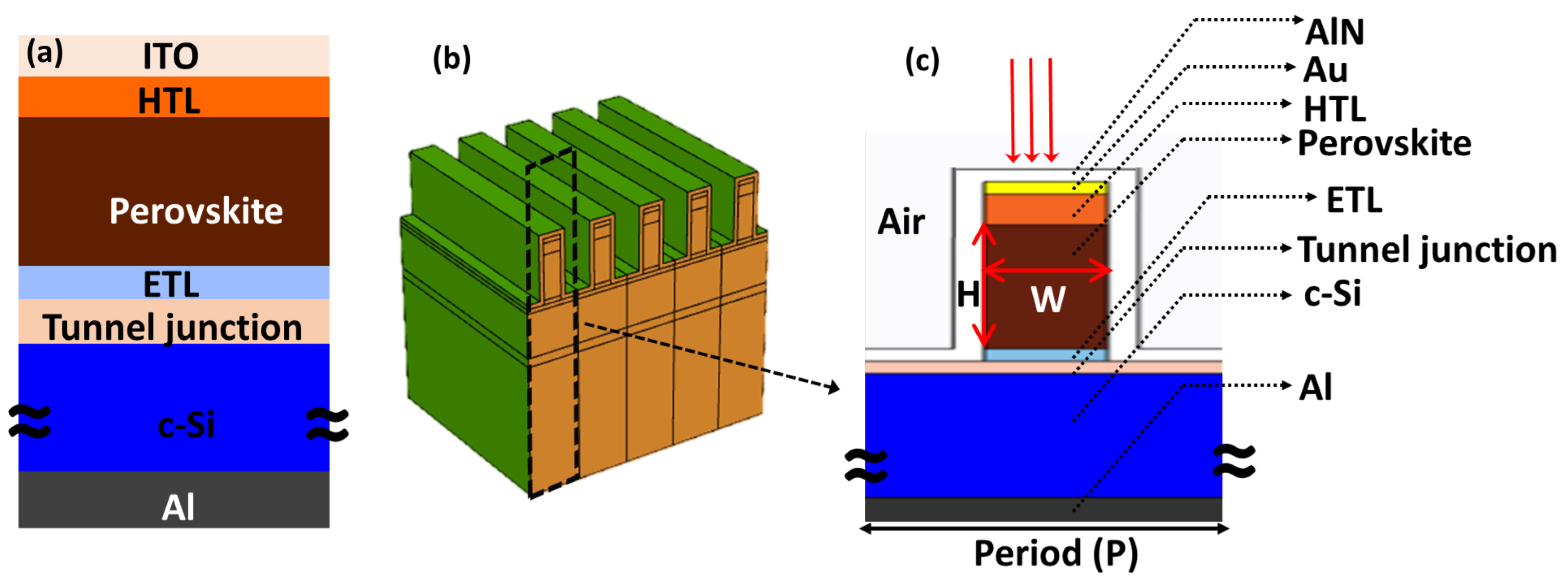
2. Design and Modeling

The layered structure for the planar perovskite/c-Si tandem solar cell shown in Figure 1a is one of the commonly used in other works [8,28,29]. Our nanostructured layer arrangement and design are shown in Figure 1b,c. The role, material and thickness of each layer are listed in Table 1, where they are ordered from top to bottom. When moving from the planar tandem cell to our design, we consider that the grating constitutes the upper cell. The materials of the core of the perovskite cell are the same for both designs. Table 1 also contains the references used to retrieve the optical constants of the materials.
The 5 nm-thick hydrogenated amorphous silicon layers are to facilitate the charge carrier transport in the c-Si subcell by generating the required built-in potential in the junction. Due to their small thickness, their optical effects are negligible and they will be ignored in our model [7,39]. In the proposed design we replaced the ITO thin film top contact with a nanostructured metallic electrode. The perovskite multilayer cell structure is distributed as a 1D rectangular grating on top of the cSi cell, which includes a gold thin film 20 nm-thick on top of it (refractive index from [32]). Figure 1b,c show the top perovskite cell layers arranged as a multilayer grating with a period P = 800 nm. As we see in Figure 1c, the width of the perovskite cell layers and the gold contact is the same, W. Both the width and the thickness of the perovskite layer, W and H, are the geometrical parameters that we optimized. Finally, we used a thin dielectric layer of aluminum nitride (AlN) as a protective coating. This material is being included in a wide variety of optoelectronic sensing devices because of its good biocompatibility and mechanic–electrical properties and is typically fabricated by sputtering technique [40]. The wavelength-dependent refractive index data for AlN was extracted from a standardized table [30]. Our design incorporates this material as a thin film, having a thickness of 50 nm. We have checked that the addition of this layer does not compromise the performance of the cell.
We calculated the optical performance of both the reference and proposed designs with the finite element method implemented in COMSOL Multiphysics. The nanostructured array is infinite along the grating direction and can be computationally reduced to a unit cell as shown in Figure 1b,c. Then, periodic boundary conditions applied on the sides of this unit cell to repeat it infinitely. The optical source is placed on top of the whole structure with a customized orientation that resembles the incidence conditions. The optical model evaluates absorption at each active layer, as well as the total reflection of the tandem cell. A detailed description of the optical model and the underlined equation are discussed and reported elsewhere [41]. The optical absorption in the perovskite and c-Si active layers is weighted with the spectral solar irradiance and is used to calculate the short-circuit current of each cell [7]. The structure is illuminated with transverse magnetic polarized light (TM) and transverse electric polarized light (TE) separately. Finally, we averaged both contributions to consider the unpolarized character of the solar irradiation.

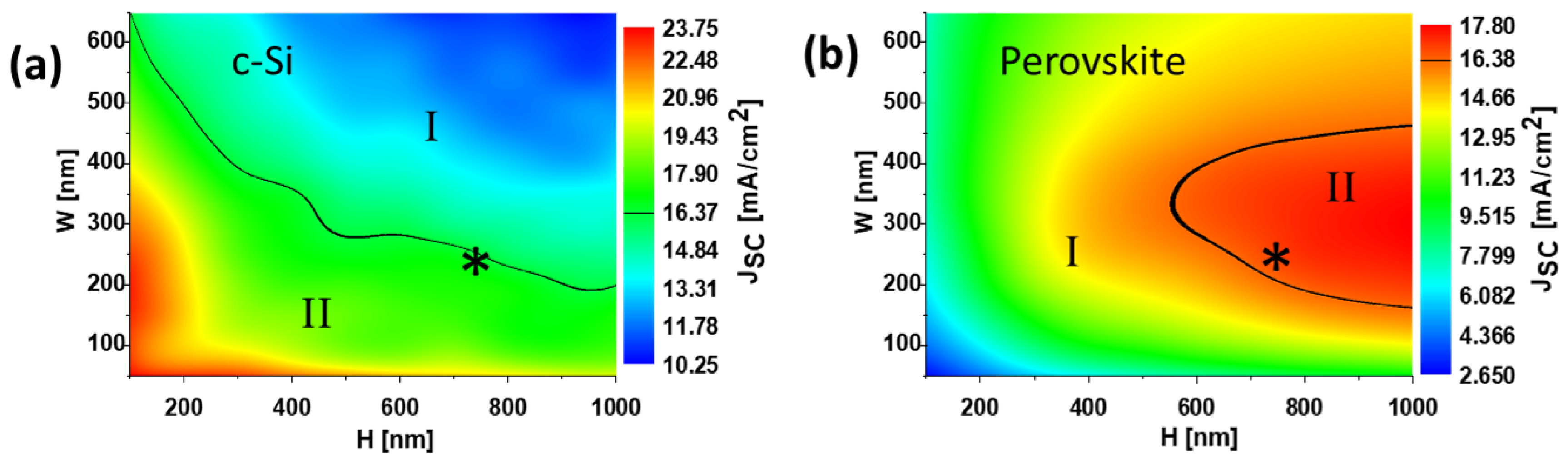
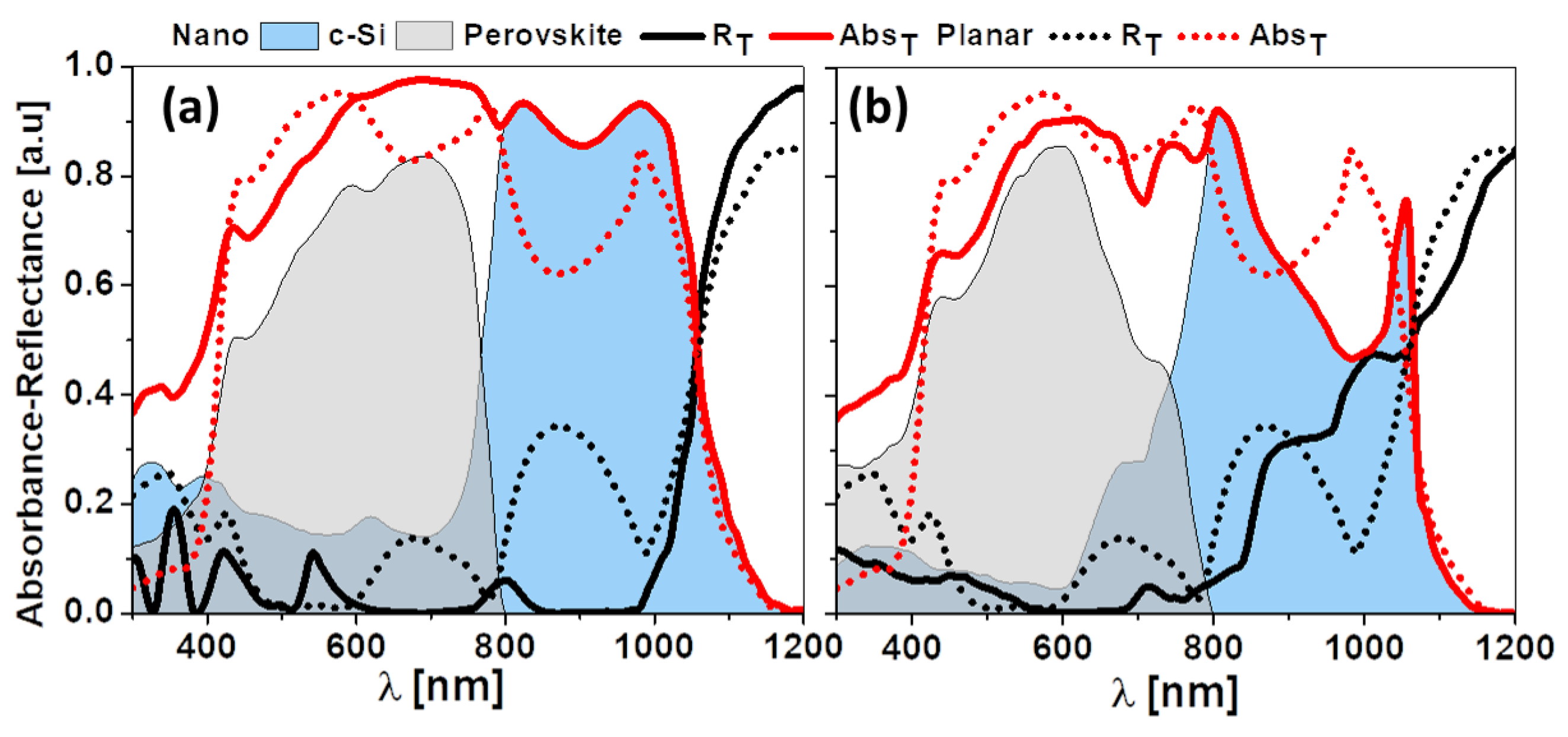
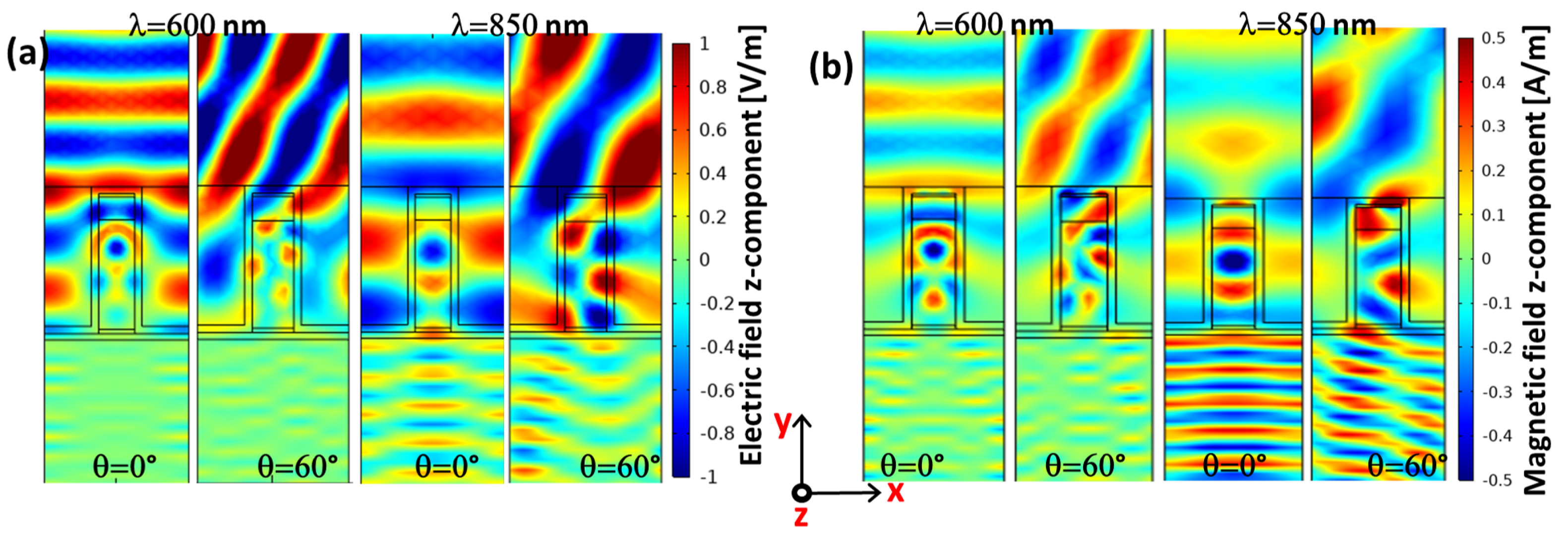
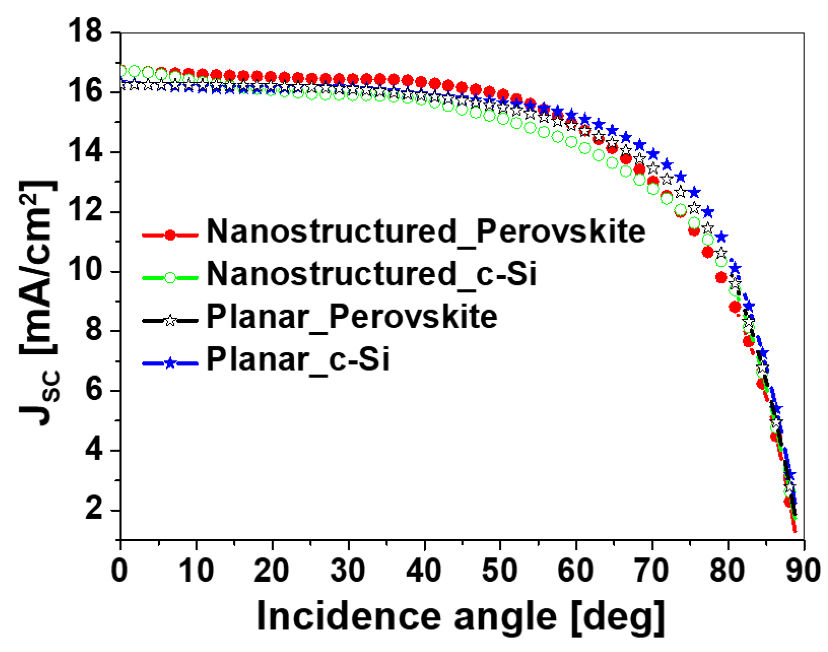
3. Results and Discussion

The duty cycle of the grating—the portion of the period occupied by the perovskite cell—determines the amount of short-wavelength irradiation that is absorbed by the perovskite cell and the energy transferred to the c-Si cell. It considers the radiation both directly through the gap of the grating, and after being transmitted through the perovskite cell. We optimized the design to maximize J S C from both junctions by considering the multilayered grating’s width, W, and the perovskite cell thickness, H. For a two-terminal tandem cell to operate properly, an additional condition must be fulfilled: currents from both device junctions need to be equal. This condition ensures that both junctions electrically matched, so that J S C (perovskite) = J S C (c-Si). Considering this electrical matching condition, the term J S C will refer to the short-circuit current of the individual cells.
We performed calculations with values of W between 50 nm and 650 nm (grating duty cycle ranging from 6.25% to 81.25%). The height ranges of the perovskite active layer went from 100 nm to 1000 nm. The diffusion length of the photo-generated charge carriers in perovskites is about 1 μm, so we limited the maximum height of the perovskite layer in our calculations to this value [42]. The results for the optimization calculation are shown in Figure 2. They show that increasing the width, W, generates a lower response from the c-Si cell (see Figure 2a). The same trend is observed when enlarging the thickness of the perovskite layer, H. The increase in both W and H leads to a larger volume of the perovskite multilayer and a higher absorption inside it, which leads to a lower generation of power at the c-Si cell. This result is expected because the perovskite multilayer extracts power from the incoming radiation, reducing the amount to be absorbed by the c-Si cell. The behavior of the perovskite cell is a little more complex (see Figure 2b). The delivered short-circuit current, J S C increases with thickness, H (more active medium involved), but it shows an optimum value for the width of the grating (≃50% duty cycle). The black lines in the maps of Figure 2a,b, define the geometrical parameters that yield the same J S C value as the reference planar device (16.2 mA/ cm 2 ) [7]. These lines divide the maps into two regions of interest: I and II. Region I corresponds to a J S C value lower than the value of J S C for the reference device with ITO and region II yields a J S C value higher than the one for the reference planar device. Therefore, the optimum geometry is in region II, where the design delivers a short-circuit current higher than the reference planar tandem cell. When choosing the geometrical arrangement of the grating lying in region II of both Figure 2a,b, we also need to fulfill the matching current condition. This situation is marked by the black star on the maps of Figure 2. It corresponds to a width W = 250 nm and a thickness H = 750 nm of the perovskite layer. The J S C value at this point is 16.7 mA/ cm 2 , which is 1.03 times the value of the reference planar device that uses an ITO top contact.
When analyzing the electromagnetic behavior of the proposed nanostructure, we observed how the top metallic contact efficiently redirects light towards the active layers of both devices. At the same time, the structure responds differently in terms of the polarization state of the incoming radiation. The results of this analysis is shown in Figure 3a,b for the TE and TM linear polarizations, respectively. Here, transversal means that the field vector is aligned along the grooves of the grating (perpendicular to the cross section presented in Figure 1c). The short wavelength portion is mostly absorbed by the active layer at the perovskite cell (shown in gray) and the long wavelength portion is absorbed by the active layer at the c-Si cell (shown in light blue). The sum of the absorption at both two active layers is plotted as a red solid line and the total reflection is plotted as a black solid line. The values of absorption at the active layers and total reflection for the reference planar ITO tandem cell are also represented as red and black dotted lines, respectively. Since the reference planar ITO tandem layer is polarization insensitive, the dotted lines are the same for both figures. These figures show that TE behaves better than TM for both parts of our nanostructured tandem cell. Moreover, the c-Si cell partially absorbs energy at short wavelengths as its surface is directly exposed to light. However, most of this absorption comes from the reduction in the total reflectance of the device. Our calculation of the short-circuit current uses the weighted absorption at the active layer with the AM1.5 solar spectrum. Based on these observations, we do not expect the final performance to degrade due to this absorption at short wavelengths at the c-Si cell. When averaging the TE and TM results, we obtained the performance for the unpolarized solar irradiation. Our design maximizes the short-circuit current of each cell. This optimization also provides a lower total reflectance for the proposed design (black solid line in Figure 3) when compared the reference planar device (black dashed line in Figure 3). This reduced total reflectance appears over the whole spectral range of the device.
Figure 4 shows the maps for the electric and magnetic field distributions for the TE and TM polarized light, respectively. We have evaluated these fields for two wavelengths, λ s = 600 nm and λ l = 850 nm, located at the spectral regions where the perovskite and c-Si cells absorb best, respectively. As expected, for λ s , the electric and magnetic fields are stronger at the perovskite cell, leaving almost no power for the c-Si cell to absorb. Additionally, for λ l , light is redirected by the grating towards the c-Si cell, generating larger field amplitudes. This trend is maintained for an angle of incidence of 60 .
In solar energy applications, solar cells receive sun irradiation from very different angles throughout the day. Therefore, solar cell devices must maintain a high performance under oblique illumination conditions. The dependence of the J S C value of perovskite and c-Si junctions with respect to the angle of incidence is shown in Figure 5. The values for the planar device is also included for comparison. Both devices behave almost the same through the whole angular range, with a slightly better performance of the nanostructured device at small angles of incidence (between 0 ° and 20 ° degree) and a little better performance of the planar device at large angles of incidence (from 40 ° to 60 ° degree). In any case, both devices maintain over 80% of their maximum performance value at normal incidence up 70 ° .

4. Conclusions

Transparent oxides are widely used to work as top contacts in solar cells. However, the advantage of these materials in terms of their electrical and optical properties is counterweighted by some other issues: their availability is limited, they are rigid and not easily applicable to flexible designs, and the fabrication technique may involve processes that can compromise the performance of the device. To replace these materials and maintain the functionality of the system, we have presented a novel arrangement for tandem solar cells that include perovskites on c-Si. The ITO top contact layer is removed, and a gold layer is placed on top of a periodic 1D multilayer grating. This periodic structure contains the perovskite cell of the tandem arrangement, where the c-Si cell is placed under the grating.
Our design optimizes the structure by maximizing the short-circuit current of the whole device when considering the solar spectral irradiance and its unpolarized character. To do this, we have used a computational electromagnetism package based on the finite element method that has been positively proved to describe the behavior of optoelectronic devices. The parameters used to optimize the system were: the width of the perovskite cell—which is directly related to the grating duty cycle—including the top metallic contact; and the thickness of the active layer of the perovskite cell. Using our simulations, we were able to balance the distribution of light between both cells and to generate an electrically matched tandem cell with a maximum short-circuit current. The calculated value of J SC is 1.03 times the value of the reference planar tandem cell that uses an ITO top contact. Reaching this value ensures that the replacement of the ITO top electrode does not degrade the efficiency of the cell. The computational evaluation considers unpolarized solar irradiation by averaging the results from TE and TM incidences. We also analyzed the dependence of the device’s performance with respect to the angle of incidence and we also observed a similar behavior of our device compared to the reference planar device with ITO contact.
In summary, the approach presented in this paper shows advantages over the typical design in terms of the availability and cost of the materials, while providing a comparable performance.

Author Contributions

All the authors, M.H.E., O.E., A.C. and J.A., contributed equally to this paper. All authors have read and agreed to the published version of the manuscript.

Funding

This work has been partially supported by the Spanish Ministry of Science, Innovation and Universities project NERA under grant RTI2018-101037-B-I00, and NANOROOMS under grant PID2019-105918GB-I00, by AEI/FEDER funds and by Comunidad de Madrid and FEDER Program SINFOTON2CM under grant S2018/NMT-4326, and TELURO under grant RTC2019-007113-3.

Institutional Review Board Statement

Not applicable.

Informed Consent Statement

Not applicable.

Acknowledgments

M.H. Elshorbagy thanks the Ministry of Higher Education of Egypt (missions section) for their supporting grant. Authors thank Irene Alda for her critical reading and English grammar and style revision of the manuscript.

Conflicts of Interest

The authors declare no conflict of interest.

References

  1. Shockley, W.; Queisser, H.J. Detailed balance limit of efficiency of p-n junction solar cells. J. Appl. Phys. 1961, 32, 510–519. [Google Scholar] [CrossRef]
  2. Zeitouny, J.; Katz, E.A.; Dollet, A.; Vossier, A. Band gap engineering of multi-junction solar cells: Effects of series resistances and solar concentration. Sci. Rep. 2017, 7, 1766. [Google Scholar] [CrossRef] [PubMed] [Green Version]
  3. Zhu, S.; Yao, X.; Ren, Q.; Zheng, C.; Li, S.; Tong, Y.; Shi, B.; Guo, S.; Fan, L.; Ren, H.; et al. Transparent electrode for monolithic perovskite/silicon-heterojunction two-terminal tandem solar cells. Nano Energy 2018, 45, 280–286. [Google Scholar] [CrossRef]
  4. Park, I.J.; Park, J.H.; Ji, S.G.; Park, M.A.; Jang, J.H.; Kim, J.Y. A three-terminal monolithic perovskite/Si tandem solar cell characterization platform. Joule 2019, 3, 807–818. [Google Scholar] [CrossRef] [Green Version]
  5. Kanoun, A.A.; Goumri-Said, S.; Kanoun, M.B. Device design for high-efficiency monolithic two-terminal, four-terminal mechanically stacked, and four-terminal optically coupled perovskite-silicon tandem solar cells. Int. J. Energy Res. 2021, 45, 10538–10545. [Google Scholar] [CrossRef]
  6. Werner, J.; Barraud, L.; Walter, A.; Brauninger, M.; Sahli, F.; Sacchetto, D.; Tetreault, N.; Paviet-Salomon, B.; Moon, S.J.; Allebe, C.; et al. Efficient Near-Infrared-Transparent Perovskite Solar Cells Enabling Direct Comparison of 4-Terminal and Monolithic Perovskite/Silicon Tandem Cells. ACS Energy Lett. 2016, 1, 474–480. [Google Scholar] [CrossRef]
  7. Elshorbagy, M.H.; López-Fraguas, E.; Chaudhry, F.A.; Sánchez-Pena, J.M.; Vergaz, R.; García-Cámara, B. A monolithic nanostructured-perovskite/silicon tandem solar cell: Feasibility of light management through geometry and materials selection. Sci. Rep. 2020, 10, 2271. [Google Scholar] [CrossRef] [Green Version]
  8. Jost, M.; Kegelmann, L.; Korte, L.; Albrecht, S. Monolithic perovskite tandem solar cells: A review of the present status and advanced characterization methods toward 30% efficiency. Adv. Energy Mater. 2020, 10, 1904102. [Google Scholar] [CrossRef]
  9. Kim, J.Y.; Lee, J.W.; Jung, H.S.; Shin, H.; Park, N.G. High-efficiency perovskite solar cells. Chem. Rev. 2020, 120, 7867–7918. [Google Scholar] [CrossRef]
  10. Lal, N.N.; Dkhissi, Y.; Li, W.; Hou, Q.; Cheng, Y.B.; Bach, U. Perovskite tandem solar cells. Adv. Energy Mater. 2017, 7, 1602761. [Google Scholar] [CrossRef]
  11. Afre, R.A.; Sharma, N.; Sharon, M.; Sharon, M. Transparent conducting oxide films for various applications: A review. Rev. Adv. Mater. Sci. 2018, 53, 79–89. [Google Scholar] [CrossRef]
  12. Ho, S.M. A review on thin films on indium tin oxide coated glass substrate. Asian J. Chem. 2016, 28, 469–472. [Google Scholar] [CrossRef]
  13. Liu, H.; Avrutin, V.; Izyumskaya, N.; Ozgur, U.; Morkoc, H. Transparent conducting oxides for electrode applications in light emitting and absorbing devices. Superlattices Microstruct. 2010, 48, 458–484. [Google Scholar] [CrossRef]
  14. Blake, J.; Paynton, R. Transparent Film and Substrate Technology for Touch Screens and Flexible-Display Applications. Inf. Disp. 2011, 27, 34–38. [Google Scholar] [CrossRef]
  15. Haldar, A.; Yambem, S.D.; Liao, K.S.; Alley, N.J.; Dillon, E.P.; Barron, A.R.; Curran, S.A. Organic photovoltaics using thin gold film as an alternative anode to indium tin oxide. Thin Solid Films 2011, 519, 6169–6173. [Google Scholar] [CrossRef]
  16. Alfantazi, A.M.; Moskalyk, R. Processing of indium: A review. Miner. Eng. 2003, 16, 687–694. [Google Scholar] [CrossRef]
  17. Ramadan, R.; Abdel-Hady, K.; Manso-Silván, M.; Torres-Costa, V.; Martín-Palma, R.J. Microwave plasma and rapid thermal processing of indium-tin oxide thin films for enhancing their performance as transparent electrodes. J. Photonics Energy 2019, 9, 034001. [Google Scholar] [CrossRef]
  18. Lim, J.W.; Cho, D.Y.; Na, S.I.; Kim, H.K. Simple brush-painting of flexible and transparent Ag nanowire network electrodes as an alternative ITO anode for cost-efficient flexible organic solar cells. Sol. Energy Mater. Sol. Cells 2012, 107, 348–354. [Google Scholar] [CrossRef]
  19. Zhang, J.; Hu, X.; Li, H.; Ji, K.; Li, B.; Liu, X.; Xiang, Y.; Hou, P.; Liu, C.; Wu, Z.; et al. High-Performance ITO-Free Perovskite Solar Cells Enabled by Single-Walled Carbon Nanotube Films. Adv. Funct. Mater. 2021, 31, 2104396. [Google Scholar] [CrossRef]
  20. Spinelli, P.; Fuentes Pineda, R.; Scigaj, M.; Ahmad, T.; Wojciechowski, K. Transparent conductive electrodes based on co-sputtered ultra-thin metal layers for semi-transparent perovskites solar cells. Appl. Phys. Lett. 2021, 118, 241110. [Google Scholar] [CrossRef]
  21. Aleem, M.; Vishnuraj, R.; Krishnan, B.; Pullithadathil, B. Realization of Micropatterned, Narrow Line-Width Ni–Cu–Sn Front Contact Grid Pattern Using Maskless Direct-Write Lithography for Industrial Silicon Solar Cells. ACS Appl. Energy Mater. 2021, 4, 10682–10696. [Google Scholar] [CrossRef]
  22. Tang, G.; Yan, F. Recent progress of flexible perovskite solar cells. Nano Today 2021, 39, 101155. [Google Scholar] [CrossRef]
  23. Zhu, J.; Zhu, X.; Hoekstra, R.; Li, L.; Xiu, F.; Xue, M.; Zeng, B.; Wang, K.L. Metallic nanomesh electrodes with controllable optical properties for organic solar cells. Appl. Phys. Lett. 2012, 100, 143109. [Google Scholar] [CrossRef] [Green Version]
  24. Stelling, C.; Singh, C.R.; Karg, M.; König, T.A.; Thelakkat, M.; Retsch, M. Plasmonic nanomeshes: Their ambivalent role as transparent electrodes in organic solar cells. Sci. Rep. 2017, 7, 42530. [Google Scholar] [CrossRef]
  25. Li, J.; Wang, H.; Chin, X.Y.; Dewi, H.A.; Vergeer, K.; Goh, T.W.; Lim, J.W.M.; Lew, J.H.; Loh, K.P.; Soci, C.; et al. Highly efficient thermally co-evaporated perovskite solar cells and mini-modules. Joule 2020, 4, 1035–1053. [Google Scholar] [CrossRef]
  26. Zhang, Z.; Ji, R.; Kroll, M.; Hofstetter, Y.J.; Jia, X.; Becker-Koch, D.; Paulus, F.; Löffler, M.; Nehm, F.; Leo, K.; et al. Efficient Thermally Evaporated γ-CsPbI3 Perovskite Solar Cells. Adv. Energy Mater. 2021, 11, 2100299. [Google Scholar] [CrossRef]
  27. Feleki, B.T.; Weijtens, C.H.; Wienk, M.M.; Janssen, R.A. Thin Thermally Evaporated Organic Hole Transport Layers for Reduced Optical Losses in Substrate-Configuration Perovskite Solar Cells. ACS Appl. Energy Mater. 2021, 4, 3033–3043. [Google Scholar] [CrossRef]
  28. Hou, F.; Yan, L.; Shi, B.; Chen, J.; Zhu, S.; Ren, Q.; An, S.; Zhou, Z.; Ren, H.; Wei, C.; et al. Monolithic perovskite/silicon-heterojunction tandem solar cells with open-circuit voltage of over 1.8 V. ACS Appl. Energy Mater. 2019, 2, 243–249. [Google Scholar] [CrossRef]
  29. Köhnen, E.; Jošt, M.; Morales-Vilches, A.B.; Tockhorn, P.; Al-Ashouri, A.; Macco, B.; Kegelmann, L.; Korte, L.; Rech, B.; Schlatmann, R.; et al. Highly efficient monolithic perovskite silicon tandem solar cells: Analyzing the influence of current mismatch on device performance. Sustain. Energy Fuels 2019, 3, 1995–2005. [Google Scholar] [CrossRef] [Green Version]
  30. Pastrnak, J.; Roskovcova, L. Refraction index measurements on AlN single crystals. Phys. Status Solidi (B) 1966, 14, K5–K8. [Google Scholar] [CrossRef]
  31. Konig, T.A.; Ledin, P.A.; Kerszulis, J.; Mahmoud, M.A.; El-Sayed, M.A.; Reynolds, J.R.; Tsukruk, V.V. Electrically tunable plasmonic behavior of nanocube–polymer nanomaterials induced by a redox-active electrochromic polymer. ACS Nano 2014, 8, 6182–6192. [Google Scholar] [CrossRef] [PubMed]
  32. Johnson, P.B.; Christy, R.W. Optical constants of the noble metals. Phys. Rev. B 1972, 6, 4370. [Google Scholar] [CrossRef]
  33. Filipic, M.; Loper, P.; Niesen, B.; De Wolf, S.; Krc, J.; Ballif, C.; Topic, M. CH 3 NH 3 PbI 3 perovskite/silicon tandem solar cells: Characterization based optical simulations. Opt. Express 2015, 23, A263–A278. [Google Scholar] [PubMed] [Green Version]
  34. Loper, P.; Stuckelberger, M.; Niesen, B.; Werner, J.; Filipic, M.; Moon, S.J.; Yum, J.H.; Topic, M.; De Wolf, S.; Ballif, C. Complex refractive index spectra of CH3NH3PbI3 perovskite thin films determined by spectroscopic ellipsometry and spectrophotometry. J. Phys. Chem. Lett. 2015, 6, 66–71. [Google Scholar] [CrossRef]
  35. Siefke, T.; Kroker, S.; Pfeiffer, K.; Puffky, O.; Dietrich, K.; Franta, D.; Ohlídal, I.; Szeghalmi, A.; Kley, E.B.; Tünnermann, A. Materials pushing the application limits of wire grid polarizers further into the deep ultraviolet spectral range. Adv. Opt. Mater. 2016, 4, 1780–1786. [Google Scholar] [CrossRef]
  36. Vora, A.; Gwamuri, J.; Pearce, J.M.; Bergstrom, P.L.; Güney, D.Ö. Multi-resonant silver nano-disk patterned thin film hydrogenated amorphous silicon solar cells for Staebler-Wronski effect compensation. J. Appl. Phys. 2014, 116, 093103. [Google Scholar] [CrossRef] [Green Version]
  37. Nguyen, H.T.; Rougieux, F.E.; Mitchell, B.; Macdonald, D. Temperature dependence of the band-band absorption coefficient in crystalline silicon from photoluminescence. J. Appl. Phys. 2014, 115, 043710. [Google Scholar] [CrossRef]
  38. McPeak, K.M.; Jayanti, S.V.; Kress, S.J.; Meyer, S.; Iotti, S.; Rossinelli, A.; Norris, D.J. Plasmonic films can easily be better: Rules and recipes. ACS Photonics 2015, 2, 326–333. [Google Scholar] [CrossRef]
  39. Elshorbagy, M.H.; García-Cámara, B.; López-Fraguas, E.; Vergaz, R. Efficient light management in a monolithic tandem perovskite/silicon solar cell by using a hybrid metasurface. Nanomaterials 2019, 9, 791. [Google Scholar] [CrossRef] [Green Version]
  40. Mariello, M.; Guido, F.; Algieri, L.; Mastronardi, V.M.; Qualtieri, A.; Pisanello, F.; De Vittorio, M. Microstructure and Electrical Properties of Novel piezo-optrodes Based on Thin-Film Piezoelectric Aluminium Nitride for Sensing. IEEE Trans. Nanotechnol. 2020, 20, 10–19. [Google Scholar] [CrossRef]
  41. Elshorbagy, M.H.; Alda, J. Funneling and guiding effects in ultrathin aSi-H solar cells using one-dimensional dielectric subwavelength gratings. J. Photonics Energy 2017, 7, 017002. [Google Scholar] [CrossRef] [Green Version]
  42. Loi, M.A.; Hummelen, J.C. Perovskites under the Sun. Nat. Mater. 2013, 12, 1087–1089. [Google Scholar] [PubMed]
Figure 1. (a) Layered structure of the reference planar tandem perovskite/c-Si solar cell (the active c-Si is much thicker than the rest of the layer). (b) Schematic design of a nanostructured perovskite solar cell located on top of a crystalline silicon cell. (c) Detailed cross section of the layer structure. This corresponds with the unit cell in the simulations.
Applsci 12 01854 g001
Figure 2. Short-circuit current maps in terms of the thickness, H, and width, W of the perovskite layer, for the c-Si cell (a) and the perovskite cell (b). The black line represents the value of the short-circuit current obtained for the reference planar cell. Regions I and II contain the configuration delivering a smaller or larger J S C than the planar tandem cell, respectively. The black star denotes the configuration selected in this contribution, meeting the equal short-circuit current condition in both cells of the tandem configuration.
Applsci 12 01854 g002
Figure 3. Absorption and reflection for (a) TE and (b) TM cases. The gray color region represents the absorption of the perovskite active layer and the light blue color region is for the absorption at the c-Si active layer. The red solid line denotes the total absorption in the active layer for both of them and the black solid line is the total reflection of the nanostructure cell. The red and black dotted lines show the total absorption in perovskite and c-Si active layers and total reflection for the planar solar cell, respectively.
Applsci 12 01854 g003
Figure 4. Electric field (a) and magnetic field (b) maps for the TE and TM polarizations, respectively. These maps were calculated for short and long wavelengths ( λ s = 600 nm and λ l = 850 nm), and for normal and oblique incidence conditions ( θ = 0 and θ = 60 ).
Applsci 12 01854 g004
Figure 5. Short-circuit current as a function of the angle of incidence for the nanostructured and planar solar cells. The red line with closed circles is for the perovskite cell and the green line with open circles is for the c-Si in the nanostructure cell. The black line with open stars is for the perorvskite cell and the blue line with closed stars is for the c-Si in the planar cell.
Applsci 12 01854 g005
Table 1. Tandem perovskite/c-Si solar cell layer structure. Both the materials and thicknesses of the layers are included for the planar cell and the one presented in this paper (nanostructured). We have also included the references where the optical constant are taken from.
LayerMaterial
(Planar Cell → Nanostructured)
Thickness
(Planar Cell → Nanostructured)
ProtectiveNone → AlN [30]0 → 50 nm
Top contactITO [31] → Au grating [32]100 nm → 20 nm
Hole transport layer (HTL)SPIRO-OMeTAD [33]160 nm
Active layerPerovskite ( CH 3 NH 3 PbI 3 ) [34]260 nm → 750 nm
Electron transport layer (ETL) TiO 2 [35]30 nm
Tunnel junctionITO [31]44 nm
Hole transportp-type hydrogenated amorphous silicon (paSi-H) [36]10 nm
Buffer layerintrinsic hydrogenated amorphous silicon (iaSi-H) [36]5 nm
Active layerCrystalline Si (c-Si) [37]200 μ m
Buffer layerIntrinsic hydrogenated amorphous silicon (iaSi-H) [36]5 nm
Electron transport layern-type hydrogenated amorphous silicon(naSi-H) [36]10 nm
Botton contactAluminum (Al) [38]200 nm
Publisher’s Note: MDPI stays neutral with regard to jurisdictional claims in published maps and institutional affiliations.

