Abstract
Photonic transmitters that operate with a high data transfer rate (over 150 Gb/s) at the O-band range (1260–1360 nm) require at least 100 milliwatts of power to overcome the power losses that are caused by using high-speed modulators. A laser with higher power can probably handle this requirement; however, for the transmitter system, this solution can be problematic due to the nonlinear effects that can happen, which may lead to high noise in the transmitter system. Thus, to solve this issue, we propose a new design of a 2 × 1 multimode interference (MMI) power combiner using silicon nitride (SiN) slot waveguide structures. The MMI power combiner and the SiN slot waveguide structures were optimized using the full-vectorial beam propagation method (FV-BPM) and the finite difference time domain (FDTD) method. After combining two sources, high efficiency was obtained of 94.8–97.6% from the total power after a short coupling length of 109.81 µm over the O-band range with a low back reflection of 44.94 dB. Thus, the proposed device can be very useful for combining two O-band sources to gain a higher power level, which can be utilized to improve performances in transmitter systems.
1. Introduction
Photonic integrated circuits are attracting great interest, fueled by several recent developments, such as the booming sector of mixed reality (MR), which includes virtual reality (VR) and augmented reality (AR) [1]. Massive efforts are being put into the VR sector due to extensive use by military forces around the globe [2]. A VR head-up device is a classic glasses-like device that allows the user to experience a completely virtual reality environment generated by complex optical systems, such as high-end displays, cameras, and iris sensors [2]. These optical systems must keep up with the user requirements, where the body movements (hands, legs, eyes, head, etc.) are tracked, analyzed, and the data are plotted accordingly. Thus, faster body movement speed demands more optical abilities in these photonic systems. Optical power combiners are a main pillar optical element in VR headsets, as they are the base of the connection between the digital world, the real world, and the user’s eyes [3].
This high demand for transmitting data in several applications has led to the use of high-bitrate modulator devices which can function well under this rate but with more power losses [4]. To overcome these losses, a higher laser source power is needed with 100 milliwatts at least, or using a complex modulator structure [5]. A high-power laser may be used to solve this issue; however, this type of laser may limit the transmitter system’s performance due to the nonlinear effects [6,7]. Thus, a better option for obtaining a higher power level from a standard laser is to use a waveguide coupler that can combine several standard laser sources without nonlinear effects.
A slot waveguide is a superior waveguide [8] that can guide and confine light with a very low power loss due to a unique property, which is strong light confinement inside the slot area in case of transverse magnetic or slab areas in case of transverse electric (TE) mode [9]. This structure is based on three layers, two high index layers (slabs) and a low index layer (slot), which ensures total internal reflection (TIR) and is an important light confinement mechanism of the slot waveguide [10].
One more important phenomenon of the slot waveguide operation is the discontinuity of the electric field at the boundaries between the different materials. The discontinuity is present in the perpendicular electric field component of the electromagnetic wave in TE mode at the slot boundaries. This analysis, which is based on Maxwell’s equations, shows that the electric field is much more intense in the low refractive index slot region than in the high refractive index regions, resulting in a relatively higher power density in the slot than that in the high refractive index regions [8].
Slot waveguide structure is widely used in sensitive biochemical optical integrated sensors, such as ring resonator-based refractometric label-based optical sensing, and nano-opto-mechanical sensors. The conventional strip or rib waveguides are often used in biochemical sensors based on integrated photonics. In these waveguides, the light is guided based on total TIR in a high refractive index material, surrounded by a low refractive index material; the TIR confines light in the high refractive index material. However, the mentioned waveguides are more wavelength-dependent than slot waveguides because of the relatively high optical interference [11]. These great abilities make the slot waveguide a good candidate for designing new waveguide devices such as splitters [12], demultiplexers [13,14], combiners [15], and optical amplification [16].
Multimode interference (MMI) based photonic devices is a key building block for designing photonic integrated circuits because of their unique structure, low polarization dependence, large bandwidth, and low excess loss [17,18]. The operation principle of MMI devices is based on the self-imaging mechanism, which is the ability to reproduce the input field pattern in single or multiple images at periodic intervals over the propagation axis of the device over the waveguide [19]. MMI devices are used for many applications such as filters [20], temperature sensors [21], splitters [22,23], and couplers [24].
Several combiners have been introduced in recent works such as diffractive, anisotropic photonic crystal-based (photonic bandgap) combiners, and holographic combiners; holographic combiners are thin optical combiners that use diffraction to transform an incident wavefront into another. They can be used as lenses or as non-flat mirrors and have several applications in photonic optical systems [25].
Another widely spread photonic combiner is the photonic crystal-based (photonic bandgap) combiner. Its structure and operating mechanism, as presented in [26], are determined by specific features such as photonic bands, photonic bandgap, resonant interaction of photons with the periodic lattice, and constructive and destructive interferences [26]; however, one of the best known drawbacks of photonic crystal devices is the extreme cost of fabrication.
Among the recent and many other combiners, waveguide combiners are based on total internal reflection (TIR) propagation of the entire field in an optical waveguide, essentially acting as a transparent periscope with a single entrance taper and often many exit tapers. When the number of TIR bounces increases, one might refer to them as waveguide combiners. The main components of a waveguide combiner consist of the input and output couplers. These can be either simple prisms, microprism arrays, embedded mirror arrays, surface relief gratings (SRGs), thin or thick analog holographic gratings, meta-surfaces, or resonant waveguide gratings (RWGs) [3]. All of these have their specific advantages and limitations, which will be discussed here. Waveguide combiners have been used historically over a vast range of applications, ranging from AR combiners, such as planar optical interconnections, to LCD backlights [27].
The photonic power combiner is a key component in transmitter systems that require a high-power level. There are usually two types of photonic power combiners, which are power combiners and multiplexers also called wavelength combiners. MMI couplers can be designed as a power combiner for combining many optical signals with the same wavelength or different wavelengths. However, the power loss is relatively high in such components. For example, researchers demonstrated a 4 × 1 MMI coupler that has a very low power of 6 dB for each operated wavelength [18]. Some examples of multiplexer or wavelength couplers based on waveguide technologies are ring-resonator filters [28], and photonic bandgap filters [29] have been demonstrated. Wavelength combiners typically have a short band, which can cause distortion between the operating wavelengths. In addition, wavelength combiners in a practical system can reach a lower power level because of the fabrication process errors, which can happen as a result of small deviations in the dimensions of the device [30].
With the amount of information generated by 5G applications, cloud computing is always fueling the need for increasing data bitrates and better energy-efficient photonic interconnections in data center systems [31]. Silicon photonic transmitters depend on high-speed modulator devices, such as micro-ring, Mach-Zehnder, and electro-absorption devices, which are used to satisfy evolving bandwidth and energy requirements as they can combine energy efficiency, compact footprint, and complementary metal-oxide semiconductor compatibility [32,33].
The back reflection is the amount of light reflected from the output waveguide; such a phenomenon can occur due to the differences in the reflective indexes between the waveguide materials along the boundaries. Therefore, one of the main problems that can limit the performance of the transmitter system is the back reflection coming back to the laser source [13]. The silicon MMI coupler can gain reflections from the self-imaging mechanism, because of its high index difference between silicon and silica (SiO2) [13]. However, a low index material such as silicon nitride (SiN) can be a great solution because of its good properties [34,35,36] such as a low refractive index, low absorption at the O-band range, and low thermal sensitivity.
The index contrast between silicon and SiO2 or SiN and SiO2 has a great influence on the waveguide guiding properties [37]. The index contrast in silica cladded silicon is around 145% and this index contrast does not change significantly with the signal shift. In a silica cladded SiN platform, the index contrast is around 35% at the O-band range. The benefits provided by the higher index contrast of the silicon platform as compared to the SiN platform come with the tradeoff of enhanced sensitivity of silicon devices to nanometer-scale geometrical variations. These can come from the thickness variation of the silicon layer or errors in the fabrication process, which means variations in width and etch depth of the waveguides. All these results can cause effective index deviations from the desired parameter value, which is a critical key parameter for the MMI coupler device. Therefore, it is better to use a SiN platform for the MMI coupler that functions at the O-band window.
In this study, we propose a new design of a 2 × 1 MMI power combiner based on SiN slot waveguide structures that operate on the O-band spectrum under a TE polarization mode. Optimizations of the key structure geometrical parameters were done using the full-vectorial beam propagation method (FV-BPM) and the finite difference time domain (FDTD) method for obtaining high power confinement, self-imaging, and higher-level power. Input tapers and the output taper were integrated into the MMI coupler for reducing the back reflection losses. This study shows how to design a combiner which can combine two coherent laser sources operating in the O-band range, which can achieve better performance results for the transmitter systems.
2. The 2 × 1 MMI Power Combiner Design and Theoretical Aspects
Figure 1a shows the refractive index profile of the slot waveguide for the two input tapers at z = 0 µm for a 1310 nm operating wavelength. In this figure, the red color areas are SiN with an index of 1.994 over a thickness of 348 nm, pink areas are SiO2 with an index of 1.444 over the cover and the slot regions. The slot thickness is 98 nm and as can be seen, it is located between the two slab layers (red color) shown in Figure 1a. Figure 1b shows a sketch of the MMI coupler for combining two laser sources and the taper input waveguides and the output at the x-z plane. In this figure, WMMI is the width of the MMI coupler, LMMI is the length of the MMI coupler and gap is the distance between the two input tapers.
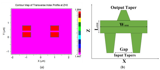
Figure 1.
2 × 1 power combiner structure design: (a) slot waveguide refractive index profile at the x-y plane; (b) full schematic sketch of the MMI coupler with the taper waveguides at the x-z plane.
The beat length of the MMI combiner coupler is given by [15]:
The beat length is a key parameter that sets the MMI coupler length as shown in Equation (3). In this equation, λ is the wavelength, neff is the mode effective index, and We is the effective width of the MMI coupler, which depends on the polarization mode as can be seen in Equation (2), which is given by [15]:
where σ = 0 in case of TE mode and σ = 1 for TM mode polarization. Thus, for obtaining a more compact device it is better to select TE mode polarization. The MMI coupler length is given by [15]:
where p is a positive number and N is the number of laser sources. In our study, N = 2 (two laser sources) and p = 1, which were selected for obtaining a shorter MMI coupler length. The insertion loss of the combiner device is described by the next expression:
where Pout is the output power of the combiner and Pin is the input laser power.
The adiabatic condition rule for designing the inputs and output waveguide taper is given by [38,39]:
where θ is the half-angle of the taper at the z-axis, and W is the local full width of the taper. The rule requires that the spreading of the waveguide sidewalls needs to be slower than the diffraction spreading of the fundamental mode, and this can happen by selecting an optimal waveguide taper length that satisfies this rule. Thus, the fundamental mode is well confined inside the tapered waveguide and no mode conversion to other higher-order modes can happen.
3. Simulation Results
The numerical investigations of the 2 × 1 MMI power combiner based on using SiN slot-waveguide structures were performed using Rsoft-cad software. The data from FV-BPM and FDTD results were analyzed using MATLAB codes. Figure 2a shows the solution of the TE fundamental polarization mode and the mode profile at the x-y plane for two Gaussian laser sources that work at 1310 nm wavelength.
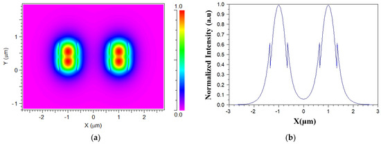
Figure 2.
Solution of the TE fundamental mode for 2 × 1 power combiner: (a) Ey polarization mode profile; (b) horizontal view at y = 220 nm.
As can be seen in the red color areas, a high intensity is obtained inside the SiN layers as expected from the light behavior under TE mode in the slot waveguide. Thus, a large range of high intensity is obtained over the y-axis with 794 nm. This large range can be useful for improving the light coupling adjustment between the two laser sources and the input waveguide taper over the y-axis. It is important to clarify that Figure 2a shows the profile of the TE fundamental polarization mode and not the physical location of the lasers. This means that the gap between the laser can be seen, as in Figure 1a.
The gap between the two laser sources was set to 1.4 μm, for the sake of diminishing the possibility of light coupling, as shown in Figure 2a. Usually, in classical waveguide techniques, the spacing is set to be over 2 μm but, in our case, the slot waveguide allowed us to gain powerful light confinement, so it could be utilized to choose a narrower gap. According to the solutions of the TE fundamental polarization mode, we also optimized the grid convergence size in the x-axis and the y-axis to 20 nm and the z-axis to 15 nm using FV-BPM. These sizes were utilized for all other FV-BPM simulations.
The normalized intensity level for the two sources over the x-axis at y = 250 nm, which is located at the SiN layer, as can be seen in Figure 2b.
The neff value was extracted by solving the fundamental mode inside the SiN slot waveguide and its value was 1.715. To obtain a compact combiner device the width of the MMI combiner coupler was set to 3.55 μm. We and Lπ were calculated using Equations (1) and (2) for the TE mode operation and their results were 2.94 μm and 15.13 μm, respectively. The optimal size of the MMI coupler length was found using FV-BPM simulations combined with MATLAB codes and the value was 9.81 μm.
Figure 3a,b shows the optimizations of the MMI combiner coupler and the tolerance range for the length and the width of the MMI combiner coupler. The width of the MMI coupler tolerance range was 3.48 to 3.62 μm; this value was suitable to transmit more than 97% of the total power, as shown in Figure 3a. The length of the MMI coupler tolerance range was 9.6 to 10.1 μm, which was also ideal to transmit more than 97% of the total power, as shown in Figure 3b. From the fabrication overview, these tolerance parameter values were more than 200 nm for LMMI and 70 nm for WMMI from the optimal values. Thus, these results are considered great for a facility with a high accuracy of ±40 nm from the optimal geometrical parameter. These tolerance ranges could also be utilized for the test structure measurements, which usually help to find the parameter’s geometrical errors by comparing the experimental results to the theoretical results, as shown in Figure 3a,b.
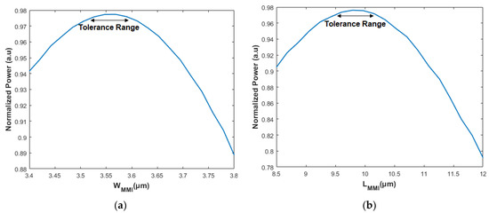
Figure 3.
Normalized power as a function of the MMI combiner coupler key parameters: (a) WMMI (b) LMMI.
The input/output waveguide taper length was optimized to be suitable to the width changing size from 0.6 to 1.318 μm, while keeping the mode solution stable, also called the adiabatic condition of the taper. From Figure 4, it can be seen that at more than 10 μm, a normalized power level of 97% was obtained, however this length did not match the adiabatic condition, which is described in Equation (5). Thus, by solving the taper mode, the suitable length was found and its value was 50 μm with a normalized power of more than 97.5% of the total power.
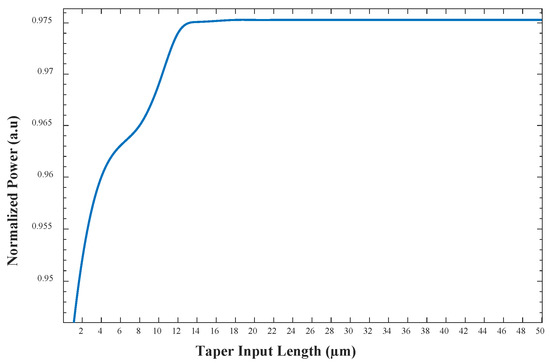
Figure 4.
Optimizations of the waveguide taper length.
Figure 5a shows the light intensity profile of two Gaussian TE fields at the signal of 1.31 μm at the x-z plane. The Gaussian source was set to be 50% of the total laser power level. It can be noted that the light intensity was combined from two sources to one source at z = 59.81 μm. The selected gap between the two input laser sources ensured there was no light coupling between them, as can be seen in Figure 5a in the input taper section. After a short light coupling of 109.81 µm, the combiner efficiency reached 97.6% from the total input power coming from the two sources, as shown in Figure 5b. Thus, the insertion loss could be calculated using Equation (4) at 1310 nm wavelength and the power loss value was only 0.105 dB.
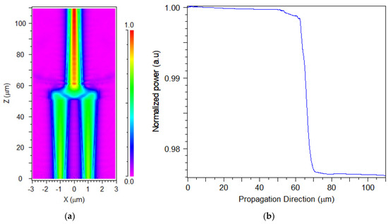
Figure 5.
2 × 1 combiner intensity light propagation profile under TE mode: (a) plane x-z; (b) z-axis.
Figure 6 shows the normalized power as a function of the wavelength over the O-band spectrum, and it can be seen that a high combiner efficiency range of 94.8–97.6% from the total power was obtained. The wavelength tolerance range over the O-band was 1280 to 1330 nm, which is suitable to transmit more than 96.3% of the total power, as shown in Figure 6. Thus, the proposed combiner could easily handle the laser wavelength drift effect, and heat emissions during the natural working process of a laser. Therefore, this coupler could be suitable for combining lasers and worrying less about the wavelength drift effect over the O-band range.
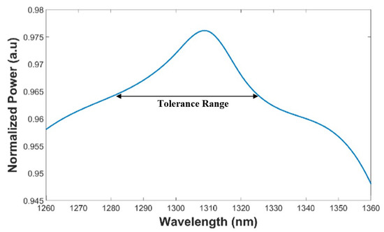
Figure 6.
Normalized optical power of the MMI combiner versus wavelength over the O-band spectrum.
The back reflection coming back from the MMI coupler into the laser source is an undesirable phenomenon because of its potential to amplify noises in the laser system. The back reflection can happen because of the self-imaging mechanism and the high index differences between the index waveguide material and the cover index material. However, in our design, the back reflection was not an issue thanks to SiN slot waveguide technology combined with waveguide tapers, which can easily deal with the reflections coming from the MMI coupler and the SiO2 cover area. To demonstrate the advance of using this technology, a FDTD simulation was done to calculate the power back reflection of the proposed combiner at the wavelength of 1310 nm. Figure 7a shows the schematic sketch of the FDTD simulation setup, which includes the full 2 × 1 combiner design with an additional SiN waveguide segment that is used for setting the monitor. This monitor collects the light reflections coming back into the input waveguide tapers, as shown in Figure 7a. The grid size for all dimensions (x-axis, y-axis, z-axis) was set to 10 nm for obtaining good accuracy in the mesh calculation.
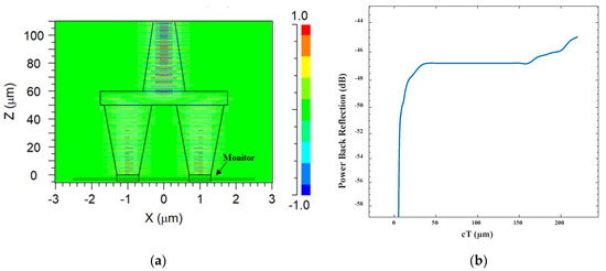
Figure 7.
FDTD simulation setup: (a) schematic sketch of the FDTD setup; (b) the calculation of the back reflection based on FDTD simulation setup.
In our design, reflections could be produced at the boundaries between the cover area and the SiN slab area, and as a side effect of the self-imaging. From the analysis of the FDTD result, the power back reflection was found and its value was 44.94 dB. Figure 7b shows the power back reflection in dB units as a function of cT. The cT is defined as the light propagation direction, which in our case was the z-axis.
As expected, the proposed device did not suffer from the back reflection effect, thus there was no need for a complex MMI coupler design such as an angled MMI coupler to overcome the back reflection losses [15].
To understand and study the advantages of this design, we compared the proposed combiner design to other combiner devices that were previously published. As shown in Table 1, the main characteristics of the power combiners were compared including dimension (length × width), number input of sources (number of sources), operation wavelength band, insertion, loss, and back reflection. It can be seen from Table 1 that the main benefits of the proposed design in this work compared to other combiner devices are the low back reflection and insertion loss. These advantages could be very useful for integrating this combiner into a transmitter system that operated at the O-band spectrum.

Table 1.
Comparison between the main characteristics of different power combiners.
4. Conclusions
In this study, we have shown that it is possible to gain a higher power level using a SiN MMI combiner in a slot waveguide structure. Using the FV-BPM algorithm, it is proven that the SiN MMI coupler can combine two coherent Gaussian laser sources at the operating wavelength of 1310 nm under TE mode polarization with high efficiency, over a light propagation of 109.81 µm. The mode solution shows that TE mode has a large space of 794 nm over the y-axis, which can improve the light coupling between the Gaussian laser source mode and the input waveguide taper modes. The device can function with a high intensity range of 94.8–97.6% of the total power over the O-band range. Thus, this device has good sensitivity to the laser wavelength drift that can happen in transmitter systems that work at the O-band range because of the heating laser process.
This study shows that is not necessarily efficient to use a laser with a higher power level (more than 100 milliwatts) to overcome the power losses that happen because of using a high-speed modulator such as MZM. Instead, it is better to use the proposed power combiner that efficiently combines two standard lasers into one waveguide source with the same level of power of more than 100 milliwatts. Thus, the transmitter system does not need to deal with nonlinear effects that can happen because of using a laser with higher-level power, and the proposed solution is cheaper due to the fact that a complex laser is an expensive cost.
From the results, it is proven that the width and the length of the MMI coupler can overcome large deviations in the dimensions, which makes this coupler very robust for the fabrication process. Furthermore, FDTD was used to show the advance of using SiN slot waveguides and taper waveguides to obtain a very low back reflection of 44.94 dB. Thus, this study can be used for combining two coherent laser sources that function at the O-band and are integrated into a high-speed transmitter system for improving the channel performances. In future research, this study can be utilized to understand how to combine multiple coherent or non-coherent laser sources at the O-band window to obtain a higher level of power in transmitter systems. The problematic issue with non-coherent sources can be dealt with using a phase-shifter or heater, which can be added to the waveguide for solving the phase matching.
Author Contributions
D.M. envisioned the project. D.M. provided guidance. S.K. and N.K. designed the device. S.K. and N.K. performed simulations with the support of D.M. D.M., S.K. and N.K. wrote the paper and the reply letter, S.K. and N.K. made the figures, and all authors reviewed the manuscript. All authors have read and agreed to the published version of the manuscript.
Funding
This research received no external funding.
Conflicts of Interest
The authors declare no conflict of interest.
References
- Kress, B.C. Digital optical elements and technologies (EDO19): Applications to AR/VR/MR. In Digital Optical Technologies; SPIE: Bellingham, WA, USA, 2019; Volume 1106222. [Google Scholar]
- Clémente, J.P. Photonics: A pillar for extended reality technologies. PhotonicsViews 2022, 19, 95–99. [Google Scholar] [CrossRef]
- Kress, B.C.; Chatterjee, I. Waveguide combiners for mixed reality headsets: A nanophotonics design perspective. Nanophotonics 2020, 10, 41–74. [Google Scholar] [CrossRef]
- El-Fiky, S.; Samani, A.; Patel, D.; Jacques, M.; Sowailem, M.; Plant, D.V. 400 Gb/s O-band silicon photonic transmitter for intra-datacenter optical interconnects. Opt. Express 2019, 27, 10258–10268. [Google Scholar] [CrossRef]
- Moshaev, V.; Leibin, Y.; Malka, D. Optimizations of Si PIN diode phase-shifter for controlling MZM quadrature bias point using SOI rib waveguide technology. Opt. Laser Technol. 2021, 138, 106844. [Google Scholar] [CrossRef]
- Cassan, E.; Grillet, C.; Neshev, D.N.; Moss, D.J. Nonlinear integrated photonics. Photonics Res. 2018, 6, NIP1–NIP2. [Google Scholar] [CrossRef]
- Katz, O.; Malka, D. Design of novel SOI 1 × 4 optical power splitter using seven horizontally slotted waveguides. Photonics Nanostruct.-Fundam. Appl. 2017, 25, 9–13. [Google Scholar] [CrossRef]
- Almeida, V.R.; Xu, Q.; Barrios, C.A.; Lipson, M. Guiding and confining light in void nanostructure. Opt. Lett. 2004, 29, 1209–1211. [Google Scholar] [CrossRef]
- Nikolaevsky, L.; Shchori, T.; Malka, D. Modeling a 1 × 8 MMI green light power splitter based on gallium-nitride slot waveguide structure. IEEE Photonics Technol. Lett. 2018, 18, 720–723. [Google Scholar] [CrossRef]
- Xu, Q.; Almeida, V.R.; Panepucci, R.R.; Lipson, M. Experimental demonstration of guiding and confining in nanometer-size low-refractive index material. Opt. Lett. 2004, 29, 1626–1628. [Google Scholar] [CrossRef]
- Malka, D.; Danan, Y.; Ramon, Y.; Zalevsky, Z. A photonic 1 × 4 power splitter based on multimode interference in silicon-gallium-nitride slot waveguide structures. Materials 2016, 9, 516. [Google Scholar] [CrossRef] [Green Version]
- Barrios, C.A. Optical Slot-Waveguide Based Biochemical Sensors. Sensors 2009, 9, 4751. [Google Scholar] [CrossRef]
- Malka, D.; Sintov, Y.; Zalevsky, Z. Design of a 1 × 4 silicon-alumina wavelength demultiplexer based on multimode interference in slot waveguide structures. J. Opt. 2015, 17, 125702. [Google Scholar] [CrossRef]
- Ben Zaken, B.B.; Zanzury, T.; Malka, D. An 8-channel wavelength MMI demultiplexer in slotwaveguide structures. Materials 2016, 9, 881. [Google Scholar] [CrossRef] [Green Version]
- Samoi, E.; Benezra, Y.; Malka, D. An ultracompact 3×1 MMI power-combiner based on Si slot-waveguide structures. Photonics Nanostruct.-Fundam. Appl. 2020, 39, 100780. [Google Scholar] [CrossRef]
- Li, R.; Zhao, Y.; Li, R.; Ge, Y.; Xu, Z. Silicon-on-insulator slot waveguide design for C band optical amplification confinement. Opt. Mater. Express 2021, 11, 1989. [Google Scholar] [CrossRef]
- Soldano, L.B.; Pennings, E.C.M. Optical multimode interference devices based on self-imaging: Principles and applications. J. Lightwave Technol. 1995, 13, 615–627. [Google Scholar] [CrossRef] [Green Version]
- Besse, P.A.; Bachmann, M.; Melchior, H.; Soldano, L.B.; Smit, M.K. Optical bandwidth and fabrication tolerances of multimode interference couplers. J. Lightwave Technol. 1994, 12, 1001–1009. [Google Scholar] [CrossRef] [Green Version]
- Fujisawa, T.; Koshiba, M. Theoretical Investigion of ultrasmall polarization-insensitive multimode interference waveguide based on sandwiched structures. IEEE Photonics Technol. Lett. 2006, 18, 1246–1248. [Google Scholar] [CrossRef]
- Xu, C.; Hong, X.; Huang, W.P. Design optimization of integrated BiDi triplexer optical filter based on planar lightwave circuit. Opt. Express 2006, 14, 4675–4686. [Google Scholar] [CrossRef]
- Irace, A.; Breglio, G. All-silicon optical temperature sensor based on Multi-Mode Interference. Opt. Express 2003, 11, 2807–2812. [Google Scholar] [CrossRef]
- Zhang, Y.; Liu, L.; Wu, X.; Xu, L. Splitting-on-demand optical power splitters using multimode interference (MMI) waveguide with programmed modulations. Opt. Commun. 2008, 281, 426–432. [Google Scholar] [CrossRef]
- Hosseini, A.; Kwong, D.N.; Zhang, Y.; Subbaraman, H.; Xu, X.; Chen, R.T. 1xN Multimode Interference Beam Splitter Design Techniques for on-Chip Optical Interconnections. J. Lightwave Technol. 2011, 17, 510–514. [Google Scholar]
- Tajaldini, M.; Jafri, M.Z.M. Ultracompact Multimode Interference Coupler Designed by Parallel Particle Swarm Optimization with Parallel Finite-Difference Time-Domain. J. Lightwave Technol. 2014, 32, 1282–1289. [Google Scholar] [CrossRef]
- Blanch, P.A. Holographic Combiners Improve Head-Up Displays. Photonics Media 2019, 53, 34–37. [Google Scholar]
- Sharma, A.; Goswami, K.; Mondal, H.; Datta, T.; Sen, M. A review on photonic crystal based all-optical logic decoder: Linear and nonlinear perspectives. Opt. Quantum Electron. 2022, 54, 54–90. [Google Scholar] [CrossRef]
- Kimmel, J.; Levola, T.; Saarikko, P.; Bergquist, J. A novel diffractive backlight concept for mobile displays. J. Soc. Inf. Disp. 2008, 16, 351–357. [Google Scholar] [CrossRef]
- Melloni, A.; Costa, R.; Monguzzi, P.; Martinelli, M. Ring-resonator filters in silicon oxynitride technology for dense wavelength-division multiplexing systems. Opt. Lett. 2003, 28, 1567–1569. [Google Scholar] [CrossRef]
- D’Orazio, A.; De Sario, M.; Petruzzelli, V.; Prudenzano, F. Photonic band gap filter for wavelength division multiplexer. Opt. Express 2003, 11, 230–239. [Google Scholar] [CrossRef]
- Dragone, C.; Strasser, T.; Bogert, G.A.; Stulz, L.W.; Chou, P. Waveguide grating router with maximally flat passband produced by spatial filtering. Electron. Lett. 1997, 33, 1312–1314. [Google Scholar] [CrossRef]
- Taubenblatt, M.A. Optical interconnects for high-performance computing. J. Lightwave Technol. 2012, 30, 448–457. [Google Scholar] [CrossRef]
- Thomson, D.; Zilkie, A.; Bowers, J.E.; Komljenovic, T.; Reed, G.T.; Vivien, L.; Morini, D.M.; Cassan, E.; Virot, L.; Fédéli, J.M.; et al. Roadmap on silicon photonics. J. Opt. 2016, 18, 07300310-1088. [Google Scholar] [CrossRef]
- Pantouvaki, M.; Srinivasan, S.A.; Ban, Y.; De Heyn, P.; Verheyen, P.; Lepage, G.; Chen, H.; De Coster, J.; Golshani, N.; Balakrishnan, S.; et al. Active components for 50 Gb/s NRZ-OOK optical interconnects in a silicon photonics platform. J. Lightwave Technol. 2017, 35, 631–638. [Google Scholar] [CrossRef]
- Blumenthal, D.J.; Heideman, R.; Geuzebroek, D.; Leinse, A.; Roeloffzen, C. Silicon Nitride in Silicon Photonics. Proc. IEEE 2018, 106, 2209–2231. [Google Scholar] [CrossRef] [Green Version]
- Mu, J.; Vázquez-Córdova, S.A.; Sefunc, M.A.; Yong, Y.; García-Blanco, S.M. A Low-Loss and Broadband MMI-Based Multi/Demultiplexer in Si3N4/SiO2 Technology. J. Lightwave Technol. 2016, 34, 3603–3609. [Google Scholar] [CrossRef]
- Bucio, T.D.; Khokhar, A.Z.; Mashanovich, G.Z.; Gardes, F.Y. N-rich silicon nitride angled MMI for coarse wavelength division (de)multiplexing in the O-band. Opt. Lett. 2018, 43, 1251–1254. [Google Scholar] [CrossRef]
- Melloni, A.; Costa, R.; Cusmai, G.; Morichetti, F.; Martinelli, M. Waveguide index contrast: Implications for passive integrated optical components. In Proceedings of the 2005 IEEE/LEOS Workshop on Fibres and Optical Passive Components, Mondello, Italy, 22–24 June 2005; pp. 246–253. [Google Scholar]
- Burns, W.K.; Milton, A.F.; Lee, A.B. Optical waveguide parabolic coupling horns. Appl. Phys. Lett. 1977, 30, 28–30. [Google Scholar] [CrossRef]
- Milton, A.; Burns, W. Mode coupling in optical waveguide horns. IEEE J. Quantum Electron. 1977, 13, 828–835. [Google Scholar] [CrossRef]
- Kojima, K.; Akino, T.K. Novel multimode interference devices for wavelength beam splitting/combining. In Proceedings of the 2015 International Conference on Photonics in Switching (PS), Florence, Italy, 22–25 September 2015; pp. 34–36. [Google Scholar]
Publisher’s Note: MDPI stays neutral with regard to jurisdictional claims in published maps and institutional affiliations. |
© 2022 by the authors. Licensee MDPI, Basel, Switzerland. This article is an open access article distributed under the terms and conditions of the Creative Commons Attribution (CC BY) license (https://creativecommons.org/licenses/by/4.0/).