1. Introduction
Battery-powered electronics systems, such as wearable and mobile devices, wireless sensors, and medical devices are widely used during the everyday life. Implantable medical devices (IMDs) represent a category of electronic systems which have an increasing impact in the improvement of quality of life since they enable monitoring or replacing of sensory functions. The idea of using an IMD to assist patients originates since 1950s when the appearance of transistors opened the possibility of implementing a fully implantable pacemakers [
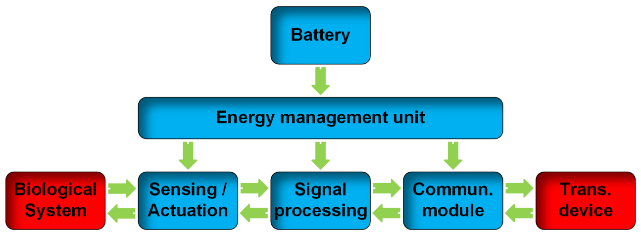
1]. From that, various devices have been developed such as heart rate monitors, cochlear implants, retinal implants and brain-computer interfaces. All these devices have a similar architecture which is summarized in
Figure 1.
It comprises circuital blocks for sensing/actuation, signal processing, communication (transmitter device), and energy management as well as for energy storage (usually implemented by a battery). Although the power required by an IMD is contained, the methods to provide energy to these kind of electronic devices represent the bottleneck of their diffusion. Indeed, the technological progress of batteries does not have a similar trend of the semiconductor transistors scaling, therefore devices are much smaller than the battery needed for their operation, limiting the minimum volume of the implanted device. The pacemakers, for instance, clearly demonstrate such limitation considering that their total volume, dominated by the battery, has hardly changed over decades of evolution. Thus, for implantable devices, the battery is not suitable for its invasive dimensions and its limited lifetime. Moreover, batteries require a new surgery operation for replacement or need to be recharged by wireless system [
1,
2].
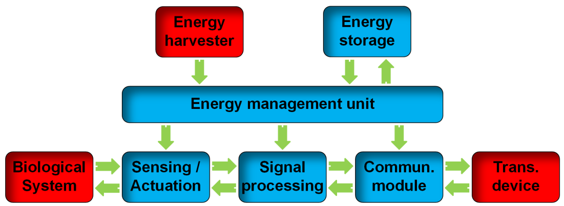
To solve these issues, the idea of recovering energy from the environment is adopted. A system exploiting this technique, usually referred to in the literature as energy harvesting, is shown in
Figure 2. The energy recovered from light, vibrations or temperature gradients, allows extending the system lifetime by reducing the battery capacity or even eliminating it [
3,
4,
5,
6,
7,
8,
9,
10]. Battery-less systems allows longer and potentially unlimited lifetime, reduced size, improved bio-compatibility and better eco-friendliness. However, an IMD based on energy harvesting still requires an energy storage device to be used to enable the systems working even when no energy can be collected from the energy harvester. In this case, direct connection between the energy harvester and the energy storage device is usually not possible and the energy management unit is in charge of handling its charging/discharging. For this purpose, simple capacitors are preferred over batteries due to their superiority in terms of life cycle and compactness.
The methods of providing power to IMDs can be categorized into two types, namely the
in-body type and the
out-of-body type. The in-body energy sources come from the human body. Some examples are vibrations gathered from patient movements, breathing activity, and heartbeats through piezoelectric devices, or temperature gradients between the inner body, the skin and the air that are converted into voltage by thermo-electric generators (TEGs) [
11,
12,
13]. Unfortunately, these in-body sources provide extremely low and unpredictable power levels which prevent their adoption in most applications [
14,
15,
16]. In out-of-body power delivery, an external energy source is coupled to the energy harvester implanted inside the body, which will charge an accumulation device (rechargeable battery or, more frequently, a capacitor) or will directly feed the IMDs [
5,
17]. The external power can be provided through radiofrequency, electromagnetic induction or Ultrasound (US) waves. Among these power transfer systems, only US waves have the capability to enable simultaneous power and data transfer in deep-implanted (>2 cm) mm-sized devices [
18,
19,
20,
21]. Indeed, the spatial-peak temporal-average intensity (or ISPTA) allowed by American Food and Drug Administration is 7.2 mW/mm
for diagnostic US applications, while the exposure limit for Electro-Magnetic (EM) systems, set by the Federal Communications Commission and IEEE, is only 10–100 μW/mm
[
22]. As a result, about two orders of magnitude higher power can be transmitted using US, which is particularly useful for deep IMDs. Moreover, because acoustic waves do not directly interact with EM waves, they are not as susceptible to EM interference nor do they significantly affect the EM fields of the surroundings. Finally, US waves have smaller wavelengths in tissue (e.g., ∼1.5 mm at 1 MHz) and low tissue attenuation (∼0.5–1 dB/cm/MHz) allowing highly directive focusing down to millimeter spots at great depths and high acoustic-electrical efficiency with sub-millimeter-sized receivers [
19,
23]. The adoption of US energy harvesting systems relies on piezoelectric devices.
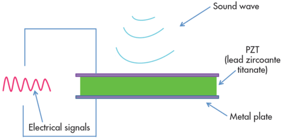
The piezoelectric phenomenon was discovered in 1880 by the French physicists Jacques and Pierre Curie [
24]. They discovered that certain materials generate an electrical polarization proportional to an applied mechanical stress via the piezoelectric effect (
Figure 3).
When an external force is applied, positive and negative charged surfaces are generated, called polar surfaces. The piezoelectric potential created by these polar surfaces can be used to drive electrons in an external circuit, realizing the conversion of mechanical energy into electricity. During the operations of the piezoelectric devices, polar surfaces have to be maintained in order to generate continuously the electric energy. At this purpose, US waves are the widely used means to induce a stress on the piezoelectric material. Thus, the output voltage of a piezoelectric transducer results to be an AC voltage. The frequency of the US wave is set equal to the resonant frequency of the transducer, which is inversely proportional to its size.
As mentioned above, from an electrical point of view a piezoelectric device generates an AC voltage. Therefore, a system that provides AC–DC conversion is required to provide a DC supply to the electronic systems of the IMD. At the same time, due to possible misalignment between the external generator and internal transducer, the amplitude of the output voltage could unpredictably vary and, consequently, it is not suitable to directly feed the circuits.
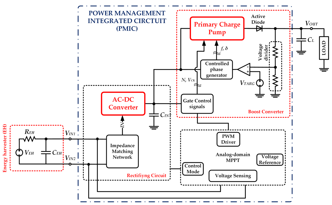
As shown in
Figure 4, a typical power management integrated circuit (PMIC) consists of an AC–DC converter and a power converter, whose output voltage is controlled to provide a specific DC voltage value. Since the piezoelectric devices are often chosen from those commercially available, the architecture of the PMIC is the main diversification factor among the various proposed IMDs. In decades of evolution, the PMIC topology has been made more complex to meet the more and more stringent specifications imposed by device miniaturizations and ultra-low-power constraints.
The output voltage of the rectifier is always less than the maximum input voltage, therefore, it may be too low to supply any electronics system. To solve this problem a boost converter is necessary. The DC-DC boost converter in
Figure 4 can be implemented using switched inductor (SI) or switched capacitor (SC) topologies. SI converters are suitable for applications requiring high power but requires bulky off-chip components (inductors and/or transformers), resulting in a cost increase of the entire system. Moreover, magnetic components strongly reduces scalability and compactness of the IMD, making it unsuitable for applications requiring minimal invasive systems with mm-scale form factor [
25]. On the other hand, in low-power low-area applications, SC converters represents a better alternative since they are amenable for full on-chip integration SC converters with a voltage gain higher than one are referred to in the literature as voltage multipliers or charge pumps (CPs) [
6,
26,
27,
28]. The conventional topologies of a monolithic charge pumps are the linear known as Dickson and Cockcroft-Walton charge pumps, which are made up of MOSFET diodes and capacitors clocked by a two-phases clock generator. In these topologies, an increase of the output power requires an increase of the capacitance value of each stage. Thus, new schemes, aimed to reduce the silicon area which occupy and improve their power efficiency, are continuously studied and introduced in the literature [
6].
With this in mind, this paper is aimed to provide a deep-insight of energy harvesting systems from US waves targeted to feed IMDs. This is allowed by analyzing the design constraints and basic topologies used to satisfy the specifications required by application, and reviewing the state-of-the-art. The work is organized as follows. The second section gives information about the operation principle and topology of the conventional circuits used to rectify the AC signal outputted by the piezoelectric device. In the third section, the state-of-the-art of the PMICs for IMDs is reviewed and performance comparison is reported in section four. Finally, some conclusions close the paper.
2. Conventional Topologies for AC–DC Conversion
As mentioned above, the systems of interest harvest energy by means of a piezoelectric transducer, which converts ultrasound (US) waves into alternate electrical quantities, voltage and current. For medical devices, Food and Drug Administration (FDA) limits for power transmission into tissue to be the U.S. lesser than 7.2 mW/mm. Therefore, with the compact size requirements, power induced by US sources results to be limited in the order of few milliWatts. Typically, attenuations due to the US link (in this case, human tissues) further decreases these values. Thus, the system requires a very efficient conversion from AC to a DC voltage and a regulator to supply the biomedical functional circuits.
To convert the AC voltage into a DC voltage a circuit (called
rectifier) is required. The basic elements of a rectifier are
diodes, historically realized with PN junctions, but they can also be implemented by using transistors (i.e., diode-connected transistors, PMOS diodes and NMOS diodes). These diodes are made by connecting gate and drain of the transistor and the current flows as indicated by the arrow. This type of diode may exhibit a relatively high leakage current when realized by means of a short-channel transistor, therefore, to reduce the reverse leakage, a composite CMOS diode can be adopted [
29]. Nonetheless, this topology increases the conduction resistance which in turn increases the forward dropout voltage. The choice of a specific diode is mainly driven by the characteristics of the adopted technology, the minimum amplitude of the input signal and realization costs. However, the MOS-based diode, in its simple or composite version, seems to be a valid trade-off in many cases and it is the widely adopted device in AC–DC converters.
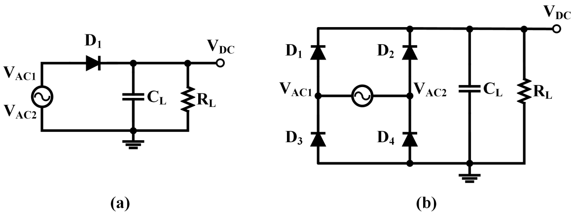
The main rectifier topologies are classified as passive and active rectifiers. In passive rectifiers, the transistors work as simple diodes while in active rectifiers, auxiliary circuits are added to decrease the voltage drop and improve the performance of the transistors used as diodes. Two traditional passive rectifier topologies are shown in
Figure 5 [
29].
Focusing on
Figure 5a, in the first half cycle
is positive and the diode
will conduct when
goes higher than the DC output voltage
. During the second half cycle
is negative and
is surely reverse-biased. Therefore, this circuit delivers current from the AC source to the DC output, at the maximum, during a half cycle, therefore it is called
half-wave rectifier.
On the other hand, in the rectifier shown in
Figure 5b, during the first half cycle, the diodes
and
will conduct when
is higher than
. In next half cycle,
and
will conduct when the voltage
is higher than
. Therefore, this circuit delivers current to the output twice a cycle, it is so-called
full-wave rectifier. These solutions of rectifiers are very simple but have high dropout voltage and require an input voltage greater than one or two threshold voltage. Another passive rectifier is the
Cross Coupled topology, whose simplified diagram is shown in
Figure 6 [
29].
The cross-coupled rectifier is widely used for its low-voltage and auto-switching characteristics. For high input voltage , the MOS transistors will act as switches with low on-resistance for rectification, and the forward voltage drop is minimized. However, a high leakage current may occur if the input voltage, during the transition instants, is too high because the PMOS and NMOS will be turned on simultaneously short-circuiting the two supply rails. This rectifier operates efficiently with low input voltage, also below the threshold voltage level. In such case, reverse and short-circuit currents are extremely reduced, but the on-resistance is increased, making the rectifier useful for very-low power applications (e.g., sub-μW power level). If the input voltage is larger than the threshold voltage of the transistors, the leakage current becomes relevant and the efficiency decreases, but the channel becomes more conductive decreasing the on-resistance and enabling mW -power level operations.
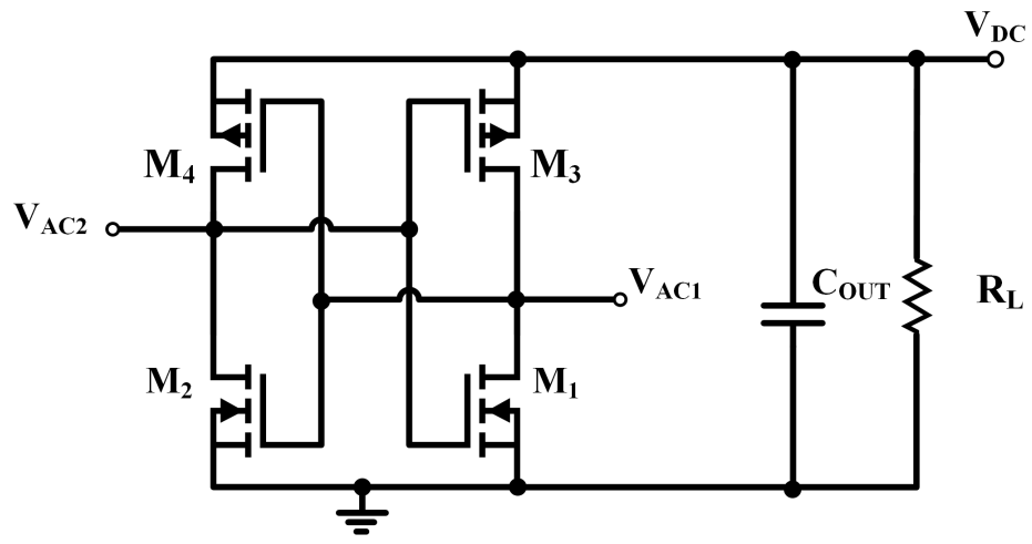
The active rectifier shown in
Figure 7 has the same structure of the passive full-wave rectifier but diodes are replaced by
active-diodes.
Active diodes are essentially comparator-controlled MOSFETs. The operation principle of the active full-wave rectifier can be described as follows. Let us assume that the process starts with going down and going up. When (threshold voltage of M), M is turned on and therefore . Then swings below the ground voltage, the comparator CMP1 turns on the switch M, and charges up through the AC source. When swings above zero, M is then turned off by CMP1, finishing one half cycle of the full-wave rectification period. During the next half of the AC input cycle, the other half of the rectification circuit will conduct in a similar manner as described above. Active diodes do not exhibit the large forward dropout voltage of conventional diodes and prevent the reverse leakage current. However, the implementation of an active diode entails additional area and power consumption for comparators. Moreover, they suffer in start-up at low input voltage because, generally, the comparator is powered by the output voltage of the rectifier.
As already mentioned, the output voltage of the transducer or the rectifier may be too low to directly supply any electronics system. A possible solution is to exploit blocks which boost the voltage to the needed level (e.g., voltage multipliers or charge pumps). Such circuit can constitute a different building block of the conversion chain or replace the rectifier, acting as AC–DC boost converter [
8,
30,
31].
Figure 8 shows the simplified schemes of the most used charge pump circuits.
As with the rectifier topologies, diodes are often replaced by MOS-based passive and active diodes [
6]. Signals which clock the circuit, named
and
in the figure, can be generated internally the IMDs, for example by using a controlled oscillator, or can be provided directly by the transducer. In the first case, the Dickson CP is the topology widely adopted and it acts as DC-DC boost convert, moreover, in order to decrease the capacitance value of the pumping capacitor,
C, and improve the PCE, high frequency counter-phase square-wave signals are used. In the second case, where the frequency of the clock signal is imposed by the adopted piezoelectric transducer, the widest adopted is Cockcroft-Walton CP, and it implements the AC–DC conversion.
It is worth noting that also the cross-coupled structure can be exploited to realize diodes for CPs [
32,
33]. They are essentially latch-configured inverters with
similar to the dual-branch charge pumps [
6], but the pumping capacitances of a single stage are halved. These dual compensated structures introduce many benefits akin to the dual-branch structures. It improves pumping efficiency and reduces ripples in the output voltage. Moreover, while in a Dickson CP the voltage drop across each switch is equal to the diode threshold voltage,
, in the cross coupled charge pump the voltage drop is equal to the drain-to-source voltage
, which is lower than
. The output voltage of the charge pump depends on the power required by the load, therefore this voltage can be change dynamically. To prevent changes in this voltage, some type of feedback control can be implemented. The principal control technique based on frequency modulation, pulse width modulation and amplitude modulation of clock signal, are deeply analyzed in [
8].
3. The State-of-the-Art of AC–DC Converters
Many solutions have been proposed in the literature to improve the performance of the PMIC for IMDs. Since the output voltage of the transducer is an AC signal whose frequency ranges from some kHz to about 30 MHz [
5], AC–DC converters topologies exploited for radiofrequency energy harvesting within low frequency range (e.g., below 100 MHz) could be adopted. For this reason, in this review some works based on radiofrequency energy harvesting are also included. Moreover, although all the solutions analyzed in this paper are equally interesting, for the sake of of conciseness only the topologies suitable for ultrasound energy harvesting are considered.
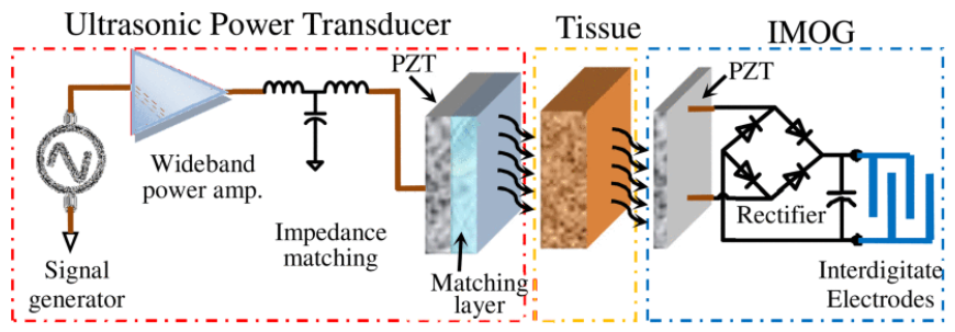
As a first example, Maleki et al., in [
34], presented an ultrasonically powered implantable micro-oxygen generator (IMOG) that is capable of in situ tumor oxygenation through water electrolysis. Wireless ultrasonic powering (2.15 MHz) was employed to increase the penetration depth and eliminate the directional sensitivity associated with magnetic methods. The block diagram of the overall system is shown in
Figure 9. In this case the receiver is constituted of a passive full-wave rectifier, a filter and the interdigitated electrodes which act as micro-oxygen generator. Although an output voltage up to 6.4 V and an output current equal to 300 μA is reported [
34], the system performance is limited mainly by the passive rectifier.
Huang et al. proposed a generic rectifier system for biomedical implants [
35]. As shown in
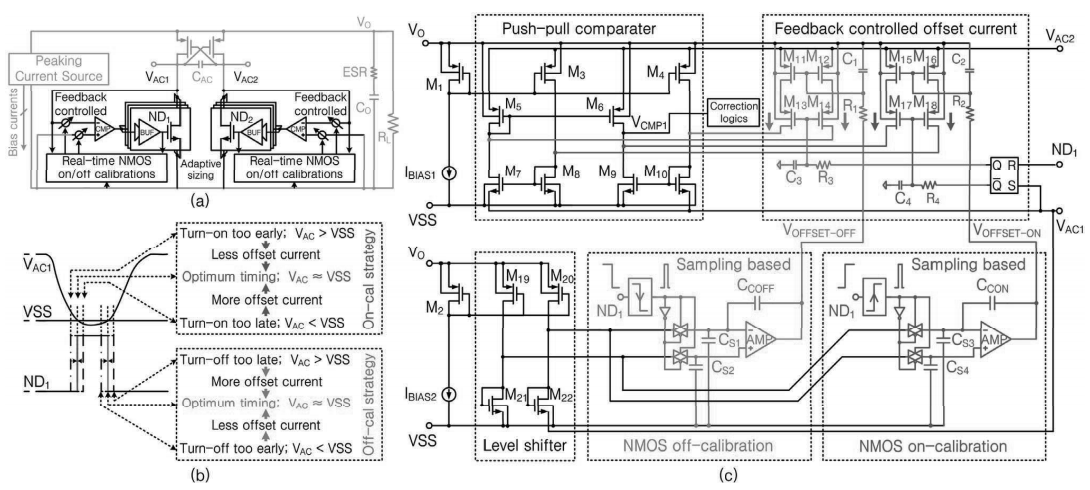
Figure 10, the full-wave rectifier is composed of two cross-coupled PMOS and two active NMOS-diodes. As compared to the classic topology, it implements a real-time NMOS on/off calibration to make sure the rectifier always operates at near-optimum conditions with circuit-delay elimination under different (process, voltage and temperature) corners and loading conditions, thus both power conversion efficiency (
) and voltage conversion ratio (
) are significantly improved. Moreover, NMOS adaptive sizing is also introduced for
optimization over a wide loading range. However, this system operates at 13.56 MHz and requires a relatively high input voltage (from 1.2 V to 2.4 V).
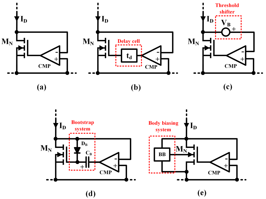
It is worth noting that a lot of solutions proposed in the literature adopt AC–DC with at the least one couple of active diodes, NMOS- or PMOS-type, because they allow heavily reducing reverse and short-circuit current losses, which are the main drawbacks of the conventional cross-coupled structure (i.e., currents flowing from the output to the ground when transistors are switched-off or switched-on simultaneously). Improved versions of active diodes have been continuously introduced with the aim of further increasing the power efficiency of the whole converter. Generally three aspects, namely turn-on instant, conduction angle and MOSFET channel conductivity, mainly affect the .
Turn-on instant, defined as the time when the active diode is turned-on, can affect cross-conduction of MOSFETs constituting a single leg (for instance, transistors M
and M
or, alternately, M
and M
, which constitute a vertical section of
Figure 7). This time must be calibrated in order to avoid any time slot where transistors of the same leg are on simultaneously. In a simple implementation, it is sufficient to make sure that the active diode switches when the complementary MOSFET is cut-off. Contextually, conduction angle, defined by the effective angular portion of input signal which is converted, has to be maintained as wide as possible to preserve the highest power transferring. Therefore, solutions on this way can be categorized based on the adopted strategy to modulate turn-on instant and conduction angle. As an example, some works introduced architectures where auxiliary delay cells are inserted with the aim to adjust the times when the MOSFET have to switch from cut-off to conduction, and vice-versa [
36]. Similar effect can be obtained by acting on the effective threshold of the comparator. This can be done adding a voltage generator in series with one of the input terminals or designing the inner differential couple in an asymmetrical way. Among the topologies that exploit these design strategies, there are those presented in [
37,
38,
39].
On the other hand, modulation of the channel conductivity can be an effective strategy to pursuit for those applications whose input signal amplitude is lower than a conventional threshold voltage (about 600 mV). Bootstrapping of the gate terminal and/or body biasing techniques are often exploited to control the channel conductivity of interested MOSFETs. Both strategies act similarly on the electrical features of the MOSFET, and they can be used to improve the conduction and/or to reduce reverse losses [
40,
41,
42]. Simplified block diagrams of the architectural solutions just mentioned, are gathered in
Figure 11.
In [
31], it is shown as AC–DC charge pump circuits can be optimally designed to have the minimum circuit area for small form factor vibration energy harvesting. The proposed system (
Figure 12) was composed by a passive cross-coupled AC–DC converter without filter, whose rectified output signal feeds a current-controlled ring oscillator and a Dickson CP, whose diodes were implemented by composite CMOS diodes. The frequency of the clock signals was higher than that of the input signal, in such manner pumping capacitances can be reduced and output current strongly increased as respect to the CPs for AC–DC conversion present in the literature.
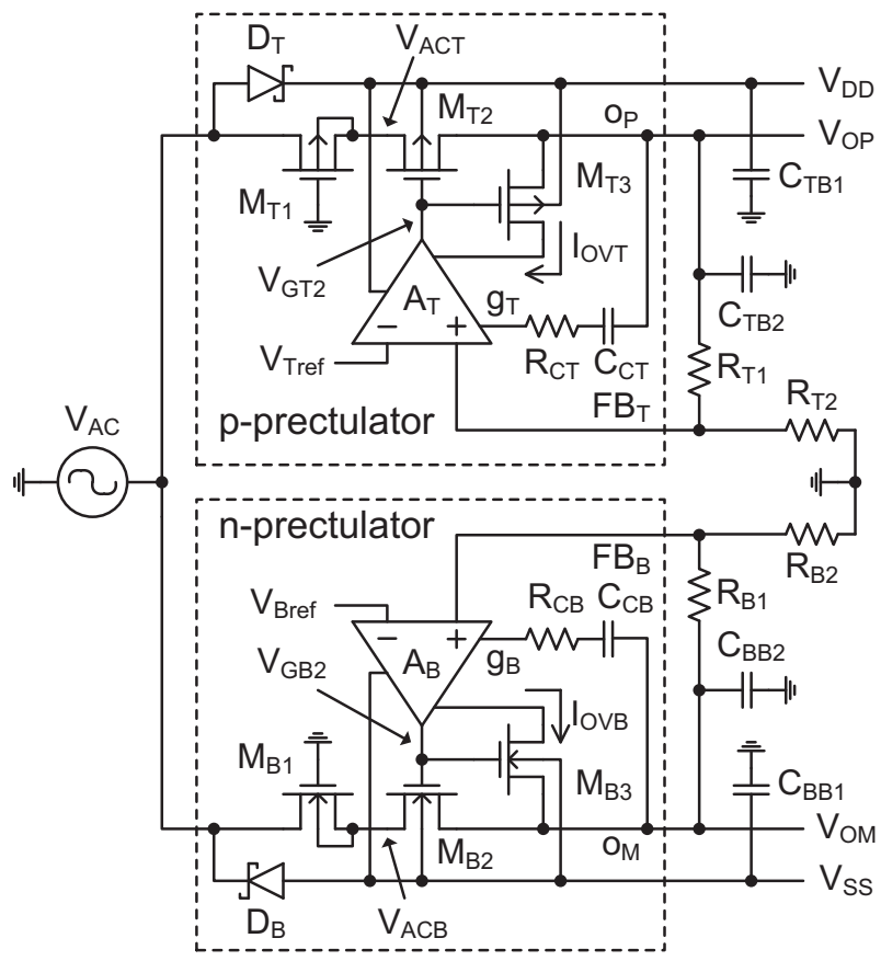
Lee proposed a technique that combines a passive rectifier and a linear regulator without using a comparator (named
prectulator) [
43]. Since there is no speed limitation due to the comparator, the proposed technique can operate with high frequency input signals. As can be seen in
Figure 13, the output transistor used for regulating the output voltage in a linear regulator is also used as a passive rectifier. To achieve rectification without turning on the parasitic bipolar transistor of the output transistor, an auxiliary rectifier is used for biasing the bulk terminal of the output transistor.
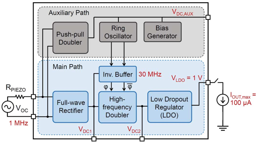
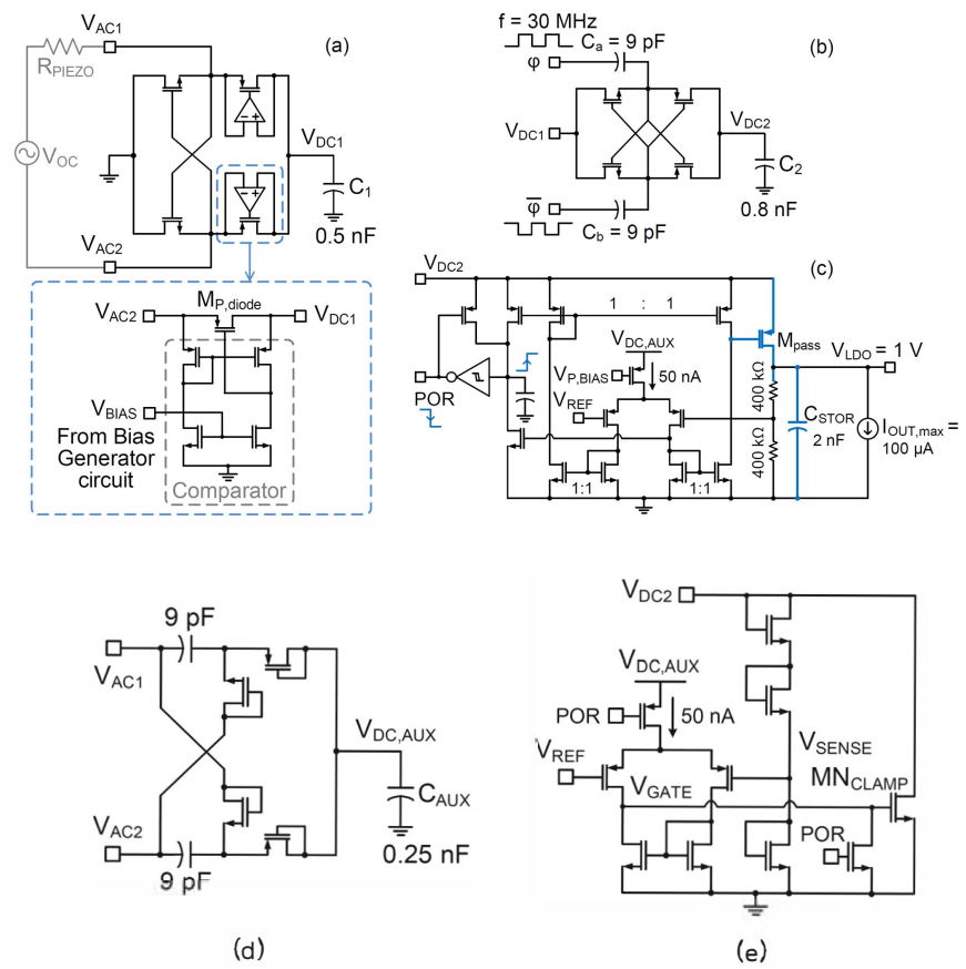
An implantable system for powering and data transmission is proposed in [
44] (
Figure 14). This system employs two rectifier paths, namely the main and the auxiliary path. In the main path there are the main rectifier (
Figure 15a), DC-DC cross coupled Dickson charge pump (
Figure 15b) and a regulator (
Figure 15c). The main rectifier is realized by cross coupled NMOS and active PMOS diode with a simple comparator. The auxiliary path is used to supply a ring oscillator and a bias generator circuit. The use of a ring oscillator allows working at high frequency thus reducing the size of the capacitors. The rectifier of the auxiliary path is a push-pull voltage doubler (
Figure 15d). For high available input power,
for this architecture increases with
. For low available input power,
is low, resulting in lower rectification efficiency because
is limited by the quiescent power dissipation in the LDO and other circuit blocks.
In [
45], a PMIC is presented that adopts a full-wave CMOS rectifier (NMOS active diode and cross-coupled PMOS) to convert AC to DC voltage and a newly developed multi-ratio switched-capacitor DC-DC regulator to provide a regulated output voltage. However, this solution works on an input voltage range of 1.9 V to 3.5 V.
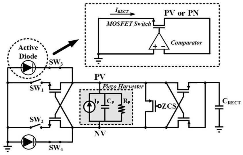
The solution proposed in [
46] consists of the dual-mode rectifier, shown in
Figure 16, to work well on wide range of input AC voltage and many blocks to improve PCE. This topology solves the problem during start-up and for low input power with a cross-coupled passive rectifier for high input power an active diode rectifier is used.
The system works for a wide range of input voltage, with a minimum value equal to 1 V. However, the large number of ancillary blocks need additional input power.
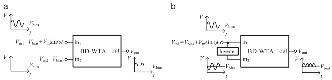
In [
47], it is presented a half/full wave rectifier (
Figure 17) based on a maximum selector, which is based on bulk-driven comparator. This technique is very low-power, nevertheless it works under several ten of kilohertz.
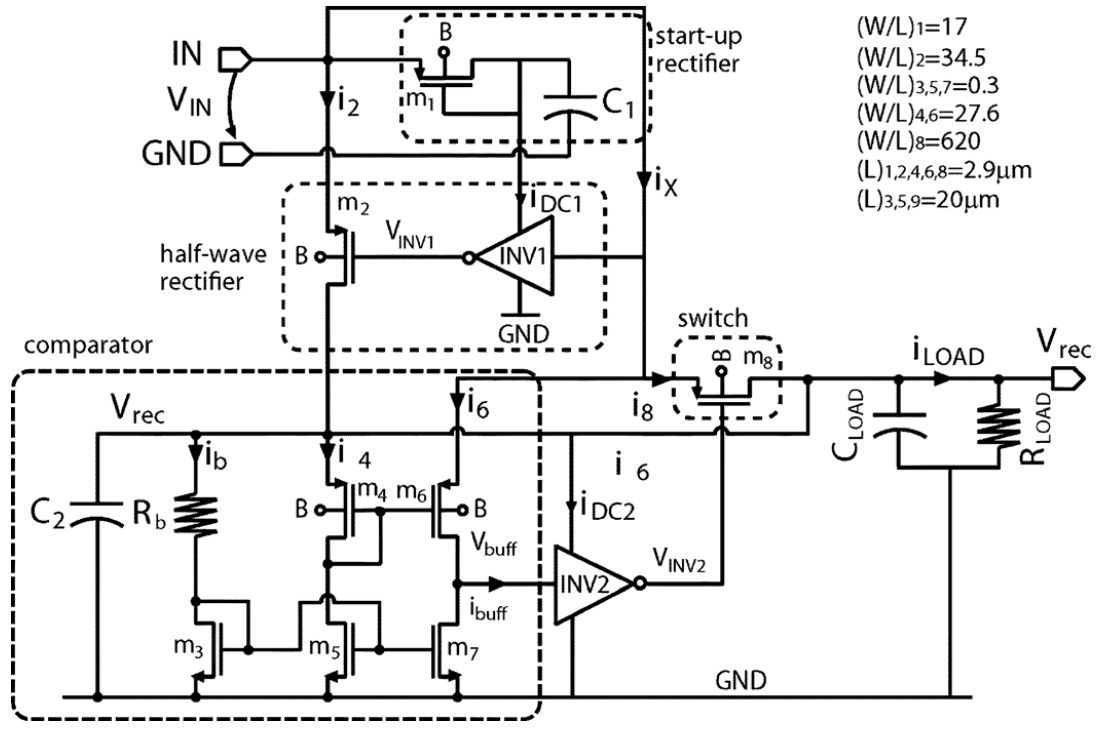
A half-wave active rectifier is proposed in [
48].
Figure 18 shows the circuit diagram of the single-stage half-wave active rectifier made up of a start-up rectifier, a half-wave rectifier, a comparator, a buffer and a power switch.
The active rectifiers exploit a fast comparator to directly control the gate of PMOS transistors to reduce reverse current leakage from the output load to the input. In standard cross-coupled topology, full-wave input voltage is applied between the gate and source of all transistors. Consequently, PMOS and NMOS transistors will turn on/off roughly at the same time which creates a leakage path from load to source. To prevent leakage currents rectifier should only turn on when the input voltage is higher than the load voltage. For this reason, ref. [
41] proposes a rectifier topology (
Figure 19) where the turn on/off voltage level of rectifier is controlled by applying independent bias voltage to the NMOS transistors. At the same time, this solution requires high-input voltage (from 1.6 V to 3.6 V).
Work in [
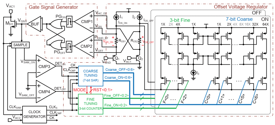
49] presents an active rectifier with SAR-assisted coarse-fine adaptive digital delay compensation technique for biomedical implantable devices. Both on- and off-delay are compensated by adjusting the comparator offset. In order to achieve accurate zero-voltage switching against process, voltage, and temperature variations (PVT), a two-step coarse-fine digital tuning method is introduced.
The architecture of adaptive digital on/off delay compensation loop for the power switch M
is shown in
Figure 20. The loop consists of a sampled block, a detection circuit, an offset regulator and a gate signal generator. This solution could avoid reverse current and achieve maximum conduction time for power switches.
The rectifier proposed in [
50], whose scheme is depicted in
Figure 21, consists of a CMOS passive rectifier with active bias tuning (ABT), allowing a widely extended input range with high power conversion efficiency.
The ABT is a digital circuit which has two functions: maintain high
and regulate V
by searching (
Figure 22). In particular, in closed-loop the control senses V
and compare it with its previous value. The comparison result directs a finite-state machine (FSM) to signal either “charge” or “discharge” to the switched-capacitor charge pump. This solution is only convenient if several cross-coupled structures are cascaded. In fact, measurement results of three chips show that this rectifier improves the
over a wide input range, with a maximum value equal to 64.4%.
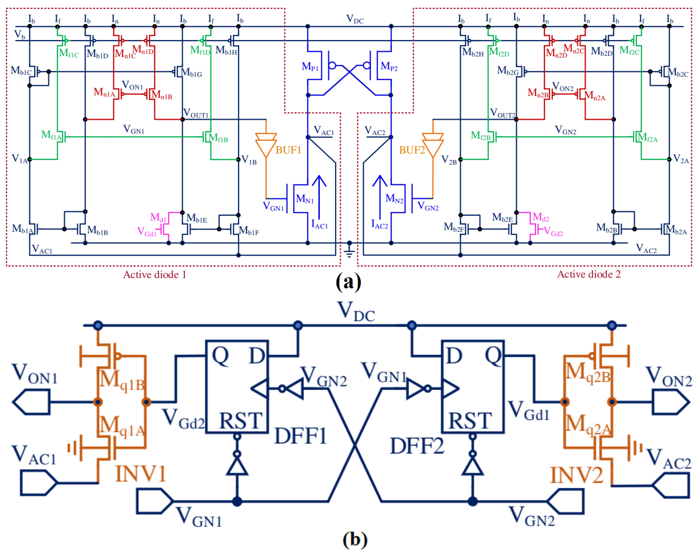
An active rectifier with digitally controlled on-off delay-compensated for biomedical application is introduced in [
51]. It consists of two NMOS active diodes and a cross-coupled PMOS transistor-pair (
Figure 23). High efficiency is achieved by digital techniques that eliminate turn-on delay, reverse current and multiple pulsing.
4. Performance Comparison
The choice of a specific rectifier topology depends upon the specific application, the used technology, and design specifications. The choice of a specific rectifier topology can be firstly done according to the input voltage range, as suggested in the following.
In ultra-low input voltage range (0.1–0.6 V) applications, such as micro-scale and battery-less biomedical implants, body driven circuits represent a good option because the threshold voltage of transistor is often relatively high and body driven topologies overcome this problem. Moreover, boost converters are often mandatory to adapt the rectified voltage at the levels conventionally required for functional block operations.
For low input voltage range (0.6–1.2 V) applications, passive rectifiers, such as cross-coupled and voltage doubler, are a good choice because the transistors work sufficiently well without additional circuits (that would reduce the ).
For mid and high input voltage range (higher than 1.2 V) applications, active rectifier topologies represent the best choice to optimize its performance in terms of power consumption (i.e., ).
The solutions for implanted medical devices previously analyzed are compared in
Table 1. Please note that the data shown in the table do not refer only to the adopted rectifier but to the overall PMIC. In
Table 1,
and
are respectively defined as
where
is the averaged rectified output DC voltage,
is the output resistive load,
T is the period of the input sinusoidal signal,
is the integration range over
is calculated, and
,
are the instantaneous voltage and current of the AC input source,
and
are the actual and ideal output voltage of the system.
Analysis of data reported in
Table 1 reveals that the body driven rectifier proposed in [
47] is the only solution for ultra-low input voltage range. However, such result was accomplished because the proposed BD-WTA is supplied by an auxiliary power source whose voltage is higher than the input signal amplitude. Actually, the circuit works as comparator where the resulting output voltage is always the maximum between the two inputted signals. Main drawbacks and limits of this circuit are strictly related to the needed of auxiliary supply and biasing sources and the use of the body-driven approach which allows working on very-low voltage input signals but limits their maximum amplitude values. Definetively, comparator in [
47] is particularly suited as envelope detector for applications where the input signal amplitude contains information to be extracted, such as amplitude modulation receiver.
On the other hand, the features of [
44] confirm that active topologies are not suitable for low input voltage range since they have
. Reasons of the relatively low power performance can be found in the loss of speed and driving capability of the auxiliaries, such as comparators and bias generators, when the transistors are constricted to work in sub-threshold region. This confirms the categorization done before, since typical values for the threshold voltage of a regular MOSFET is about 600 mV.
The analysis of solutions in [
35,
41,
45,
48,
49,
50,
51] further confirm the validity of the guidelines provided above, suggesting that mixed approaches are needed to extend the input voltage range. As a proof, the mixed rectifier, constituted by cross-coupled and active diode proposed in [
46] allows functions in a wide input voltage range due to the adaptive configuration of the rectifier.
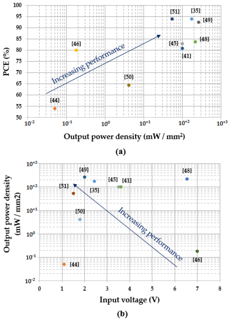
Figure 24a reports
versus the maximum output power density, defined as the ratio between the maximum output power and area occupation for all the solutions in
Table 1. It is apparent that [
51] shows the best performance due to the higher value of
and output power density, while occupying much more area than [
45]. High power efficiency of solution in [
51] is reached thanks to an on-off delay compensation implemented through a digital control circuit. As claimed by the authors, Pal et al., the comparator and logic losses affects the total power breakdown for less than 1%, allowing obtaining a reduction of the losses, associated to rectifier, limited in the range of some percentile points. The achieved results prove that the use of digital-based circuitry to control switching activity of the active diodes is a captivating solution for high-power super-threshold IMD applications.
Figure 24b shows the maximum output power density versus the input voltage. By inspection of this figure, it is apparent that the solution reported in [
46] achieves a low value of maximum supply voltage (1.1 V) but it has the lowest output power density. Consequently, its performance is lower than [
35,
49,
51]. The best performance is therefore achieved by the solutions proposed in [
35,
49,
51].
5. Conclusions
In this work, a review of several solutions of ultrasound-based energy harvesters for implantable devices is presented. After a general presentation of the widely adopted topologies which constitute the core of the power management section, the state-of-the-art has been reviewed and the various solutions have been compared. Historically, the AC–DC converter topologies have evolved to cope with technological progress, thus satisfying increasingly stringent constraints given by current applications (e.g., low input voltage and high power efficiency). Quantitative comparison of the state-of-the-art reveals that the choice of a particular topology is strongly dependent upon the design constraints, especially the amplitude of the AC input signal.
A first analysis of the various works reveals that applications can be roughly distinguished in three categories based on the input voltage range. In the bottom-side range, electrical features of most Metal-Oxide-Silicon transistors are strongly degraded and limited by their threshold voltages. In these cases, the use of body-driven approach and auxiliary boosting systems, such as charge pumps, are mandatory. In the middle range (i.e., from 0.6 to 1.2 V), conventional topologies are better choice because reach good performance without the additional circuits, thus without further power losses. On the other hand, architectures with modified active diodes are the better solutions when the input signals have high amplitude values. Concluding, a mixed approach where the main topology can be switched from the conventional to the active topology by means of light control circuits appears to be the right way to run in order to achieve high and wide input voltage ranges.
With this in mind, particular attention must be given to the design of auxiliary circuits, such as comparators and kick start systems, whose power consumption may seriously degrade the power conversion efficiency of the overall harvester. On this way, digital-based control circuits are promising solutions, since they are power scalable, especially if the frequency is in the range of the , and robustly work also under low voltage conditions.
Operation of energy harvesting applications with input voltages lesser than the needed for IMD suppling opens up the progress of new topologies and, mainly, on the voltage booster adopted. At this purpose, the use of low-threshold devices, if available, can be considered, but the potential power efficiency reduction due to their high leakage current should be taken into consideration. On the other hand, the use of standard-threshold devices working in the sub-threshold region leads to a reduced charge transfer capability. In this case, higher efficiency can be acquired at the cost of a larger area of active devices.
When the amplitude of the input voltage is higher than the output DC voltage, active devices are recommended because they allow optimizing the conduction phase while reducing current leakage, thus improving the power transfer to the load.


