Article

GaN-Based Readout Circuit System for Reliable Prompt Gamma Imaging in Proton Therapy

1
Center for Reliability Science and Technology, Chang Gung University, Wenhua 1st Road, Guishan Dist., Taoyuan City 33302, Taiwan
2
Department of Electronic Engineering, Chang Gung University, Wenhua 1st Rd., Guishan Dist., Taoyuan City 33302, Taiwan
3
Center for Reliability Engineering, Ming Chi University of Technology, New Taipei City 24301, Taiwan
4
Department of Urology, Chang Gung Memorial Hospital, Guishan, Taoyuan City 33302, Taiwan
*
Author to whom correspondence should be addressed.
Appl. Sci. 2021, 11(12), 5606; https://doi.org/10.3390/app11125606
Submission received: 27 April 2021 / Revised: 5 June 2021 / Accepted: 7 June 2021 / Published: 17 June 2021
(This article belongs to the Special Issue Reliability Analysis of Electrotechnical Devices)

Abstract

:
Prompt gamma imaging is one of the emerging techniques used in proton therapy for in-vivo range verification. Prompt gamma signals are generated during therapy due to the nuclear interaction between beam particles and nuclei of the tissue that is detected and processed in order to obtain the position and energy of the event so that the benefits of Bragg’s peak can be fully utilized. This work aims to develop a gallium nitride (GaN)-based readout system for position-sensitive detectors. An operational amplifier is the module most used in such a system to process the detector signal, and a GaN-based operational amplifier (OPA) is designed and simulated in LTSpice. The designed circuit had an open-loop gain of 70 dB and a unity gain frequency of 34 MHz. The slew rate of OPA was 20 V/μs and common mode rejection ratio was 84.2 dB. A simulation model of the readout circuit system using the GaN-based operational amplifier was also designed, and the result showed that the system can successfully process the prompt gamma signals. Due to the radiation hardness of GaN devices, the readout circuit system is expected to be more reliable than its silicon counterpart.

1. Introduction

Proton therapy has a unique feature that makes it more advantageous compared to conventional radiotherapy. This unique feature stems from its dose distribution which remains quasi-constant at a low level along the path traveled by proton and rises sharply to a maximum value at Bragg’s peak towards the end. Beyond Bragg’s peak, the dose absorbed is almost negligible, reducing the risk of damage to the healthy tissues [1,2,3]. To fully leverage this Bragg’s peak, accurate in-vivo range verification is essential.
Two main techniques are employed for this in vivo range verification which are based on the by-products of the interaction between patient and the incident irradiation. They are PET (positron emission tomography) which uses the delayed gamma [4] and prompt gamma imaging which uses prompt gamma [5]. Prompt gamma signals can easily penetrate through the tissues and emerges without much interaction with the tissues [4], hence the information of the location of its origin is not distorted, renders accurate identification of the Bragg’s peak position [6,7,8], and thus it is commonly used.
Silicon photomultipliers (SiPM) and position-sensitive multi-output detectors are commonly employed for detecting the prompt gamma signals. The detector commonly consists of a multi anode position-sensitive photomultiplier tube (PSPMT) which has 8 × 8 multi-anode spaced with a pixel size of 6 mm × 6 mm per anode [7]. A scintillator crystal is used along with the detector to generate fluorescence when a prompt gamma signal is incident on it. This light is then converted into photoelectrons on the photocathode of the PSPMT and a current signal is generated. The PSPMT current signals are conventionally processed by a preamplifier and a shaping circuit, and the shaped signals are converted into digital signals using analog to digital converters. A special algorithm is used to extract the energy and position of the radiation from the digital signals [9,10]. Conventionally, these circuits that process the PSPMT signals are built using an operational amplifier (OPA), and they must be placed in very close proximity to the detector to reduce signal loss and distortion, and hence their operation environment is radiative.
In proton therapy, secondary neutrons are also generated along with the prompt gamma signals. The main source of secondary neutrons is the treatment unit and the patients themselves. The neutrons generated from the treatment unit are known as the external neutrons and are generated due to the interaction of proton with beam delivery system, whereas neutrons generated from the patient is a result of proton interaction within the patient body which are known as internal neutrons [11,12]. These neutrons will negatively affect the health of the patient as well as the electronics present in the treatment room such as electronics/data acquisition systems, monitoring devices, robotic patient positioners and onboard imaging, etc. [13,14]. The radiation hardness of these electronic devices is of great concern as they are operating in the radiation environment and their durability will be compromised, as can also be observed in our treatment room. The secondary and scattered radiation field present in and around the passive proton treatment nozzle was evaluated and their results showed that the dose at any point is highly dependent on the position relative to the isocenter [12]. It was found that the dose on the gantry is approximately 3 to 6 times higher than that at the gantry floor. Since the readout circuits are in close proximity to the isocenter, their reliability and performance are greatly affected by the neutrons.
Several studies [15,16,17,18,19,20,21] have been conducted recently on the commercial OPA Integrated Circuits (ICs) under neutron radiation and they found that the characteristics of OPAs such as gain, slew rate, offset current, etc. are degraded after the radiation. The most used OPA, μA741 was studied under neutron and gamma rays, and results showed that the frequency behavior of the IC i.e., the gain-bandwidth product and slew rate, degraded after irradiation [19]. These changes in the gain and slew rate will affect the shape of the output signal; for example, a sinusoidal signal became a sawtooth wave due to these changes. In reference [16], LM124 from three different manufactures was irradiated under 1 MeV neutron radiation at two different fluences of 1 × 10¹² ncm−2 and 5 × 10¹² ncm−2, respectively. All three ICs showed a decrease in the supply bias current, open-loop gain, and slew rate, except one of the devices which showed an increase in the slew rate after irradiation, due to the increase in the base current of the transistor used in the buffer stage.
Most of the ICs mentioned above are designed using bipolar transistors, however, neutrons can also significantly affect the characteristics of the metal oxide semiconductor devices (MOS) [22,23,24]. Neutrons are non-ionizing particles which upon interaction with electronic devices causes displacement damage (DD) or non-ionizing energy loss (NIEL) damage [25]. Both forms of damage will affect the properties of bipolar, MOS as well as the passive components [25]. The silicon dioxide layer in Metal Oxide Semiconductor Field Effect Transistor (MOSFET) is most sensitive to neutron radiation. Neutron irradiation creates oxide trapped charges and interface traps which affect the characteristics of MOSFET significantly [22,26]. These traps resulted in neutron-induced oxide degradation in MOSFET as observed by Vaidya et al. [27].
Gallium nitride (GaN) is emerging as one of the promising technologies for harsh environments as it is more reliable under radiation as compared to the silicon counterpart [28,29,30]. The mean displacement energy of GaN is higher (approximately 21.3 eV) than the silicon (approximately 11.07 eV), and there is no oxide layer beneath the gate electrode of GaN High Electron Mobility Transistor (HEMT), hence it performs better in the radiation environment [31,32]. Low noise and high-speed operation are other advantages of GaN which makes it a more viable solution for designing a readout circuit for high detection rate radiation detectors. Due to its low noise characteristics, GaN has already been used for designing low noise amplifiers [33,34,35]. In view of the aforementioned advantages, we developed an operational amplifier (OPA) using GaN transistors and used it to design a readout circuit for prompt gamma signals. Such a GaN-based OPA is the first of its kind reported, to the best knowledge of the authors.

2. Materials and Methods

The reliability of GaN HEMT is superior than Si MOSFET in a neutron radiation environment as proven experimentally in our previous work in [36]. Thus, one can assure the reliability of the GaN Operational Amplifier (OPAMP) designed in this work. In this work, we chose GaN HEMT transistors from efficient power conversion (EPC) in order to design the operational amplifier and readout circuit because they show better performance in a radiation environment, as reported in the literature, where negligible variations in the GaN HEMT parameters were reported in a fast neutron ambient (up to a fluence of 1 × 10¹⁵) [37,38,39].
OPAs are the most used devices for designing the various modules of the readout system as shown in Figure 1 which is modified from reference [9], including transimpedance amplifiers for current to voltage conversion, adders for signal regrouping and integrators for charge to time conversion. The operational amplifier required to design these circuits should have high gain, higher bandwidth, and high speed so that it can process the short-rise time and weak signals obtained from the photomultiplier tube (PMT). The first block of the system is a scintillator crystal along with PSPMT for detecting the prompt signal and generating the corresponding current signal. The PSPMT has 64 readout channels which is reduced to 4 channels (I1, I2, I3, and I4) by the discretized position circuit (DPC) proposed in [40]. The four current signals from the PSPMT are then converted into four voltages (V1, V2, V3, and V4) by four transimpedance amplifiers (TIAs). The output voltage of the TIA is proportional to the input current i.e.,
V = I · R  
where I is the input current to the TIA and R is the feedback resistance in the TIA circuit. The signals obtained from the TIAs are then fed to the signal regrouping block where they are combined to provide the following:
V S 1 = V 1 + V 2 + V 3 + V 4  
V S 2 = V 1 + V 2 V 3 V 4
V S 3 = V 1 + V 4 V 2 V 3  
The gain of the adder circuit in the signal regrouping block is set to unity so that Equations (2)–(4) can be obtained in terms of the current from the PMT as follows:
V S 1 = ( I 1 + I 2 + I 3 + I 4 ) · R  
V S 2 = ( I 1 + I 2 I 3 I 4 ) · R  
V S 3 = ( I 1 + I 4 I 2 I 3   ) · R  
The output signal VS1 is fed to the integrator and upon integration, the total charge accumulated at the detector can be obtained which provides the energy information of the radiation event. The output signals VS1, VS2, VS3, and VIE (output of the integrator) are then sent for data processing for computing the energy and position information of the radiation event. To prevent the pulse pile-up, the output of the integrator is reset to the initial state after each detection by the reset signal provided by the data processing unit. The details of the energy and position calculation are discussed in the next section.
Figure 2 shows the schematic diagram of the proposed operational amplifier. The first stage of the circuit is a dual input balanced differential amplifier formed by M1 and M2. Since a complimentary GaN transistor is not available, passive load is used throughout the design. Transistors M3, M4, M7, M9 and resistor R3 are in current mirror configuration to provide the tail current of the first, second and third stage of the circuit. The second stage is the dual input unbalanced output differential amplifier formed by M5 and M6. M10 and M11 are configured to a common source with degeneration mode and cascaded together to achieve high open-loop gain. M8 is used in common drain configuration between the second stage and the common source stage to prevent loading. Capacitor C1 is added to improve the stability of the circuit. LTSpice is employed for the design and simulation of the OPA by importing the Simulation Program with Integrated Circuit Emphasis (SPICE) model of GaN HEMT provided by EPC.

3. Results and Discussion

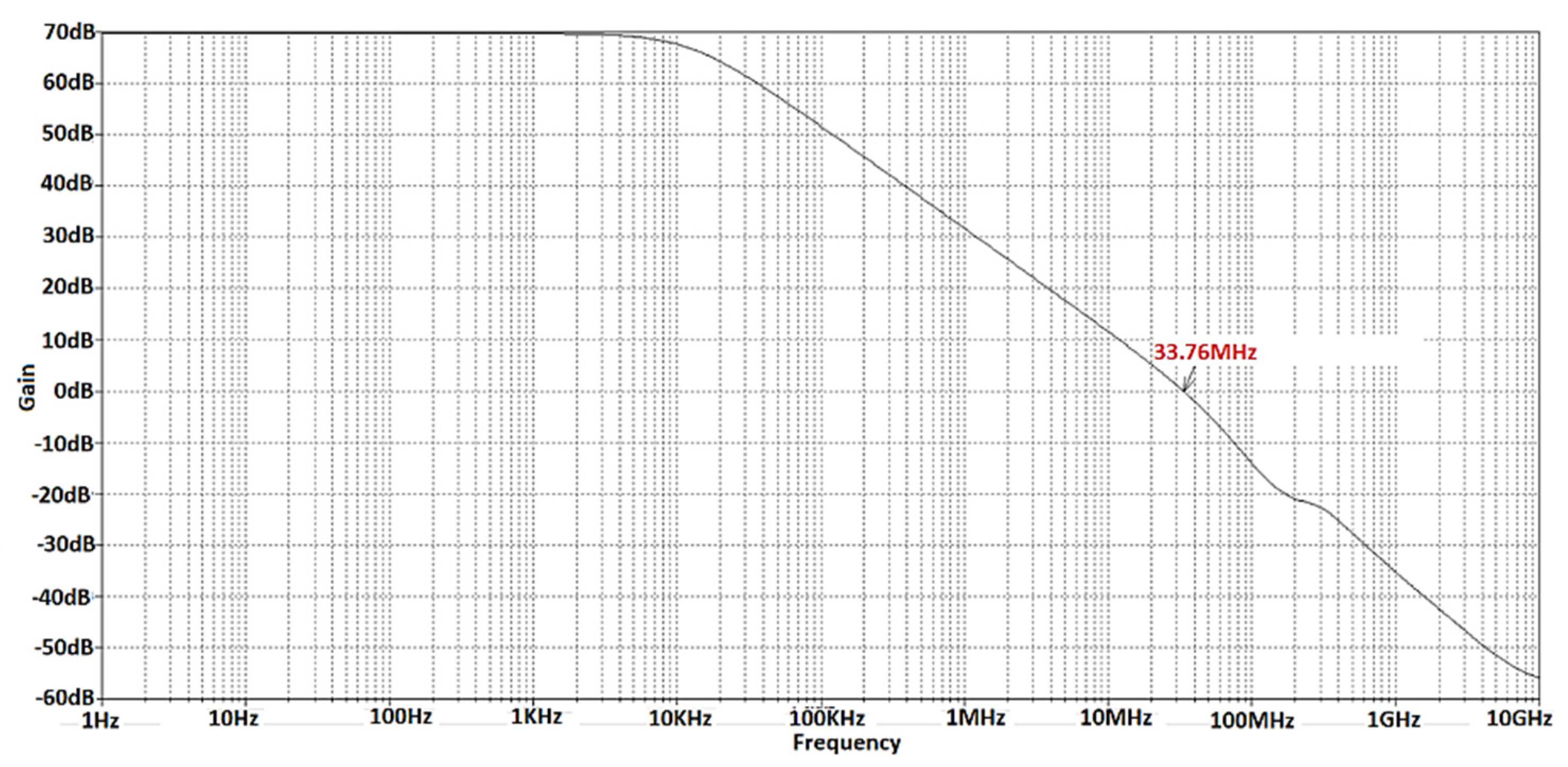
The open loop gain of the proposed operational amplifier circuit is obtained by AC simulation in LTSpice. From Figure 3, the open loop gain of the proposed circuit is 70 dB and the unity gain frequency is approximately 34 MHz.
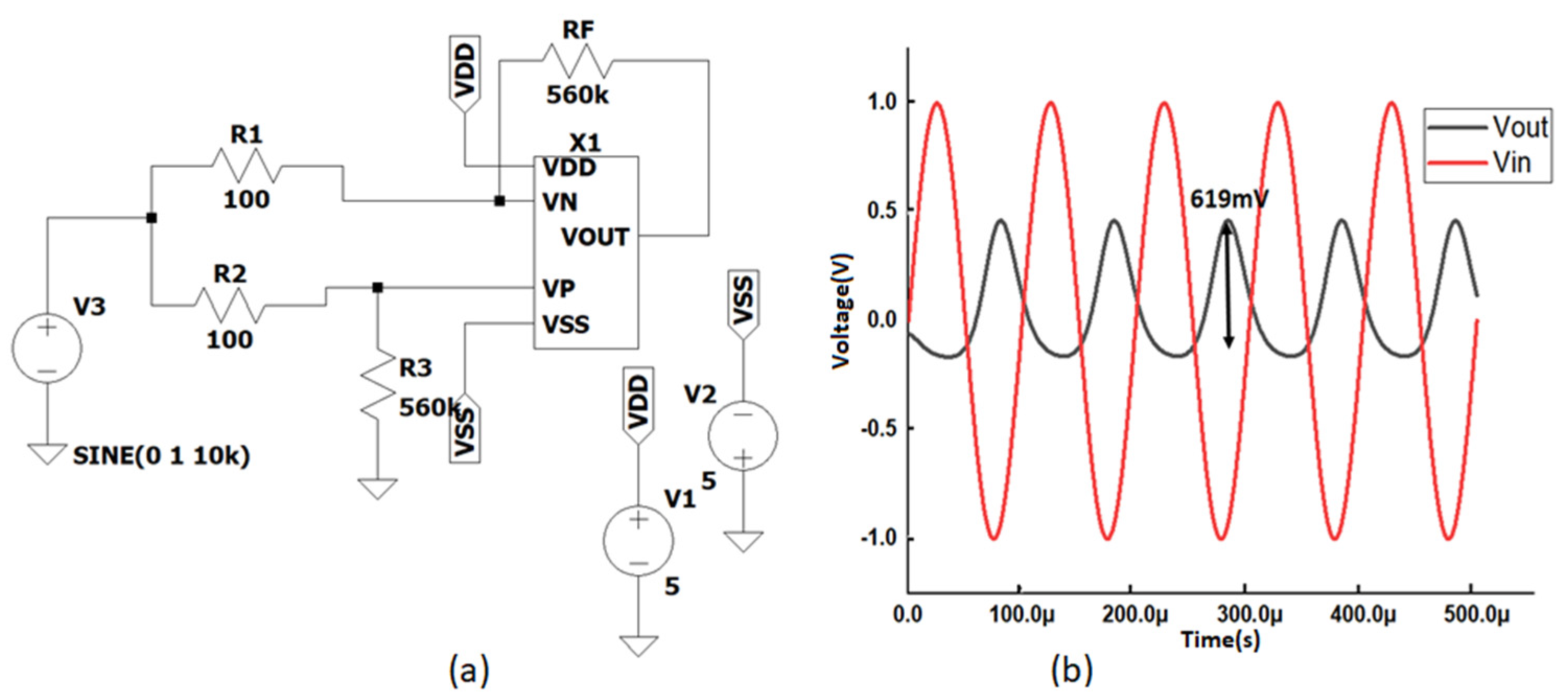
To compute the common mode rejection ratio (CMRR) of the OPA, a simulation setup shown in Figure 4a is designed and a sine wave of 2 V peak-to-peak is applied to the input terminal. Figure 4b shows the simulation result, the output peak-to-peak voltage obtained is 619 mV. CMRR is calculated by using the following equation:
CMRR = ( 1 + R F R 1 ) · ( V i n ( peak to peak ) V o u t ( peak to peak ) )
On putting the values in Equation (8), we obtain:
CMRR = ( 1 + 560 k Ω 100 Ω ) · ( 2 V 619 mV ) = 16158.3
CMRR   in   dB = 20 log ( 16158.3 ) = 84.2 dB  
Slew rate is another important factor of the OPA which can be measured by applying a step signal at the input of OPA and the rate of change of the signal from 10% to 90% at the output of OPA is measured [41]. For computing the slew rate, the proposed OPA is configured in unity gain mode and an ideal pulse of 1 V amplitude is applied to input terminal as shown in Figure 5a. The corresponding simulation output is shown Figure 5b. Slew rate is computed by the following equation:
Slew   rate = Δ V o u t Δ t i m e = ( V o u t 90 % V o u t 10 % ) ( t 90 % t 10 % )
On putting the simulated value from Figure 5b in Equation (10), the slew rate obtained is given as
Slew   rate = ( 898.96 mV 97.92 mV ) ( 1.045 μ s 1.005 μ s ) = 20.03   V μ s

3.1. Operational Amplifier (OPA) as Current to Voltage Converter

To convert the current from PMT into voltage, four transimpedance amplifiers are required as shown in Figure 2. The proposed OPA is configured as transimpedance amplifier as shown in Figure 6a. Resistor R1 is used as feedback resistor and the output voltage of the circuit is given by:
V o u t = I 1 · R 1  
Figure 6b is the simulation result of the transimpedance amplifier, and it shows that, for the applied input current of 1 µA the corresponding output voltage is 1 mV, according to that given by Equation (9). The current from the PSPMT is in the range of tens of µA and Figure 6c shows the linearity of the TIA for the current range from 1 µA to 1 mA.

3.2. OPA as Adder

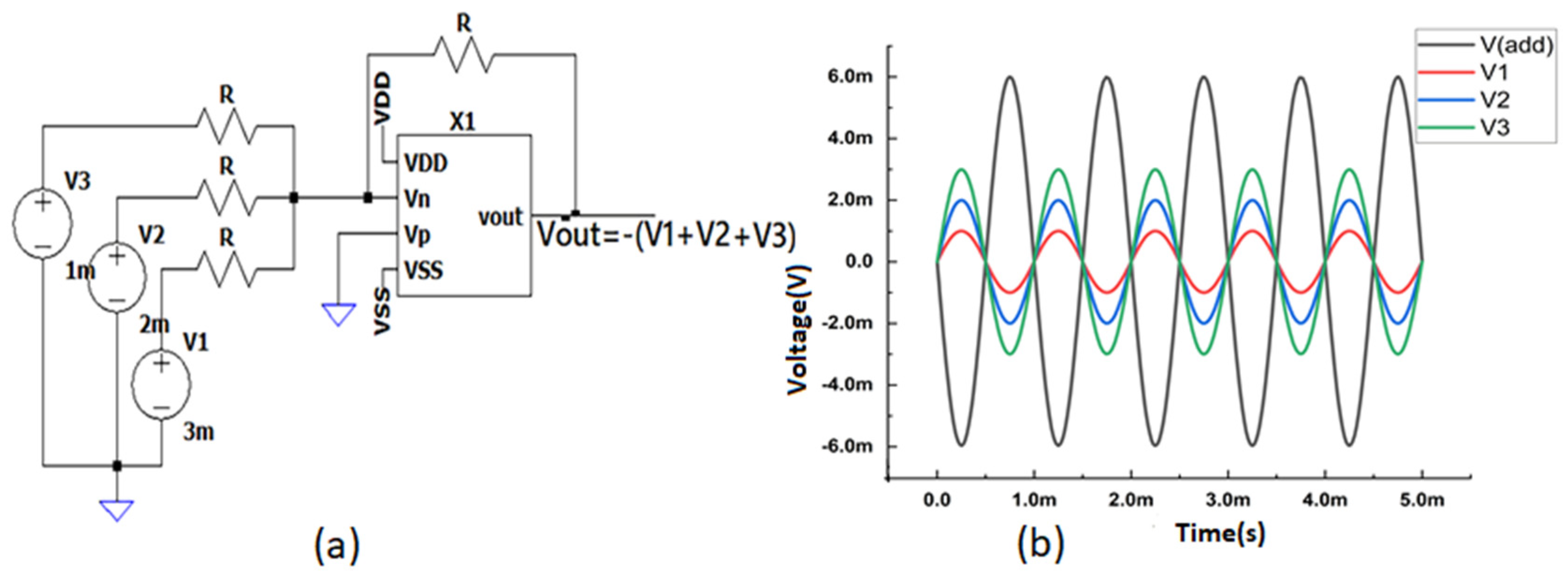
As given in Equations (2)–(4), an adder circuit is required for signal regrouping. The proposed OPA is configured as an adder circuit as shown in Figure 7a. Figure 7b shows the transient simulation result of the circuit. The output voltage of the circuit is the sum of the applied voltages V1, V2, and V3. The gain of the circuit is set to unity by choosing all the resistors of the same value. The amplitude of the applied input voltages is 1 mV, 2 mV, and 3 mV, respectively, and the output voltage is 6 mV as can be seen from Figure 7b.

3.3. OPA as Integrator

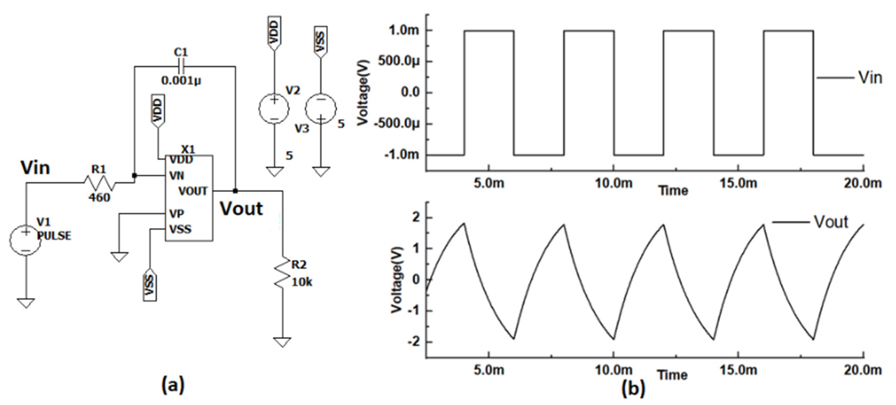
In the readout circuit, integrators are commonly used for pulse shaping or charge-to-time conversion. Our proposed OPA is configured as an integrator as shown in Figure 8a, and the corresponding simulation result is shown in Figure 8b. It can be seen from Figure 8b that the square wave input signal is converted into an approximated ramp signal at the output, verifying the operation of the integrator circuit. A perfect ramp signal cannot be obtained due to the exponential charging and discharging characteristic of capacitor C1.

3.4. Gallium Nitride (GaN) Readout Circuit for Position-Sensitive Photomultiplier Tube (PSPMT)

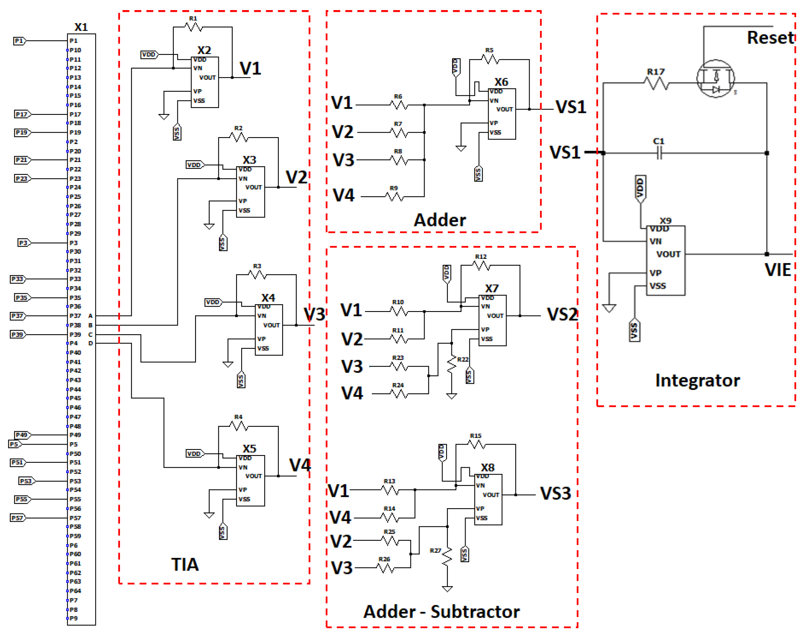
With the various modules designed using our proposed OPA and verified, the complete GaN-based readout circuit is built as shown in Figure 9. Block X1 is discretized position circuit; X2, X3, X4, X5 are the transimpedance amplifiers; X6 is the adder; X7, and X8 are the adder-subtractors. The outputs from the adder and adder-subtractor circuits VS1, VS2, and VS3 will be sent to the data processing unit as shown in Figure 1 for computing the position of the radiation event. The output VS1 is also fed to the input of integrator whose output VIE will be fed to the data processing unit for computing the energy of the radiation event.
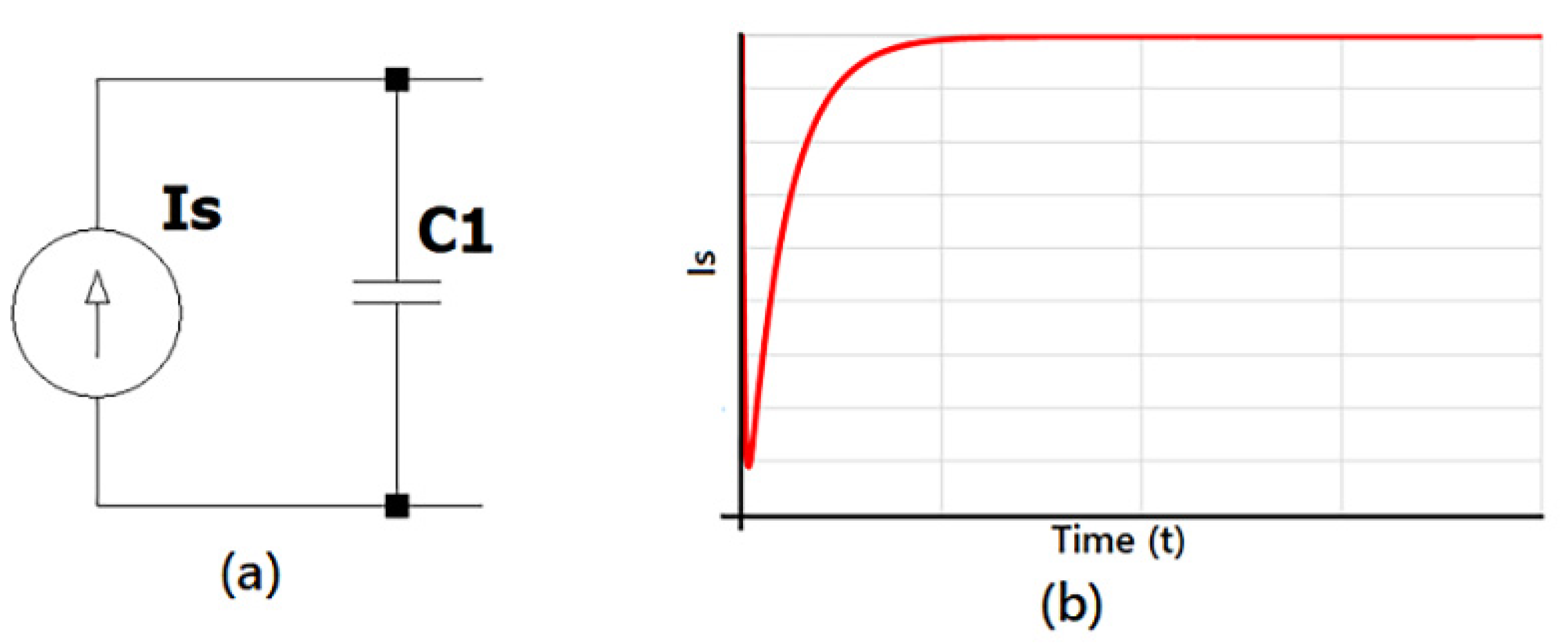
To verify the behavior of the readout circuit, the current obtained from the SiPM due to radiation interaction is mathematically modeled in LTSpice. The PM can be represented by a current source in parallel to a capacitor and the current is given by the Equation (11) [42,43]:
I s = Q e × N P h × P D E × G τ d τ r ( e t τ r e t τ d )  
where Q e is the charge of electron, G is the gain of PMT, PDE is photon detection efficiency of the scintillation crystal, N P h is the number of the photons detected, τ r and τ d are the rise and decay time of the scintillator. The value of the parameters in Equation (13) for S11828-3344M SiPM and CsI(TI) crystal is given in Table 1 [43]. Figure 10 shows the equivalent circuit of PMT and the corresponding current pulse generated by Equation (13), and in our case, the current pulse is 40 μA.
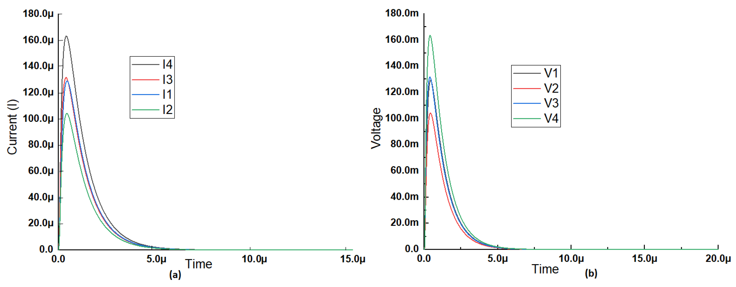
This pulse was applied randomly to different channels of DPC mimicking random radiation events, and the corresponding current signal (I1, I2, I3, I4) obtained from the four channels of the DPC is shown in Figure 11a. These current signals are then converted into voltage signals V1, V2, V3 and V4 by the TIAs shown in Figure 11b. The simulation result shows that the output signal obtained from the TIA has minimal shape distortion and follows Equation (1).
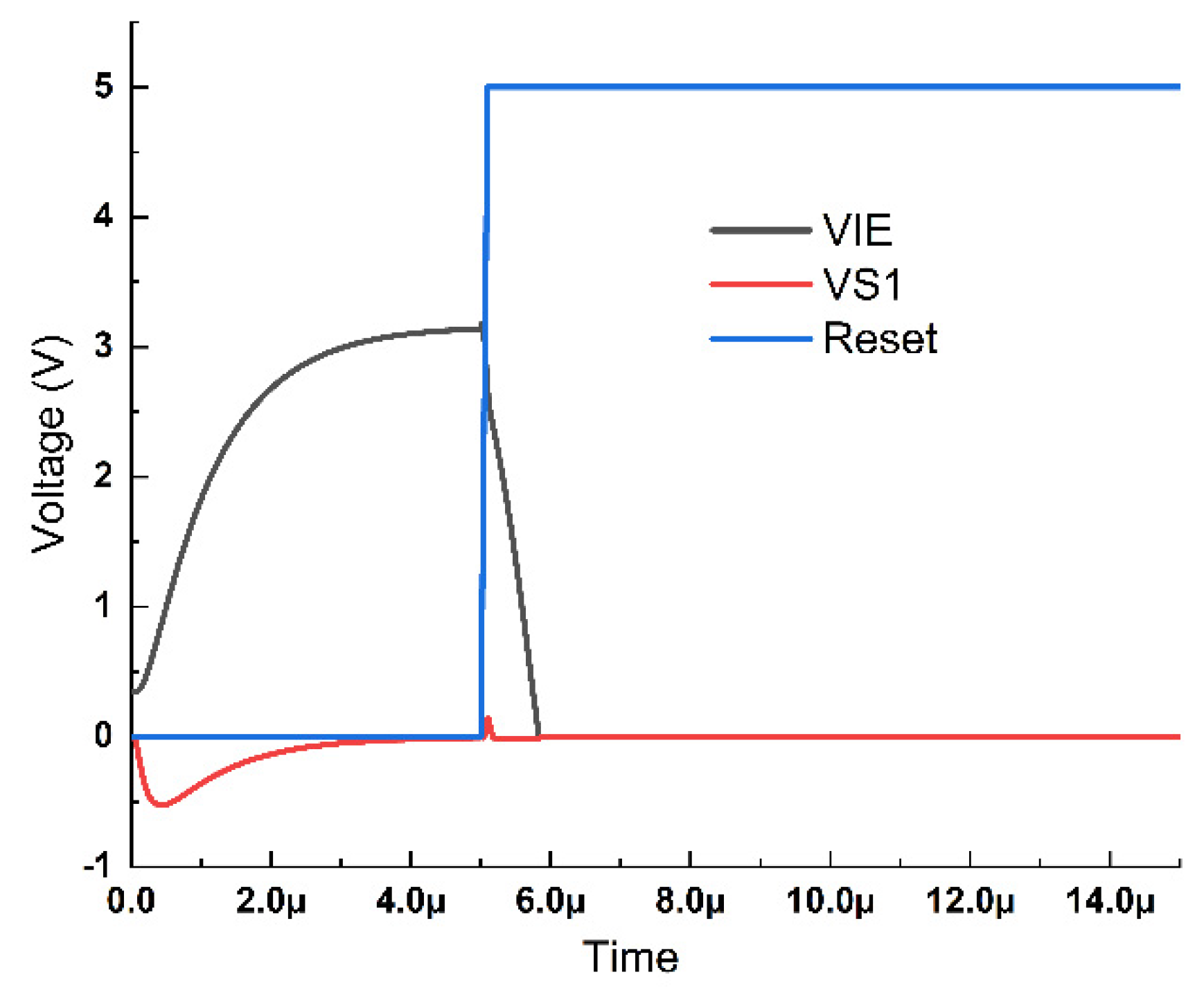
Figure 12 shows the outputs of adder X6, and integrator, respectively. Figure 12 shows that the reset signal remains low until the integration is performed, after that it toggles to the high stage and discharges the capacitor so that the integrator returns to initial state and the next signal will be integrated. The outputs VS1 is the sum of the input currents obtained from DPC as given in Equation (5). Suppose Q1, Q2, Q3 and Q4 are the integral of currents I1, I2, I3 and I4; Q T , which is the sum of Q1 to Q4 representing the total charge collected by the PSPMT and proportional to the energy of the prompt gamma signal.
Thus, VS1 has the information of the energy of the gamma signal. The output VIE of the integrator X9 is given as:
V I E = a V S 1 d t + c
where a and c are constant. The output of the integrator is then feed to the data processing unit for extracting the energy information.
The positioning of the radiation event from the DPC circuit can be determined by the following equations [44,45]:
X = ( A + B ) ( C + D ) A + B + C + D
Y = ( A + D ) ( B + C ) A + B + C + D
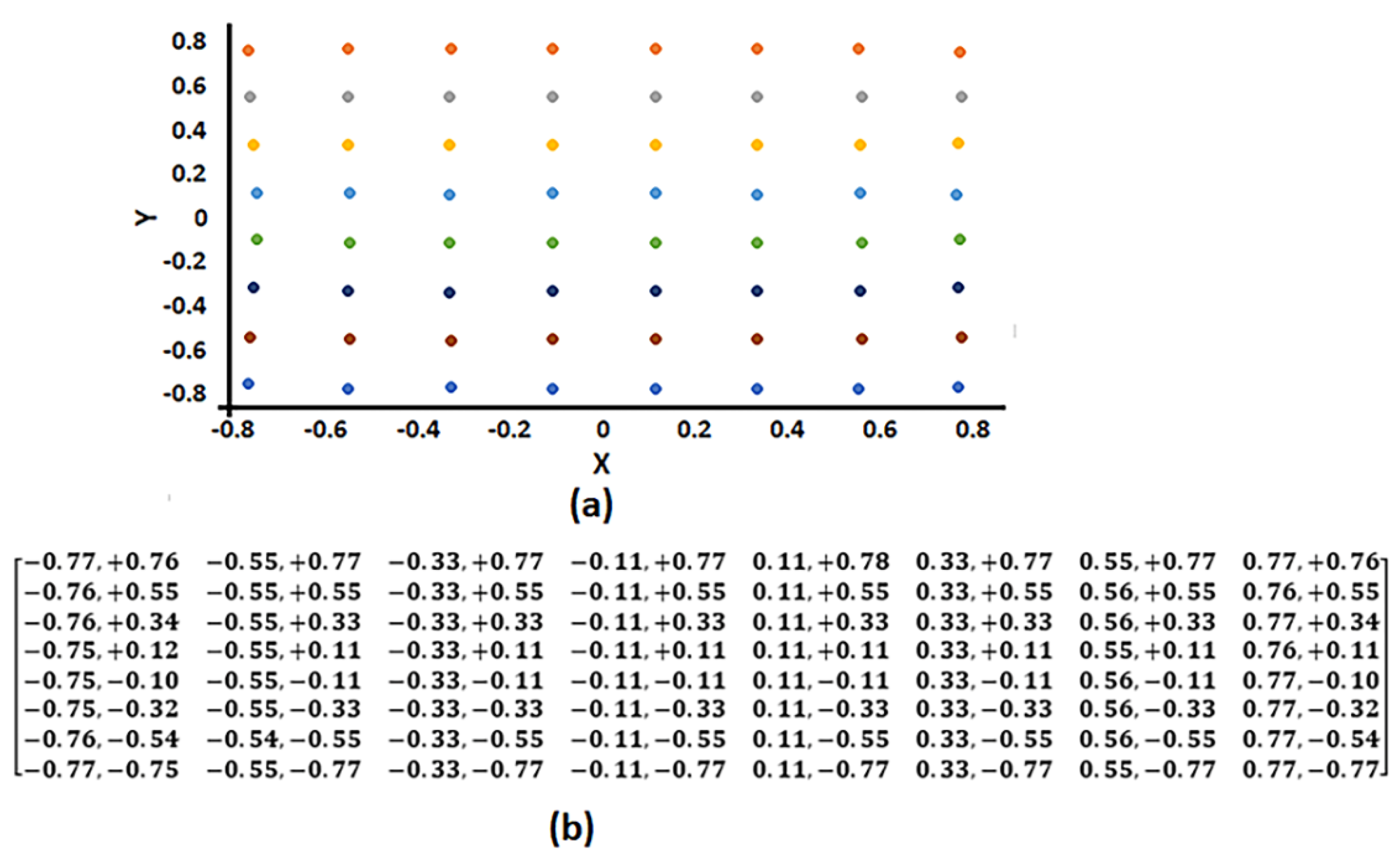
where A, B, C and D represents the peak values of the signals obtained from the four corner channels of the DPC. To verify if the circuit provides the correct position information, the current pulse given by Equation (13) was injected sequentially to each of the input positions of the DPC circuit mimicking the radiation event, and 64 such simulations were independently performed. The detected position information is computed using Equations (15) and (16), where the numerator of Equation (15) is VS2, the denominator of Equation (15) is VS1, the numerator of Equation (16) is VS3, and the denominator of Equation (16) is VS1. Figure 13a shows the detected positions of the PMT arranged in an 8 × 8 array and Figure 13b shows the corresponding position coordinates. The identification of the positions is accurately determined.

4. Conclusions

Prompt gamma imaging is an important technique to locate the Bragg’s peak position and energy. The readout circuits used for prompt gamma detection and processing are in close proximity to the radiation source. Secondary neutrons generated during proton treatment can also negatively affect the performance of the electronic devices present in the treatment room that renders their reliability important. GaN HEMT is more rad-hard compared to the silicon counterpart, and GaN-based operational amplifier is designed in this work.
Simulation results show that the designed OPA has open loop gain of 70 dB and unity gain frequency of 34 MHz. The slew rate of the OPA is 20 V/μs and common mode rejection ratio is 84.2 dB. The proposed OPA is configured for different applications such as transimpedance amplifier, integrator, and the adder which are needed in the prompt gamma readout system. Simulation results show successful operation for these applications. When these different applications are put together, a complete GaN-based prompt gamma readout circuit is implemented, and the result shows successful processing of the prompt gamma signal where its energy and position can be accurately provided for subsequent digital conversion and information extraction.

Author Contributions

Conceptualization, C.T. and V.K.P.; circuit design and simulation, V.K.P.; Writing—original draft preparation, V.K.P.; project administration, C.T.; writing—review and editing, C.T. and V.S.; All authors have read and agreed to the published version of the manuscript.

Funding

This work was funded by Chang Gung University, Grant number CIRPD2F0024.

Conflicts of Interest

All authors have no conflict of interest to the organizations mentioned in the paper.

References

  1. Mukherji, A. Particle Beam Therapy: A Quick View. In Basics of Planning and Management of Patients During Radiation Therapy; Springer: Singapore, 2018. [Google Scholar]
  2. Chuong, M.D.; Mehta, M.P.; Langen, K.; Regine, W.F. The available evidence points to benefits of proton beam therapy. Clin. Adv. Hematol. Oncol. 2014, 12, 861–864. [Google Scholar]
  3. Radhe, M.; David, G. Proton Therapy—Present and Future. Adv. Drug Deliv. 2017, 109, 26–44. [Google Scholar]
  4. Paganetti, H.; Fakhri, G.E.L. Monitoring proton therapy with PET. Br. J. Radiol. 2015, 88, 20150173. [Google Scholar] [CrossRef] [Green Version]
  5. Kurosawa, S.; Kubo, H.; Ueno, K.; Kabuki, S.; Iwaki, S.; Takahashi, M.; Taniue, K.; Higashi, N.; Miuchi, K.; Tanimori, T.; et al. Prompt gamma detection for range verification in proton therapy. Curr. Appl. Phys. 2012, 12, 364–368. [Google Scholar] [CrossRef]
  6. Wronska, A.; Dauvergne, D. Range verification by means of prompt-gamma detection in particle therapy. In Radiation Detection Systems; hal-03085504; CCSD: Charleston, SC, USA, 2020. [Google Scholar]
  7. Aldawood, S.; Thirolf, P.G.; Miani, A.; Böhmer, M.; Dedes, G.; Gernhäuser, R.; Lang, C.; Liprandi, S.; Maier, L.; Marinšek, T.; et al. Development of a Compton camera for prompt-gamma medical imaging. Radiat. Phys. Chem. 2017, 140, 190–197. [Google Scholar] [CrossRef]
  8. Jan, M.L.; Hsiao, I.T.; Huang, H.M. Use of a LYSO-based Compton camera for prompt gamma range verification in proton therapy. Med. Phys. 2017, 44, 6261–6269. [Google Scholar] [CrossRef] [PubMed]
  9. Zhou, W.; Zhang, Z.M.; Li, D.W.; Wang, P.L.; Feng, B.T.; Huang, X.C.; Hu, T.T.; Li, X.H.; Chen, Y.; Wang, Y.J.; et al. A QTC-based signal readout for position-sensitive multi-output detectors. Nucl. Sci. Tech. 2016, 27, 1–7. [Google Scholar] [CrossRef]
  10. Zhang, X.H.; Qi, Y.J.; Zhao, C.L. Design and development of compact readout electronics with silicon photomultiplier array for a compact imaging detector. Chin. Phys. C 2012, 36, 973–978. [Google Scholar] [CrossRef] [Green Version]
  11. Aloufi, K. Neutron Spectroscopy in Proton Therapy; University College of London: London, UK, 2016. [Google Scholar]
  12. Agosteo, S.; Birattari, C.; Caravaggio, M.; Silari, M.; Tosi, G. Secondary neutron and photon dose in proton therapy. Radiother. Oncol. 1998, 48, 293–305. [Google Scholar] [CrossRef]
  13. Wroe, A.J. Evaluation and Mitigation of Secondary Dose Delivered to Electronic Systems in Proton Therapy. Technol. Cancer Res. Treat. 2016, 15, 3–11. [Google Scholar] [CrossRef]
  14. Schneider, U.; Hälg, R. The impact of neutrons in clinical proton therapy. Front. Oncol. 2015, 5, 1–5. [Google Scholar] [CrossRef] [PubMed]
  15. Swami, H.L.; Rathod, R.; Rao, T.S.; Abhangi, M.; Vala, S.; Danani, C.; Chaudhuri, P.; Srinivasan, R. Experimental study of neutron irradiation effect on elementary semiconductor devices using Am-Be neutron source. Indian J. Pure Appl. Phys. 2021, 59, 40–47. [Google Scholar]
  16. Borel, T.; Roig, F.; Michez, A.; Azais, B.; Danzeca, S.; Roche, N.J.H.; Bezerra, F.; Calvel, P.; Dusseau, L. A typical Effect of Displacement Damage on LM124 Bipolar Integrated Circuits. IEEE Trans. Nucl. Sci. 2018, 65, 71–77. [Google Scholar] [CrossRef]
  17. Franco, F.J.; Lozano, J.; Santos, J.P.; Agapito, J.A. Degradation of Instrumentation Amplifiers Due to the Nonionizing Energy Loss Damage. IEEE Trans. Nucl. Sci. 2003, 50, 2433–2440. [Google Scholar] [CrossRef]
  18. Franco, F.J.; Zong, Y.; Casas-Cubillos, J.; Rodríguez-Ruiz, M.A.; Agapito, J.A. Neutron effects on short circuit currents of Op Amps and consequences. IEEE Trans. Nucl. Sci. 2005, 52, 1530–1537. [Google Scholar] [CrossRef] [Green Version]
  19. Yan, L.; Wei, C.; Shanchao, Y.; Xiaoming, J.; Chaohui, H. Synergistic effect of mixed neutron and gamma irradiation in bipolar operational amplifier OP07. Nucl. Instruments Methods Phys. Res. Sect. A Accel. Spectrometers Detect. Assoc. Equip. 2016, 831, 334–338. [Google Scholar] [CrossRef]
  20. Assaf, J. Radiation and annealing effects on integrated bipolar Operational Amplifier. Radiat. Phys. Chem. 2017, 131, 100–104. [Google Scholar] [CrossRef]
  21. Boley, W.R. Compendia of TID and neutron radiation test results of selected COTS parts. In Proceedings of the 2008 IEEE Radiation Effects Data Workshop, Tucson, AZ, USA, 14–18 July 2008; pp. 142–147. [Google Scholar]
  22. Amir, H.F.A.; Chee, F.P.; Salleh, S. Effects of high energy neutrons and resulting secondary charged particles on the operation of MOSFETs. In Proceedings of the 2014 International Conference on Computational Science and Technology, ICCST, Kota Kinabalu, Malaysia, 27–28 August 2014. [Google Scholar]
  23. Chao, D.S.; Shih, H.Y.; Jiang, J.Y.; Huang, C.F.; Chiang, C.Y.; Ku, C.S.; Yen, C.T.; Lee, L.S.; Hsu, F.J.; Chu, K.T.; et al. Influence of displacement damage induced by neutron irradiation on effective carrier density in 4H-SiC SBDs and MOSFETs. Jpn. J. Appl. Phys. 2019, 58, SBBD08. [Google Scholar] [CrossRef]
  24. Abdul Amir, H.F.; Chik, A. Neutron radiation effects on metal oxide semiconductor (MOS) devices. Nucl. Instrum. Methods Phys. Res. Sect. B Beam Interact. Mater. Atoms 2009, 267, 3032–3036. [Google Scholar] [CrossRef]
  25. Makowski, D. The Impact of Radiation on Electronic Devices with Special Consideration of Neutron and Gamma Radiation Monitoring; Technical University of Lodz: Lodz, Poland, 2006. [Google Scholar]
  26. Haider, F.A.; Chee, F.P.; Abu Hassan, H.; Saafie, S.; Afishah, A. Changes in electrical properties of MOS transistor induced by single 14 MeV neutron. In Proceedings of the AIP Conference Proceedings, Online, 22 January 2016; Volume 1704, p. 050015. [Google Scholar]
  27. Vaidya, S.J.; Sharma, D.K.; Chandorkar, A.N. Neutron induced oxide degradation in MOSFET structures. In Proceedings of the International Symposium on the Physical and Failure Analysis of Integrated Circuits, IPFA 2003, Singapore, 11 July 2003; pp. 151–155. [Google Scholar]
  28. Angela Chen Gallium Nitride is the Silicon of the Future. Available online: https://www.theverge.com/2018/11/1/18051974/gallium-nitride-anker-material-silicon-semiconductor-energy#:~:text=GaN has a wider band,on GaN in power electronics (accessed on 11 April 2021).
  29. Where is GaN Going? Available online: https://epc-co.com/epc/GalliumNitride/whereisgangoing.aspx (accessed on 12 April 2021).
  30. Scharf, A. Gallium Nitride is Moving Forward; Power Electronics Europe: Munich, Germany, 2016. [Google Scholar]
  31. Zafrani, M. Radiation Performance of Enhancement-Mode Gallium Nitride Power Devices; EE Power: Hatfield, UK, 2020; pp. 40–42. [Google Scholar]
  32. Hazdra, P.; Popelka, S. Radiation resistance of wide-bandgap semiconductor power transistors. Phys. Status Solidi Appl. Mater. Sci. 2017, 214, 1–8. [Google Scholar] [CrossRef]
  33. Cha, S.; Chung, Y.H.; Wojtowwicz, M.; Smorchkova, I.; Allen, B.R.; Yang, J.M.; Kagiwada, R. Wideband AlGaN/GaN HEMT low noise amplifier for highly survivable receiver electronics. In Proceedings of the IEEE MTT-S International Microwave Symposium Digest, Fort Worth, TX, USA, 6–11 June 2004; pp. 829–831. [Google Scholar]
  34. Pengelly, R.; Sheppard, S.; Smith, T.; Pribble, B.; Wood, S.; Platis, C. Commercial Gan devices for switching and low noise applications. In Proceedings of the 2011 International Conference on Compound Semiconductor Manufacturing Technology, CS MANTECH 2011, Palm Springs, CA, USA, 16–19 May 2011; pp. 27–30. [Google Scholar]
  35. Helali, A.; Gassoumi, M.; Gassoumi, M.; Maaref, H. Design and Optimization of LNA Amplifier Based on HEMT GaN for X-Band Wireless-Communication and IoT Applications. Silicon 2020, 1–9. [Google Scholar] [CrossRef]
  36. Pandey, V.K.; Tan, C.M. Application of Gallium Nitride Technology in Particle Therapy Imaging. IEEE Trans. Nucl. Sci. 2021, 68, 1319–1324. [Google Scholar] [CrossRef]
  37. Zafrani, M.; Lidow, A. Radiation Performance of Enhancement-Mode Gallium Nitride Power Devices. Available online: https://epc-co.com/epc/EventsandNews/News/ArtMID/1627/ArticleID/2933/Radiation-Performance-of-Enhancement-Mode-Gallium-Nitride-Power-Devices.aspx (accessed on 26 April 2021).
  38. Lidow, A.; Smalley, K. Radiation Tolerant Enhancement Mode Gallium Nitride ( eGaN ®) FET Characteristics. In Proceedings of the GOMAC Tech Conference, Las Vegas, NV, USA, 19–22 March 2012. [Google Scholar]
  39. Lidow, A.; Nakata, A.; Rearwin, M.; Strydom, J.; Zafrani, A.M. Single-event and radiation effect on enhancement mode gallium nitride FETs. In Proceedings of the IEEE Radiation Effects Data Workshop, Paris, France, 14–18 July 2014; pp. 1–7. [Google Scholar]
  40. Siegel, S.; Silverman, R.W.; Shao, Y.; Cherry, S.R. Simple charge division readouts for imaging scintillator arrays using a multi-channel PMT. IEEE Trans. Nucl. Sci. 1996, 43, 1634–1641. [Google Scholar] [CrossRef]
  41. Slew Rate. Available online: https://training.ti.com/system/files/docs/1221-Slew Rate 1-slides.pdf (accessed on 22 March 2021).
  42. Seifert, S.; Van Dam, H.T.; Huizenga, J.; Vinke, R.; Dendooven, P.; Löhner, H.; Schaart, D.R. Simulation of silicon photomultiplier signals. IEEE Trans. Nucl. Sci. 2009, 56, 3726–3733. [Google Scholar] [CrossRef]
  43. Massari, R.; Soluri, A.; Caputo, D.; Ronchi, S. Low power readout circuits for large area silicon photomultiplier array. In Proceedings of the 6th International Workshop on Advances in Sensors and Interfaces (IWASI), Gallipoli, Italy, 18–19 June 2015; pp. 158–162. [Google Scholar]
  44. Olcott, P.D.; Talcott, J.A.; Levin, C.S.; Habte, F.; Foudray, A.M.K. Compact readout electronics for Position Sensitive Photomultiplier Tubes. In Proceedings of the IEEE Nuclear Science Symposium Conference Record; IEEE: Piscataway, NJ, USA, 2003; Volume 3, pp. 1962–1966. [Google Scholar]
  45. Jeon, S.J.; Kim, J.; Ji, M.G.; Park, J.H.; Choi, Y.W. Position Error Correction Using Homography in Discretized Positioning Circuit for Gamma-Ray Imaging Detection System. IEEE Trans. Nucl. Sci. 2017, 64, 816–819. [Google Scholar] [CrossRef]
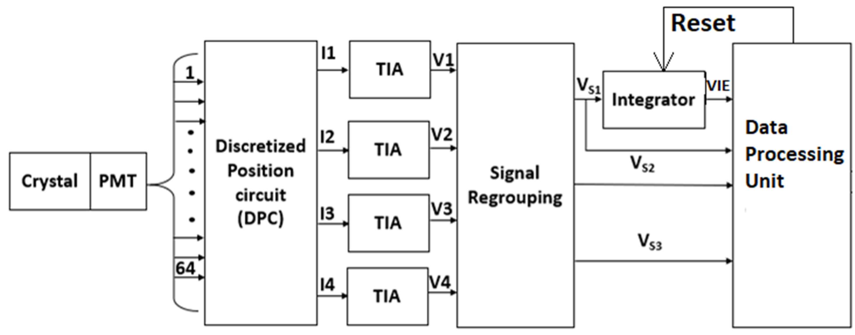
Figure 1. Signal readout block diagram.
Applsci 11 05606 g001
Figure 2. Proposed gallium nitride (GaN) operational amplifier. Exact values of the components cannot be shown here due to confidentiality pertaining to patent filing.
Applsci 11 05606 g002
Figure 3. Open loop gain of proposed operational amplifier having a unity gain frequency of 33.76 MHz.
Applsci 11 05606 g003
Figure 4. (a) Common mode rejection ratio (CMRR) simulation setup. (b) Simulation output.
Applsci 11 05606 g004
Figure 5. (a) Slew rate simulation model. (b) Simulation output.
Applsci 11 05606 g005
Figure 6. (a) Operational amplifier (OPA) as transimpedance amplifier (b) Simulation result (c) Simulation results showing the Linearity of TIA for 1 µA to 1 mA input current.
Applsci 11 05606 g006aApplsci 11 05606 g006b
Figure 7. (a) Adder circuit. (b) Simulation output.
Applsci 11 05606 g007
Figure 8. (a) Integrator circuit. (b) Simulation output.
Applsci 11 05606 g008
Figure 9. Simulation model of the GaN readout system.
Applsci 11 05606 g009
Figure 10. (a) Equivalent circuit of SiPM. (b) Current pulse generated from scintillation.
Applsci 11 05606 g010
Figure 11. (a) Output current from four channels of discretized position circuit (DPC). (b) Output voltage of transimpedance amplifiers (TIAs).
Applsci 11 05606 g011
Figure 12. Simulation output of adder and integrator.
Applsci 11 05606 g012
Figure 13. Position verification of the readout circuit. (a) position of the input current pulse applied mutual exclusively. (b) Computed position coordinates that correspond to the individual input current pulse.
Applsci 11 05606 g013
Table 1. Silicon photomultiplier (SiPM) current pulse parameters.
ParameterValue
N P h 1000
G7.5 × 105
PDE0.40
τ d ( n s ) 50
τ r ( μ s ) 1
Publisher’s Note: MDPI stays neutral with regard to jurisdictional claims in published maps and institutional affiliations.