Structural Modifications in Epitaxial Graphene on SiC Following 10 keV Nitrogen Ion Implantation

 ,
,
Abstract
1. Introduction
2. Materials and Methods
3. Results
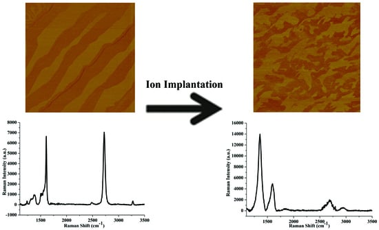
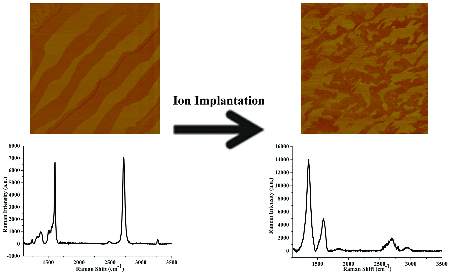
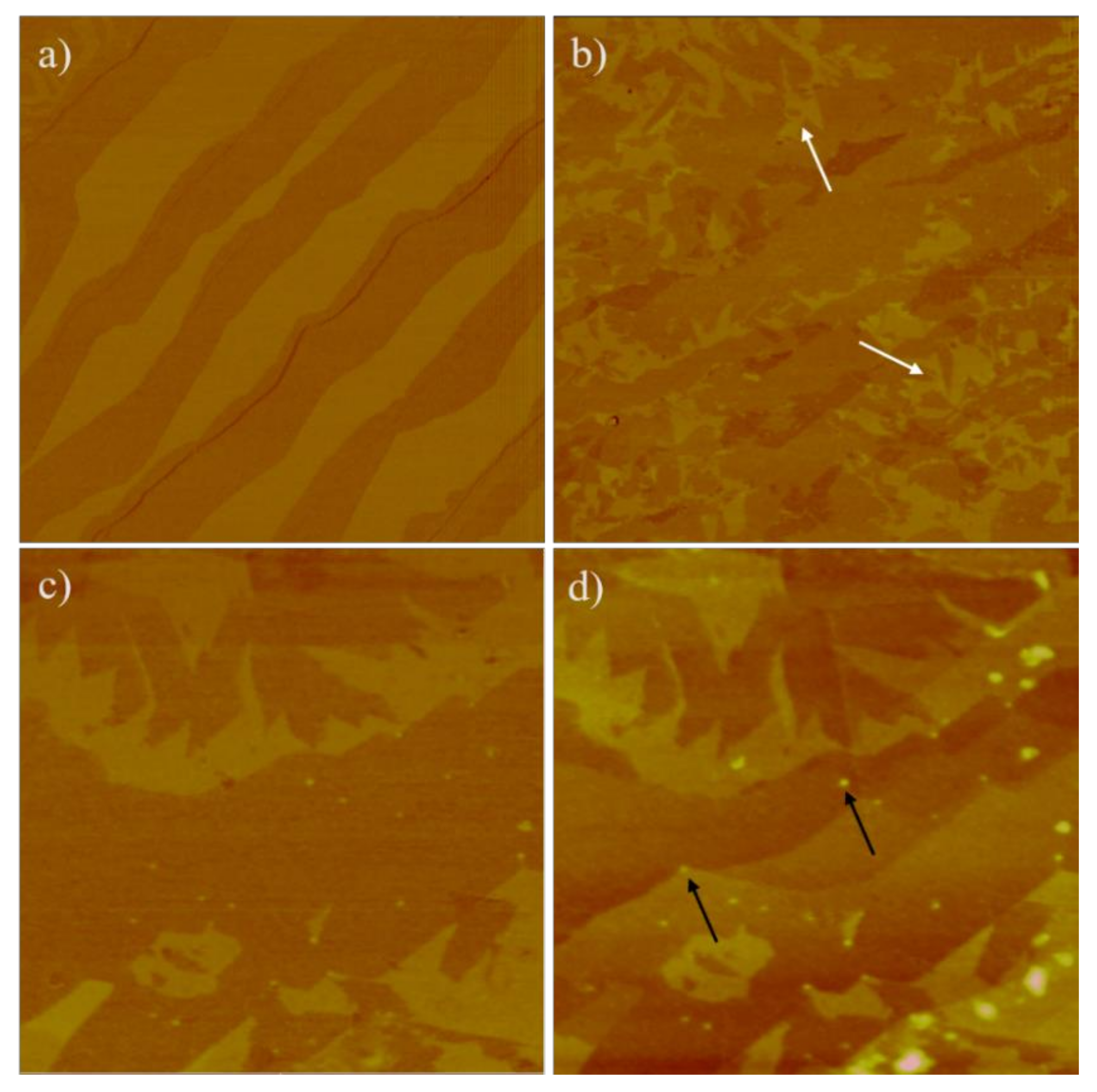
3.1. AFM
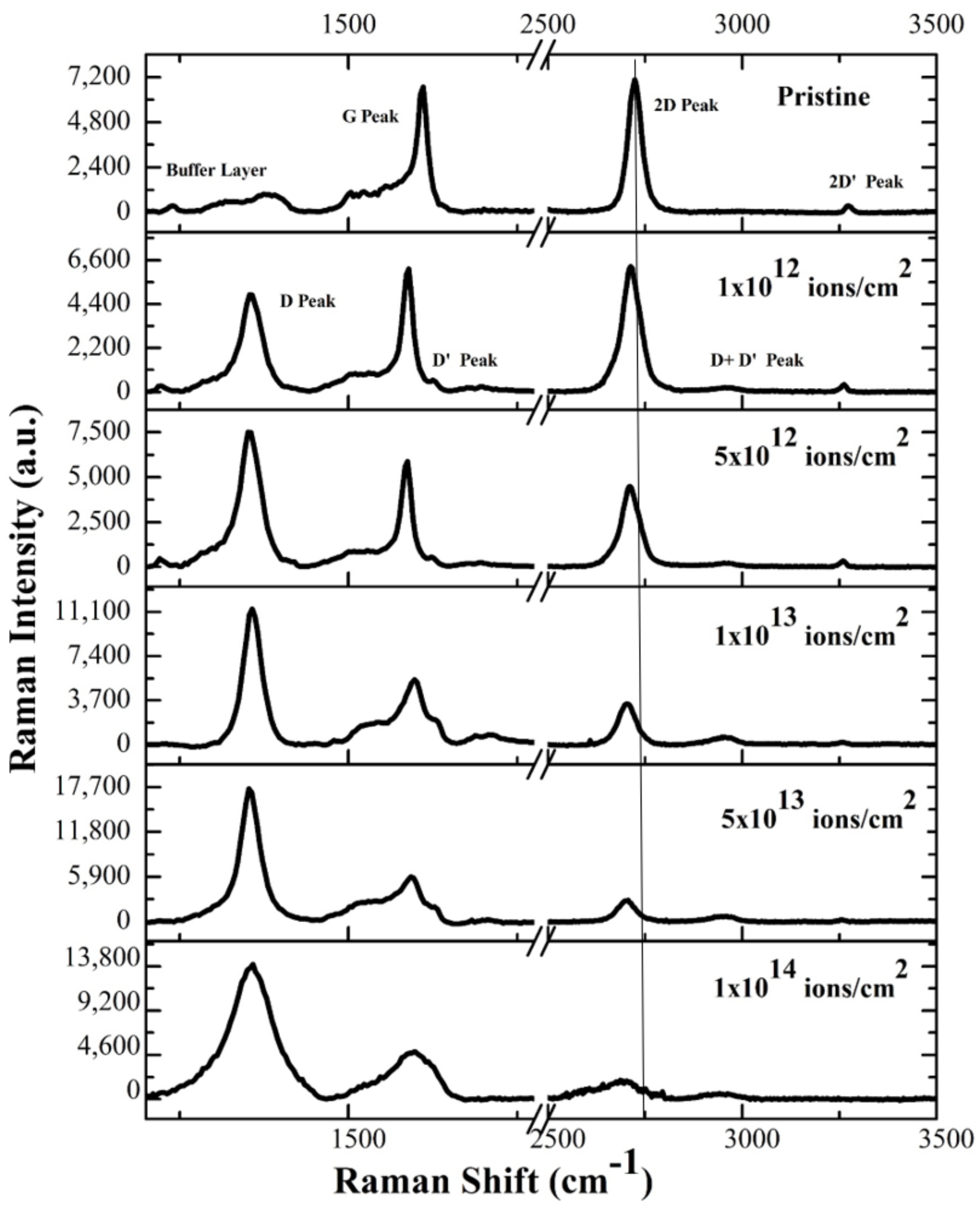
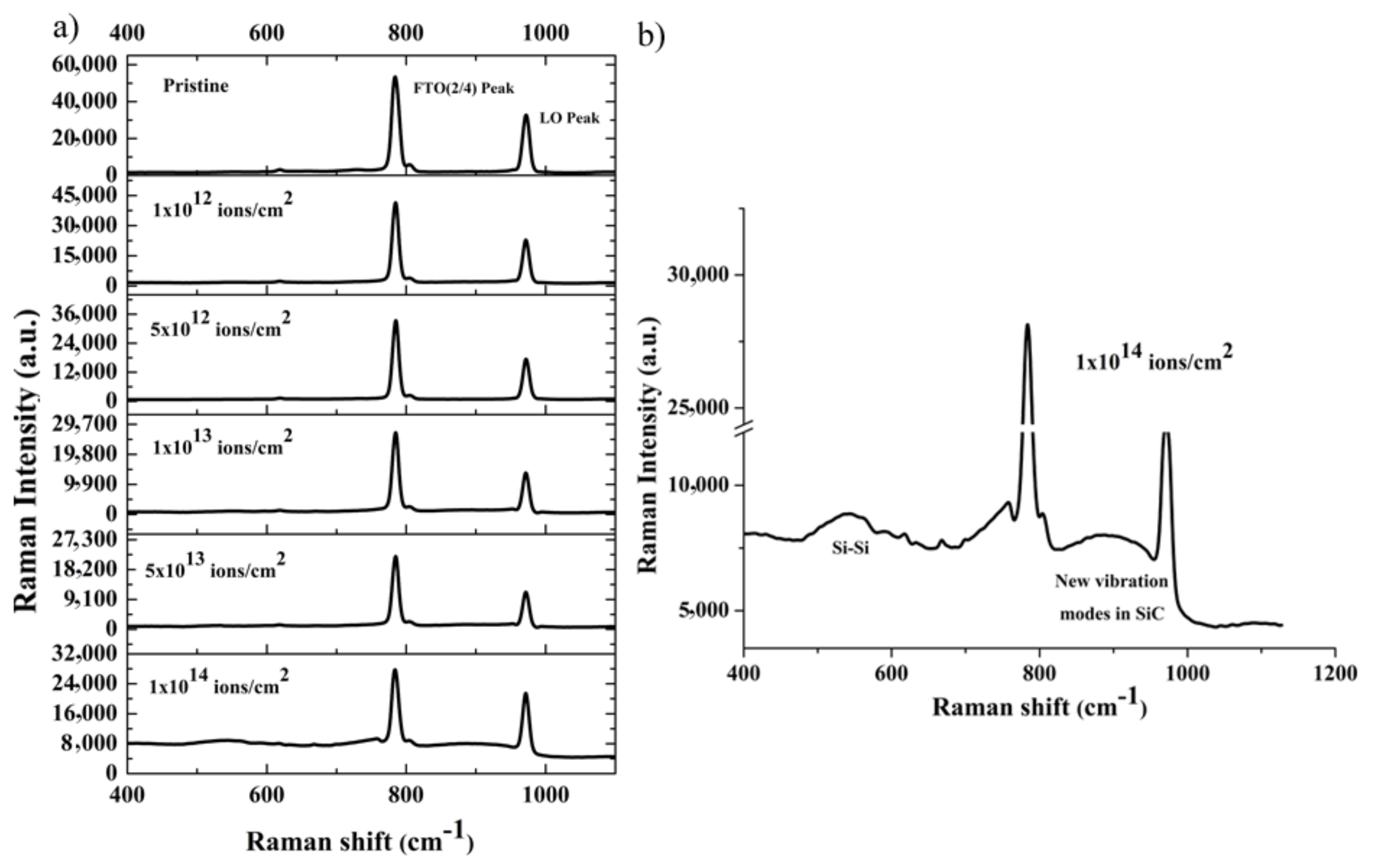
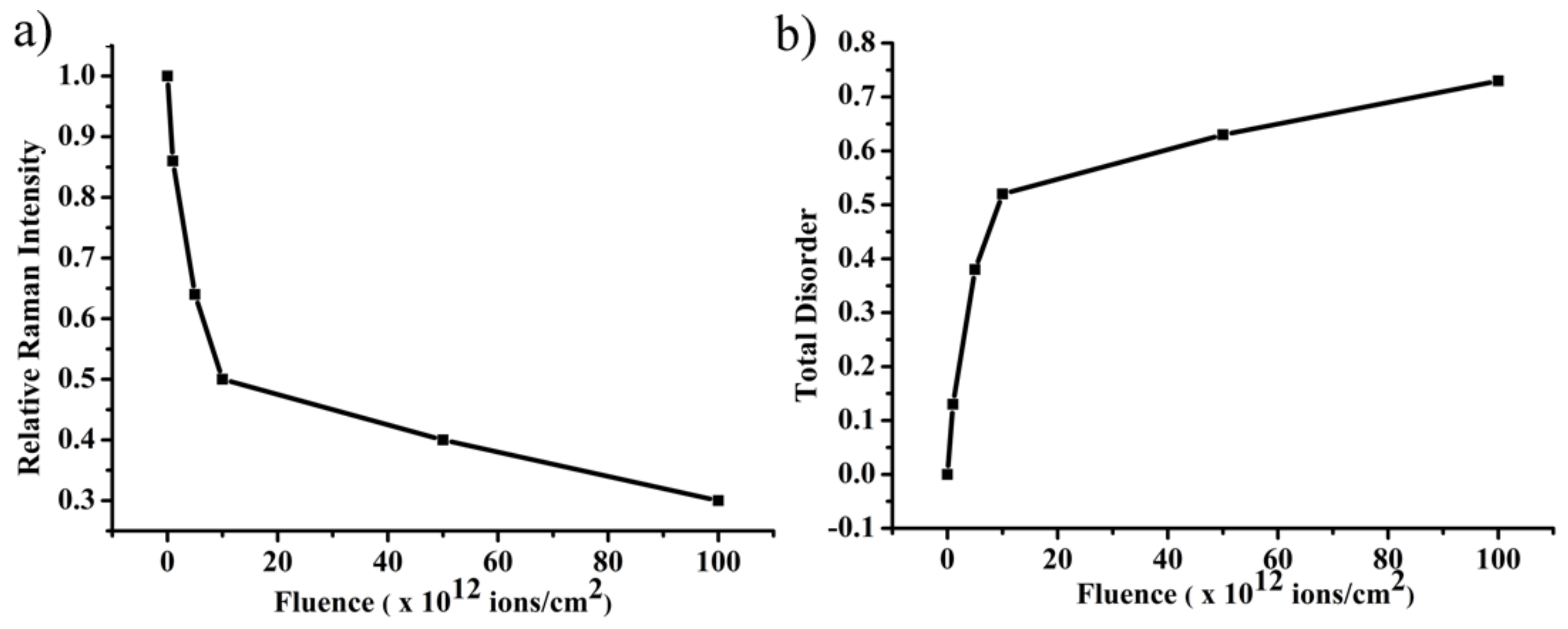
3.2. Raman Spectroscopy
3.3. XPS
4. Conclusions
Author Contributions
Funding
Conflicts of Interest
References
- Geim, A.K.; Novoselov, K.S. The rise of graphene. Nat. Mater. 2007, 6, 183–191. [Google Scholar] [CrossRef] [PubMed]
- Dvorak, M.; Oswald, W.; Wu, Z. Bandgap Opening by Patterning Graphene. Sci. Rep. 2013, 3. [Google Scholar] [CrossRef] [PubMed]
- Dabrowski, P.; Rogala, M.; Wlasny, I.; Klusek, Z.; Kopciuszyński, M.; Jalochowski, M.; Strupiński, W.; Baranowski, J. Nitrogen doped epitaxial graphene on 4H-SiC(0001)—Experimental and theoretical study. Carbon 2015, 94, 214–223. [Google Scholar] [CrossRef]
- Thiele, C.; Felten, A.; Echtermeyer, T.; Ferrari, A.C.; Casiraghi, C.; Löhneysen, H.V.; Krupke, R. Electron-beam-induced direct etching of graphene. Carbon 2013, 64, 84–91. [Google Scholar] [CrossRef]
- Daukiya, L.; Mattioli, C.; Aubel, D.; Hajjar-Garreau, S.; Vonau, F.; Denys, E.; Reiter, G.; Fransson, J.; Perrin, E.; Bocquet, M.-L.; et al. Covalent Functionalization by Cycloaddition Reactions of Pristine Defect-Free Graphene. ACS Nano 2017, 11, 627–634. [Google Scholar] [CrossRef] [PubMed]
- Wu, X.; Zhao, H.; Yan, D.; Pei, J. Investigation on gallium ions impacting monolayer graphene. AIP Adv. 2015, 5, 067171. [Google Scholar] [CrossRef]
- Wang, Q.; Shao, Y.; Ge, D.; Yang, Q.; Ren, N. Surface modification of multilayer graphene using Ga ion irradiation. J. Appl. Phys. 2015, 117, 165303. [Google Scholar] [CrossRef]
- Wang, Q.; Dong, J.; Bai, B.; Xie, G. Investigating change of properties in gallium ion irradiation patterned single-layer graphene. Phys. Lett. A 2016, 380, 3514–3519. [Google Scholar] [CrossRef]
- Kwon, K.C.; Son, P.K.; Kim, S.Y. Ion beam irradiation of few-layer graphene and its application to liquid crystal cells. Carbon 2014, 67, 352–359. [Google Scholar] [CrossRef]
- Xie, G.; Yang, R.; Chen, P.; Zhang, J.; Tian, X.; Wu, S.; Zhao, J.; Cheng, M.; Yang, W.; Wang, D.; et al. A General Route Towards Defect and Pore Engineering in Graphene. Small 2014, 10, 2280–2284. [Google Scholar] [CrossRef] [PubMed]
- Naitou, Y.; Iijima, T.; Ogawa, S. Direct nano-patterning of graphene with helium ion beams. Appl. Phys. Lett. 2015, 106, 033103. [Google Scholar] [CrossRef]
- Morin, A.; Lucot, D.; Ouerghi, A.; Patriarche, G.; Bourhis, E.; Madouri, A.; Ulysse, C.; Pelta, J.; Auvray, L.; Jede, R.; et al. FIB carving of nanopores into suspended graphene films. Microelectron. Eng. 2012, 97, 311–316. [Google Scholar] [CrossRef]
- Xu, Y.; Zhang, K.; Brusewitz, C.; Wu, X.; Hofsass, H.C. Investigation of the effect of low energy ion beam irradiation on mono-layer graphene. AIP Adv. 2013, 3, 72120. [Google Scholar] [CrossRef]
- Willke, P.; Amani, J.A.; Thakur, S.; Weikert, S.; Druga, T.; Maiti, K.; Hofsäss, H.; Wenderoth, M. Short-range ordering of ion-implanted nitrogen atoms in SiC-graphene. Appl. Phys. Lett. 2014, 105, 111605. [Google Scholar] [CrossRef]
- Willke, P.; Amani, J.A.; Sinterhauf, A.; Thakur, S.; Kotzott, T.; Druga, T.; Weikert, S.; Maiti, K.; Hofsäss, H.; Wenderoth, M. Doping of Graphene by Low-Energy Ion Beam Implantation: Structural, Electronic, and Transport Properties. Nano Lett. 2015, 15, 5110–5115. [Google Scholar] [CrossRef] [PubMed]
- Zhao, J.-H.; Qin, X.-F.; Wang, F.-X.; Fu, G.; Wang, X.-L. Raman and morphology visualization in epitaxial graphene on 4H-SiC by Nitrogen or Argon ion irradiation. Nucl. Instrum. Methods Phys. Res. Sect. B Beam Int. Mater. Atoms 2015, 365, 260–263. [Google Scholar] [CrossRef]
- Kaushik, P.D.; Rodner, M.; Lakshmi, G.B.V.S.; Ivanov, I.G.; Greczynski, G.; Palisaitis, J.; Eriksson, J.; Solanki, P.R.; Aziz, A.; Siddiqui, A.M.; et al. Surface functionalization of epitaxial graphene using ion implantation for sensing and optical applications. Carbon 2020, 157, 169–184. [Google Scholar] [CrossRef]
- Kaushik, P.D.; Ivanov, I.G.; Lin, P.-C.; Kaur, G.; Eriksson, J.; Lakshmi, G.; Avasthi, D.; Gupta, V.; Aziz, A.; Siddiqui, A.M.; et al. Surface functionalization of epitaxial graphene on SiC by ion irradiation for gas sensing application. Appl. Surf. Sci. 2017, 403, 707–716. [Google Scholar] [CrossRef]
- Compagnini, G.; Giannazzo, F.; Sonde, S.; Raineri, V.; Rimini, E. Ion irradiation and defect formation in single layer graphene. Carbon 2009, 47, 3201–3207. [Google Scholar] [CrossRef]
- Ochedowski, O.; Bussmann, B.K.; D’Etat, B.B.; Lebius, H.; Schleberger, M. Manipulation of the graphene surface potential by ion irradiation. Appl. Phys. Lett. 2013, 102, 153103. [Google Scholar] [CrossRef]
- Sorieul, S.; Costantini, J.-M.; Gosmain, L.; Calas, G.; Grob, J.-J.; Thomé, L. Study of damage in ion-irradiated α-SiC by optical spectroscopy. J. Phys. Condens. Matter 2006, 18, 8493–8502. [Google Scholar] [CrossRef] [PubMed]
- Kaushik, P.D.; Aziz, A.; Siddiqui, A.M.; Lakshmi, G.; Syväjärvi, M.; Yakimova, R.; Yazdi, G.R. Structural and optical modification in 4H-SiC following 30 keV silver ion irradiation. (International Conference on Inventive Research in Material Science and Technology, Hotel Arcadia, Coimbatore, Tamil Nadu, India, 23–24 March 2018). AIP Conf. Proc. 2018, 1966, 020035. [Google Scholar] [CrossRef]
- Granzier-Nakajima, T.; Fujisawa, K.; Anil, V.; Terrones, M.; Yeh, Y.-T. Controlling Nitrogen Doping in Graphene with Atomic Precision: Synthesis and Characterization. Nanomater 2019, 9, 425. [Google Scholar] [CrossRef] [PubMed]
- Lee, W.J.; Lim, J.; Kim, S.O. Carbon Nanomaterials: Nitrogen Dopants in Carbon Nanomaterials: Defects or a New Opportunity? (Small Methods 1-2/2017). Small Methods 2017, 1. [Google Scholar] [CrossRef]
- Yazdi, G.; Vasiliauskas, R.; Iakimov, T.; Zakharov, A.; Syväjärvi, M.; Yakimova, R. Growth of large area monolayer graphene on 3C-SiC and a comparison with other SiC polytypes. Carbon 2013, 57, 477–484. [Google Scholar] [CrossRef]
- Ziegler, J.F.; Ziegler, M.D.; Biersack, J.P. SRIM—The stopping and range of ions in matter. Nucl. Instrum. Methods Phys. Res. Sect. B Beam Interact. Mater. At. 2010, 268, 1818–1823. [Google Scholar] [CrossRef]
- Walton, J.; Wincott, P.; Fairley, N.; Carrick, A. Peak Fitting with CasaXPS: A Casa Pocket Book; Accolyte Science: Knutsford, UK, 2010. [Google Scholar]
- Lehtinen, O.; Kotakoski, J.; Krasheninnikov, A.V.; Tolvanen, A.; Nordlund, K.; Keinonen, J. Effects of ion bombardment on a two-dimensional target: Atomistic simulations of graphene irradiation. Phys. Rev. B 2010, 81, 153401. [Google Scholar] [CrossRef]
- Devanathan, R.; Weber, W.J.; Gao, F. Atomic scale simulation of defect production in irradiated 3C-SiC. J. Appl. Phys. 2001, 90, 2303–2309. [Google Scholar] [CrossRef]
- Chang, J.; Cho, J.-Y.; Gil, C.-S.; Lee, W.-J. A Simple method to calculate the displacement damage cross section of silicon carbide. Nucl. Eng. Technol. 2014, 46, 475–480. [Google Scholar] [CrossRef]
- Saito, Y.; Yoshikawa, T.; Inagaki, M.; Tomita, M.; Hayashi, T. Growth and structure of graphitic tubules and polyhedral particles in arc-discharge. Chem. Phys. Lett. 1993, 204, 277–282. [Google Scholar] [CrossRef]
- Dutta, N.; Mohanty, S.; Buzarbaruah, N. Modification on graphite due to helium ion irradiation. Phys. Lett. A 2016, 380, 2525–2530. [Google Scholar] [CrossRef]
- Malard, L.M.; Pimenta, M.A.; Dresselhaus, G.; Dresselhaus, M.S. Raman spectroscopy in graphene. Phys. Rep. 2009, 473, 51–87. [Google Scholar] [CrossRef]
- Beams, R.; Cançado, L.G.; Novotny, L. Raman characterization of defects and dopants in graphene. J. Phys. Condens. Matter 2015, 27, 83002. [Google Scholar] [CrossRef] [PubMed]
- Eckmann, A.; Felten, A.; Mishchenko, A.; Britnell, L.; Krupke, R.; Novoselov, K.S.; Casiraghi, C. Probing the Nature of Defects in Graphene by Raman Spectroscopy. Nano Lett. 2012, 12, 3925–3930. [Google Scholar] [CrossRef] [PubMed]
- Cançado, L.G.; Jorio, A.; Ferreira, E.; Stavale, F.; Achete, C.A.; Capaz, R.B.; Moutinho, M.; Lombardo, A.; Kulmala, T.S.; Ferrari, A.C. Quantifying Defects in Graphene via Raman Spectroscopy at Different Excitation Energies. Nano Lett. 2011, 11, 3190–3196. [Google Scholar] [CrossRef] [PubMed]
- Mishra, M.; Alwarappan, S.; Kanjilal, D.; Mohanty, T. The Effect of Low Energy Nitrogen Ion Implantation on Graphene Nanosheets. Electron. Mater. Lett. 2018, 14, 488–498. [Google Scholar] [CrossRef]
- Zandiatashbar, A.; Lee, G.-H.; An, S.J.; Lee, S.; Mathew, N.; Terrones, M.; Hayashi, T.; Picu, R.; Hone, J.; Koratkar, N. Effect of defects on the intrinsic strength and stiffness of graphene. Nat. Commun. 2014, 5, 3186. [Google Scholar] [CrossRef] [PubMed]
- Lucchese, M.; Stavale, F.; Ferreira, E.; Vilani, C.; Moutinho, M.; Capaz, R.B.; Achete, C.; Jorio, A. Quantifying ion-induced defects and Raman relaxation length in graphene. Carbon 2010, 48, 1592–1597. [Google Scholar] [CrossRef]
- Murakami, K.; Kadowaki, T.; Fujita, J.-I. Damage and strain in single-layer graphene induced by very-low-energy electron-beam irradiation. Appl. Phys. Lett. 2013, 102, 43111. [Google Scholar] [CrossRef]
- Tsukamoto, T.; Hirai, M.; Kusaka, M.; Iwami, M.; Ozawa, T.; Nagamura, T.; Nakata, T. Annealing effect on surfaces of 4H(6H)SiC(0001)Si face. Appl. Surf. Sci. 1997, 113, 467–471. [Google Scholar] [CrossRef]
- Kaushik, P.D.; Aziz, A.; Siddiqui, A.M.; Greczynski, G.; Jafari, M.J.; Lakshmi, G.; Avasthi, D.; Syväjärvi, M.; Yazdi, G.R. Modifications in structural, optical and electrical properties of epitaxial graphene on SiC due to 100 MeV silver ion irradiation. Mater. Sci. Semicond. Process. 2018, 74, 122–128. [Google Scholar] [CrossRef]
- Piluso, N.; Camarda, M.; Anzalone, R.; La Via, F. Micro-Raman Characterization of 4H-SiC Stacking Faults. Mater. Sci. Forum 2014, 778, 378–381. [Google Scholar] [CrossRef]
- Sorieul, S.; Costantini, J.; Gosmain, L.; Thomé, L.; Grob, J.J. Raman Spectroscopy Study of Heavy-Ion-Irradiated Alpha-SiC. J. Phys. Condens. Matter. 2006, 18, 5235. [Google Scholar] [CrossRef]
- Iatsunskyi, I.; Nowaczyk, G.; Jurga, S.; Fedorenko, V.; Pavlenko, M.; Smyntyna, V. One and two-phonon Raman scattering from nanostructured silicon. Optik 2015, 126, 1650–1655. [Google Scholar] [CrossRef]
- Héliou, R.; Brebner, J.; Roorda, S. Optical and structural properties of 6H–SiC implanted with silicon as a function of implantation dose and temperature. Nucl. Instrum. Methods Phys. Res. Sect. B Beam Interact. Mater. Atoms 2001, 175, 268–273. [Google Scholar] [CrossRef]
- Menzel, R.; Gärtner, K.; Wesch, W.; Hobert, H. Damage production in semiconductor materials by a focused Ga+ ion beam. J. Appl. Phys. 2000, 88, 5658–5661. [Google Scholar] [CrossRef]
- Singh, B.; Murad, L.; Laffir, F.; Dickinson, C.; Dempsey, E. Pt based nanocomposites (mono/bi/tri-metallic) decorated using different carbon supports for methanol electro-oxidation in acidic and basic media. Nanoscale 2011, 3, 3334–3349. [Google Scholar] [CrossRef] [PubMed]
- Guo, M.; Li, D.; Zhao, M.; Zhang, Y.; Geng, D.; Lushington, A.; Sun, X. Nitrogen ion implanted graphene as thrombo-protective safer and cytoprotective alternative for biomedical applications. Carbon 2013, 61, 321–328. [Google Scholar] [CrossRef]
- Jiang, Z.-J.; Jiang, Z. Interaction Induced High Catalytic Activities of CoO Nanoparticles Grown on Nitrogen-Doped Hollow Graphene Microspheres for Oxygen Reduction and Evolution Reactions. Sci. Rep. 2016, 6, 27081. [Google Scholar] [CrossRef] [PubMed]
- Riedl, C.; Coletti, C.; Starke, U. Structural and electronic properties of epitaxial graphene on SiC(0 0 0 1): A review of growth, characterization, transfer doping and hydrogen intercalation. J. Phys. D Appl. Phys. 2010, 43, 374009. [Google Scholar] [CrossRef]
- Bashouti, M.Y.; Sardashti, K.; Ristein, J.; Christiansen, S. Early stages of oxide growth in H-terminated silicon nanowires: Determination of kinetic behavior and activation energy. Phys. Chem. Chem. Phys. 2012, 14, 11877. [Google Scholar] [CrossRef] [PubMed]
- Oh, Y.J.; Yoo, J.; Kim, Y.I.; Yoon, J.K.; Na Yoon, H.; Kim, J.-H.; Bin Park, S. Oxygen functional groups and electrochemical capacitive behavior of incompletely reduced graphene oxides as a thin-film electrode of supercapacitor. Electrochim. Acta 2014, 116, 118–128. [Google Scholar] [CrossRef]


| Ion Type | Ion Energy (keV) | Electronic Energy Loss (Se) (eV/nm) | Nuclear Energy Loss (Sn) (eV/nm) | Projected Range (nm) | Longitudinal Straggling (nm) | Lateral Straggling (nm) | Sn/Se |
|---|---|---|---|---|---|---|---|
| N+ | 10 | 0.1013 | 0.3104 | 10.4 | 3.0 | 1.9 | 3 |
| Samples | N+ Ion Implantation (10 keV) | ||
|---|---|---|---|
| I(D)/I(G) | LD (nm) | nD × 1010 (cm−2) | |
| Pristine | 0.27 | 22.47 | 6.31 |
| Fluence | |||
| 1 × 10¹² ions/cm2 | 0.85 | 10.85 | 27.05 |
| 5 × 10¹² ions/cm2 | 1.25 | 8.68 | 42.26 |
| 1 × 10¹³ ions/cm2 | 2.10 | 5.96 | 89.65 |
| 5 × 10¹³ ions/cm2 | 3.00 | 3.05 | 342 |
| 1 × 10¹⁴ ions/cm2 | 2.70 | 2.85 | 393 |
© 2020 by the authors. Licensee MDPI, Basel, Switzerland. This article is an open access article distributed under the terms and conditions of the Creative Commons Attribution (CC BY) license (http://creativecommons.org/licenses/by/4.0/).
Share and Cite
Kaushik, P.D.; Yazdi, G.R.; Lakshmi, G.B.V.S.; Greczynski, G.; Yakimova, R.; Syväjärvi, M. Structural Modifications in Epitaxial Graphene on SiC Following 10 keV Nitrogen Ion Implantation. Appl. Sci. 2020, 10, 4013. https://doi.org/10.3390/app10114013
Kaushik PD, Yazdi GR, Lakshmi GBVS, Greczynski G, Yakimova R, Syväjärvi M. Structural Modifications in Epitaxial Graphene on SiC Following 10 keV Nitrogen Ion Implantation. Applied Sciences. 2020; 10(11):4013. https://doi.org/10.3390/app10114013
Chicago/Turabian StyleKaushik, Priya Darshni, Gholam Reza Yazdi, Garimella Bhaskara Venkata Subba Lakshmi, Grzegorz Greczynski, Rositsa Yakimova, and Mikael Syväjärvi. 2020. "Structural Modifications in Epitaxial Graphene on SiC Following 10 keV Nitrogen Ion Implantation" Applied Sciences 10, no. 11: 4013. https://doi.org/10.3390/app10114013
APA StyleKaushik, P. D., Yazdi, G. R., Lakshmi, G. B. V. S., Greczynski, G., Yakimova, R., & Syväjärvi, M. (2020). Structural Modifications in Epitaxial Graphene on SiC Following 10 keV Nitrogen Ion Implantation. Applied Sciences, 10(11), 4013. https://doi.org/10.3390/app10114013