Abstract
The authors present results on the performance of a hybrid external cavity photonic crystal laser-comprising semiconductor optical amplifier, and a 2D photonic crystal cavity fabricated in low-temperature amorphous silicon. The authors demonstrate that lithographic control over amorphous silicon photonic crystal cavity-resonant wavelengths is possible, and that single-mode lasing at optical telecommunications wavelengths is possible on an amorphous silicon platform.
1. Introduction
Demand for internet-based data services is driving an increase in global IP traffic. Currently 122 exabytes (EB) are being moved each month; this is expected to reach 400 EB per month by 2022 [1], and by 2020 it is predicted that 77% of global internet traffic will be within data centres [2]. These market needs illustrate current demand for high-performance computing technology that can enable high-volume and high-speed data transfer in computer networks. Recent work, which demonstrated optical packet switching using eight transceivers, has confirmed that integrated photonic devices have become a key technology for moving large volumes of data in computer networks [3]. Photonic routing technology is being used in data centres as standard rackmount optical backplane systems with an aggregated data rate of using optical transceivers [4].
Development of optical interconnect technology requires complex integration schemes; in the drive to reduce optical interconnect energy consumption and increase data rates, new schemes are proposing to package photonic routing and electronic processing technologies on the same substrate [5]. The next step is to examine whether it is possible to integrate photonic devices directly on microprocessors which are fabricated using CMOS technology. Current silicon photonic transceivers are fabricated on 220 nm crystalline silicon (c-Si) [6], however, c-Si is not compatible with the CMOS processing technology used to fabricate microprocessors [7].
Amorphous silicon (a-Si) is known to be compatible with CMOS technology [7]. It has been shown that low-temperature back-end-of-the-line (BEOL) a-Si processing does not affect the performance of transistors fabricated in the commercial CMOS process previously offered by IBM foundry services [7]. Much work has gone into the development of low-temperature fabrication processes to ensure that a-Si is compatible with CMOS process technology. Previously a-Si had to be deposited at [8], but recent work has shown that a-Si can be processed at temperatures as low as [9].
The potential of a-Si for use in photonic applications has been demonstrated with some success. In [10] an 8-channel optical add-drop multiplexer based on hydrogenated amorphous silicon (a-Si:H), micro-ring resonators with a radius of were shown to operate with bandwidth. In [11] fiber-to-chip grating couplers, low-loss single-mode photonic wire waveguides, power splitters, Mach–Zehnder interferometers and micro-Ring resonators with Q-factors of 20,000 that were reported for nm a-Si:H platforms, device performance was comparable to devices with similar dimensions in the c-Si platform. The electro-optic effect, used to enable optical modulation, has been demonstrated in a-Si:H with a modulation efficiency of cm [12]. Numerical schemes exist to optimize the design of a-Si:H Mach–Zehnder type modulators [13].
To fully realize the potential of a-Si for integrated photonic devices an a-Si-based light source must be developed. Recent work in this area has shown that it is possible to heterogeneously integrate a III-V semiconductor-distributed feedback laser onto standard c-Si SOI via a wafer bonding process where low temperature a-Si was used as the coupling medium between the laser and the SOI [14].
In this work we will demonstrate, for the first time, the operation of an external cavity photonic crystal laser-comprising semiconductor optical amplifier (SOA) gain medium, a wavelength selective mirror formed by a photonic crystal (PhC) cavity fabricated in low-temperature a-Si, and an SU8 polymer waveguide to enable low-loss optical propagation. Results obtained as part of this work will show, for the first time, that it is possible to obtain lithographic wavelength control of PhC cavity in a-Si and also that single-mode lasing can be achieved in a laser in which a-Si forms an integral part of the laser cavity.
The hybrid external cavity photonic crystal laser has been previously demonstrated with c-Si as the medium in which the 2D PhC cavities were fabricated [15]. The laser uses a polymer bus waveguide concept to optimize coupling between the SOA and the PhC cavity [16]; this approach has the advantage of minimizing the propagation losses associated with a-Si. The PhC cavity is of the dispersion-adapted (DA) type and has been optimized for a-Si [17]. Other advantages associated with the hybrid external cavity photonic crystal laser are its reduced footprint, the fact that SOA gain chips can be fabricated with lengths on the order of while PhC cavity lengths are on the order of and increased electrical efficiency, and that hybrid external cavity laser configurations with wall plug efficiency of have been reported [18].
The structure of the paper is as follows: Section 2 describes the preparation of the low temperature a-Si samples, the fabrication of 2D PhC cavities in that material and the preparation of a polymer waveguide that optimizes coupling between SOA and the PhC cavity; Section 3 describes the results of the measurements made to demonstrate the laser operation. In particular Section 3.1 describes the measurement of transmission spectra of the a-Si PhC cavities and their variation with the lattice constant and Section 3.2 describes the measurements obtained during the operation of the hybrid external cavity PhC laser. It will be shown the single-mode lasing is possible with this laser configuration but optimization of the cavity geometry is required.
2. Fabrication of 2D Photonic Crystal Cavities and Polymer Waveguides on Amorphous Silicon
Fabrication of the substrate starts with the deposition of a thick layer of SiO on a single side of a mm bulk silicon wafer through plasma-enhanced chemical vapour deposition. Due to the relatively low refractive index of SiO, at nm, this SiO layer provides good a refractive index contrast with the a-Si layer (whose refractive index is at nm [13]), necessary for optical mode confinement in the a-Si layer. Amorphous silicon is deposited on the oxide layer through low pressure chemical vapour deposition up to target thickness of nm; this process is performed at low temperature, , which makes the deposited a-Si compatible with both top-down and bottom-up CMOS processes [7]. The final surface roughness of the deposited a-Si layer is in the range of a nanometre, thus light scattering phenomena, even in the absence of a chemical-mechanical planarization step, are limited.
After the low temperature deposition the a-Si is coated in photoresist and patterned with dispersion-adapted (DA) PhC cavities [17] through electron-beam lithography. The material is subsequently dry etched with a reactive ion etcher in an isometric SF:CHF plasma. The etching recipe is designed to target smooth and vertical sidewalls of the photonic crystal holes, crucial to minimizing scattering losses. A scanning electron microscope (SEM) image of the fabricated PhC cavities can be seen in Figure 1. The length of the PhC cavity is approximately . Measurements of the PhC hole diameters indicate that it is nm. SEM images show that holes etched in a-Si are uniform in shape and distribution, which is indicative of a high quality fabrication process. The ratio of hole-radius to lattice constant for these structures is , similar to the value of reported for the PhC structures in [15].
Figure 1.
(a) Scanning electron microscope (SEM) image of the abricated photonic crystal (PhC) cavity. Length of the PhC cavity is approximately . (b) Close up of the holes in the PhC cavity. Hole diameter is measured to be nm.
The DA PhC cavities are accessed by evanescent coupling through the polymer waveguide fabricated on top of them [16]; see Figure 2 for schematic. The highest coupling quality factor is obtained by interposing a thin spin-on-glass (SOG) between the a-Si cavities and the final polymer waveguide layer. This thin SOG layer is created by spin-coating the sample with Accuglass T11, a methyl-siloxane polymer containing 10% CH groups bonded to Si atoms in the Si-O backbone. The SOG layer is cured in an oxidation furnace with N atmosphere at temperature to minimum the thickness of nm for 1 h. To ensure future CMOS process temperature compatibility, SOG processing could be accomplished at [19]. The cured Accuglass is then etched back to the target thickness of nm in O plasma. The refractive index of the SOG layer is at nm [20]. The effect of the SOG layer is to enhance the mechanical stability of the PhC cavity and also to improve the symmetry of the PhC cavity mode.
Figure 2.
Schematic of the fabricated PhC cavity showing polymer waveguide sitting on PhC cavity.
The polymer waveguide layer is fabricated by spin-coating the samples with a thick layer of SU8, an epoxy-based photoresist characterized by a refractive index of at nm. The SU8 is soft-baked on a hotplate at and then patterned with wide waveguides on top of the DA PhC cavities. The SU8 waveguide are finally hard-baked at a temperature of . The location of the polymer waveguide in relation to the PhC cavity can be seen in Figure 2.
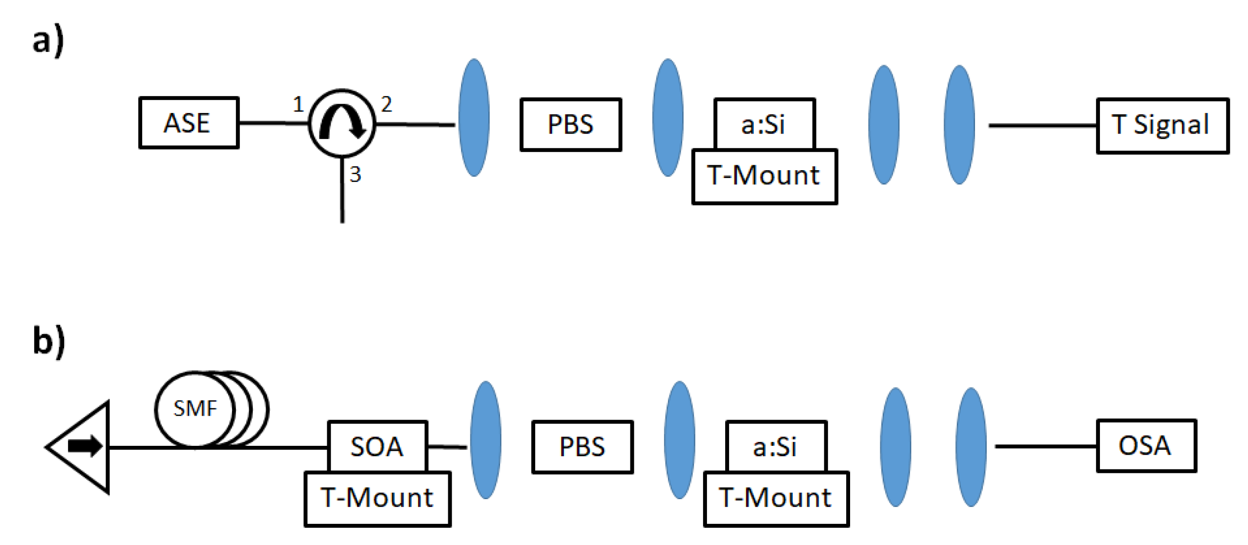
3. Optical Characterization Measurement Results
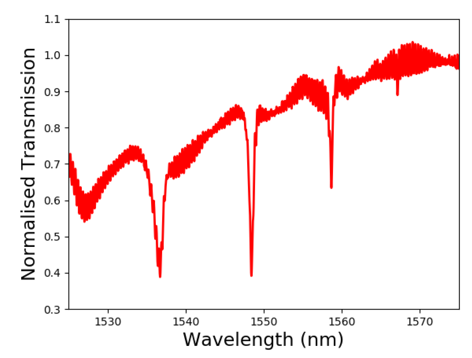
3.1. Photonic Crystal Transmission Spectra
Optical characterization of the a-Si PhC cavities was performed using an end-fire measurement set up; see Figure 3 for schematic. To measure the optical transmission spectra of the PhC cavities a broadband Amplified Spontaneous Emission (ASE) source (Amonics ALS-CL-15-B-FA, https://www.amonics.com/product/39). was coupled to the polymer waveguide over the a-Si PhC cavity via a circulator, free-space optics and polarizing beam splitter. Light transmitted through the PhC cavity was collected from the polymer waveguide after propagation through the second lens system. Optical power was measured on a power meter and optical spectra were measured on an optical spectrum analyzer with a spectral resolution of . Temperature of the a-Si PhC cavity was maintained at by an external temperature controller.
Figure 3.
(a) End-fire set up used to characterize PhC cavity transmission and reflection spectra. (b) End-fire set up used to characterize operation of hybrid external cavity laser.
Measurements of the transmission spectra of the PhC cavities show that resonances occur in the C and L bands relevant for optical telecommunications, see Figure 4. Spectrum of the PhC cavity with lattice spacing of nm shows resonant reflection taking place at and nm with measured Q-factors of and 1176 respectively.
Figure 4.
Measured optical transmission spectrum of the PhC cavity with lattice spacing nm. The PhC cavity Free Spectral Range (FSR) is greater than nm.
Measurement of the DA PhC cavity transmission spectra show that multiple resonances can be obtained and that the position of these resonances varies with the PhC lattice constant; see Figure 5. Shift in resonance wavelengths with PhC lattice constants show that it is possible to have fine control over optical characteristics of the a-Si PhC cavity. Given the level of control that is available it should be possible to deploy a-Si PhC cavity in a wavelength-division multiplexing (WDM) application. Linear fits of the resonant wavelength versus PhC lattice constant data for each mode show that the average slope of the fits is computed to be . The average measured Q-factor for the resonances shown in Figure 5 is , but measured Q-factors as high as can be obtained; see Figure 4. In [15] it was reported that a similar DA PhC with lattice constant of nm fabricated on c-Si had resonant wavelengths at nm and nm, it can be seen from Figure 5 that for the same DA PhC with the same lattice constant, but different hole radius, the a-Si PhC has resonant wavelengths at nm and nm, the variation in resonant wavelengths for the DA PhC can be attributed to different hole radius values, nm in the case of c-Si and nm in the case of a-Si, and differences in refractive index between a-Si and c-Si.
Figure 5.
Measured resonant wavelengths of the PhC cavity and their variation with PhC lattice constant spacing. For each of the modes it is observed that .
3.2. Hybrid External Cavity Laser Operation
An external cavity laser is set up using a variation of the end-fire measurement system, see Figure 3. A commercial, packaged SOA (Kamelian SOA OPA-20-N-C-F-A) is used as the laser gain medium, lenses are used to couple the broadband SOA output to the a-Si PhC cavity which acts as a wavelength selective mirror, and a retro-reflector coupled to standard single-mode fibre (Thorlabs P5-SMF28ER-P01-1) is used to form the second mirror of the laser cavity. The length of the cavity in this instance is determined by the length of the fibre pigtails on the commercial SOA and the spacing between the lenses that couple light from the SOA to the a-Si chip. Since the PhC acts as a wavelength selective mirror only light with wavelength within the PhC resonance bandwidth gets reflected from the PhC back into the SOA. As the wavelength selected by the PhC mirror propagates in the SOA it is amplified. Further details concerning the operation of this type of laser can be found in [15]. The temperature of the SOA and the PhC cavity were separately maintained at a constant temperature of . The SOA used in these measurements has a gain spectrum peak at nm.
The power–current characteristic for the laser with lattice spacing of nm was measured using an optical power meter; see Figure 6. After correcting for the lens system insertion losses, approximately dB, the laser is seen to output optical power of for of current across the SOA, which is more than double the output power observed in a similar system reported in [15] where of output power was measured for of SOA current. The laser threshold current is approximately and is typical for lasers of this type; in [15] a threshold current of is reported. The slope efficiency of the laser above threshold is .
Figure 6.
Measured Light-Current (LI) curve for the external cavity laser. Can see that threshold current is approximately and the output power from the laser is at for RSOA (Reflective Semiconductor Optical Amplifier) current. Slope efficiency of the laser is .
The optical spectrum of the laser output was measured on an Optical Spectrum Analyser (OSA) for several samples with different lattice spacings. Figure 7 shows the measured optical spectrum of three lasers with PhC cavity lattice spacings of and operating in a single-mode regime with wavelengths of and respectively. Observed lasing wavelengths are consistent with the measured PhC cavity resonant wavelengths shown in Figure 4 and Figure 5. The side-mode suppression ratio (SMSR) in each case is . The current across the SOA in each case was , and with the retro-reflector in place the SOA output power at this current was .
Figure 7.
Measured optical spectra of external cavity lasers with PhC cavity lattice spacings of and . The lasers are operating at wavelengths of and with SMSR of and respectively.
Single-mode operation of the lasers was not maintained as the SOA current increased. Figure 8 shows spectral broadening of the laser line as the SOA current increased from to . The spectrum bandwidth increased from at to at . The data shown in Figure 8 is for the PhC sample with lattice spacing of , and similar behavior was observed with the other samples. Broadening is caused by the simultaneous lasing of multiple lines within the laser cavity. In a cavity of length the longitudinal mode spacing was approximately . The bandwidth of the PhC resonances was approximately which means that there were many modes available for lasing. As the SOA current increased every longitudinal cavity mode present in the resonance peak bandwidth had enough amplification to win over total round-trip losses, even if they were reflected less compared with the main peak; this lead to very fast switching of the lasing mode between the available cavity modes, which was then captured by the time-averaged spectra on the OSA, whose resolution was limited to , as spectral broadening.
Figure 8.
Observed ASE broadening caused by narrow longitudinal mode spacing of external laser cavity. The PhC lattice constant in this case is .
When the current increases further, the gain is so high that even other resonances with lower Q factors are in an over-threshold condition and all the cavity modes overlapping with these resonances start lasing. In particular, it can be seen that a PhC resonance of around , shown in Figure 4, starts lasing for SOA currents greater than .
4. Conclusions
Dispersion-adapted PhC cavities of length were fabricated on a low-temperature, CMOS compatible a-Si platform. The fabrication process was optimized to ensure a high-uniformity of hole diameters and smooth sidewalls. A low-loss polymer waveguide was formed on top of the PhC cavity to optimize optical coupling to the PhC cavity.
Measurements of the transmission spectra of the PhC cavities show that the PhC exhibit resonant reflections in the C and L wavelength bands relevant for optical telecommunications. Data shows that it is possible to obtain PhC cavities with Q-factors as high as 15,862. Data shows that is is also possible to achieve lithographic control over the positions of the resonant wavelengths by careful choice of the PhC lattice constant.
Measurement of the optical spectrum of the hybrid external cavity photonic crystal laser shows that it is possible to operate this laser in a single-mode configuration with SMSR of . Unfortunately, it was not possible to maintain single-mode operation due to the length of the cavity used to make the hybrid external cavity laser. To ensure single-mode operation, the length of the laser cavity would need to be reduced to the range of millimetres. This could be achieved by packaging the a-Si PhC reflector with an RSOA gain chip whose length is on the order of .
Author Contributions
Conceptualization, investigation and validation, S.I., C.D., A.L., R.S. and L.O.; formal analysis, S.I., C.D., R.S. and L.O.; writing-original draft preparation, S.I., R.S.; writing-review and editing, S.I., R.S. and L.O.; supervision and project administration, L.O.; funding acquisition, C.D., R.S. and L.O. All authors have read and agreed to the published version of the manuscript.
Funding
The authors gratefully acknowledge the following funding sources EU ERC-SG 337508 DANCER, EU H2020 Marie Skłodowska-Curie 713654 and SFI 18/TIDA/6128.
Conflicts of Interest
The authors declare no conflict of interest.
Abbreviations
The following abbreviations are used in this manuscript:
| a-Si | Amorphous Silicon |
| a-Si:H | Hydrogenated Amorphous Silicon |
| c-Si | Crystalline Silicon |
| CMOS | Complementary metal–oxide–semiconductor |
| DA | Dispersion Adapted |
| SOG | Spin-On-Glass |
| PhC | Photonic Crystal |
| SEM | Scanning Electron Microscope |
| SMSR | Side-Mode Supression Ratio |
| SOA | Semiconductor Optical Amplifier |
| SOI | Silicon-On-Insulator |
References
- Cisco. Visual Networking Index Forecast 2019. Available online: https://bit.ly/2TYstY8 (accessed on 22 November 2019).
- Zhong, K.; Zhou, X.; Huo, J.; Yu, C.; Lu, C.; Lau, A.P.T. Digital signal processing for short-reach optical communications: A review of current technologies and future trends. J. Lightwave Technol. 2018, 36, 377–400. [Google Scholar] [CrossRef]
- Alexoudi, T.; Terzenidis, N.; Pitris, S.; Moralis-Pegios, M.; Maniotis, P.; Vagionas, C.; Mitsolidou, C.; Mourgias-Alexandris, G.; Kanellos, G.T.; Miliou, A.; et al. Optics in computing: From photonic network-on-chip to chip-to-chip interconnects and disintegrated architectures. J. Lightwave Technol. 2019, 37, 363–379. [Google Scholar] [CrossRef]
- Krishnamoorthy, A.V.; Thacker, H.D.; Torudbakken, O.; Müller, S.; Srinivasan, A.; Decker, P.J.; Opheim, H.; Cunningham, J.E.; Shubin, I.; Zheng, X.; et al. From chip to cloud: Optical interconnects in engineered systems. J. Lightwave Technol. 2017, 35, 3103–3115. [Google Scholar] [CrossRef]
- Cheng, Q.; Bahadori, M.; Glick, M.; Rumley, S.; Bergman, K. Recent advances in optical technologies for data centers: A review. Optica 2018, 5, 1354–1370. [Google Scholar] [CrossRef]
- Van Campenhout, J.; Ban, Y.; De Heyn, P.; Srinivasan, A.; De Coster, J.; Lardenois, S.; Snyder, B.; Balakrishnan, S.; Lepage, G.; Golshani, N.; et al. Silicon photonics for 56G NRZ optical interconnects. In Proceedings of the 2018 Optical Fiber Communications Conference and Exposition (OFC), San Diego, CA, USA, 11–15 March 2018; pp. 1–3. [Google Scholar]
- Lee, Y.H.D.; Lipson, M. Back-end deposited silicon photonics for monolithic integration on CMOS. IEEE Sel. Top. Quant. Electron. 2012, 19, 8200207. [Google Scholar] [CrossRef]
- Liu, A.; Jones, R.; Liao, L.; Samara-Rubio, D.; Rubin, D.; Cohen, O.; Nicolaescu, R.; Paniccia, M. A high-speed silicon optical modulator based on a metal–oxide–semiconductor capacitor. Nature 2004, 427, 615. [Google Scholar] [CrossRef] [PubMed]
- Oo, S.; Tarazona, A.; Petra, R.; Khokhar, A.; Reed, G.; Peacock, A.; Chong, H. Hot-wire CVD a-Si: H for low loss silicon photonic waveguides. In Proceedings of the 2018 Conference on Lasers and Electro-Optics Pacific Rim (CLEO-PR), Hong Kong, China, 29 July–3 August 2018; pp. 1–2. [Google Scholar]
- Lipka, T.; Moldenhauer, L.; Müller, J.; Trieu, H.K. Energy-efficient wavelength multiplexers based on hydrogenated amorphous silicon resonators. IEEE Photonics J. 2015, 7, 1–11. [Google Scholar] [CrossRef]
- Lipka, T.; Moldenhauer, L.; Müller, J.; Trieu, H.K. Photonic integrated circuit components based on amorphous silicon-on-insulator technology. Photonics Res. 2016, 4, 126–134. [Google Scholar] [CrossRef]
- Della Corte, F.G.; Rao, S. Use of amorphous silicon for active photonic devices. IEEE Trans. Electron. Dev. 2013, 60, 1495–1505. [Google Scholar] [CrossRef]
- Rao, S.; Della Corte, F. Numerical analysis of electro-optical modulators based on the amorphous silicon technology. J. Lightwave Technol. 2014, 32, 2399–2407. [Google Scholar] [CrossRef]
- Ferrotti, T.; Duprez, H.; Jany, C.; Chantre, A.; Seassal, C.; Bakir, B.B. O-Band III–V-on-Amorphous-Silicon Lasers Integrated With a Surface Grating Coupler. IEEE Photonics Technol. Lett. 2016, 28, 1944–1947. [Google Scholar] [CrossRef]
- Liles, A.A.; Debnath, K.; O’Faolain, L. Lithographic wavelength control of an external cavity laser with a silicon photonic crystal cavity-based resonant reflector. Opt. Lett. 2016, 41, 894–897. [Google Scholar] [CrossRef] [PubMed]
- Debnath, K.; Welna, K.; Ferrera, M.; Deasy, K.; Lidzey, D.G.; O’Faolain, L. Highly efficient optical filter based on vertically coupled photonic crystal cavity and bus waveguide. Opt. Lett. 2013, 38, 154–156. [Google Scholar] [CrossRef] [PubMed]
- Welna, K.; Portalupi, S.L.; Galli, M.; O’Faolain, L.; Krauss, T.F. Novel dispersion-adapted photonic crystal cavity with improved disorder stability. IEEE J. Quant. Electron. 2012, 48, 1177–1183. [Google Scholar] [CrossRef]
- Zilkie, A.; Seddighian, P.; Bijlani, B.; Qian, W.; Lee, D.; Fathololoumi, S.; Fong, J.; Shafiiha, R.; Feng, D.; Luff, B.; et al. Power-efficient III-V/Silicon external cavity DBR lasers. Opt. Express 2012, 20, 23456–23462. [Google Scholar] [CrossRef] [PubMed]
- Alonso, J.; Ramirez, S.; Garcia, M.; Ortiz, A. High rate–low temperature deposition of silicon dioxide films by remote plasma enhanced chemical vapor deposition using silicon tetrachloride. J. Vac. Sci. Technol. A Vac. Surf. Films 1995, 13, 2924–2929. [Google Scholar] [CrossRef]
- White, T.; O’Faolain, L.; Li, J.; Andreani, L.; Krauss, T. Silica-embedded silicon photonic crystal waveguides. Opt. Express 2008, 16, 17076–17081. [Google Scholar] [CrossRef] [PubMed]
© 2019 by the authors. Licensee MDPI, Basel, Switzerland. This article is an open access article distributed under the terms and conditions of the Creative Commons Attribution (CC BY) license (http://creativecommons.org/licenses/by/4.0/).