A Comparison between Anodizing and EBSD Techniques for Primary Particle Size Measurement


Abstract
1. Introduction
2. Materials and Methods
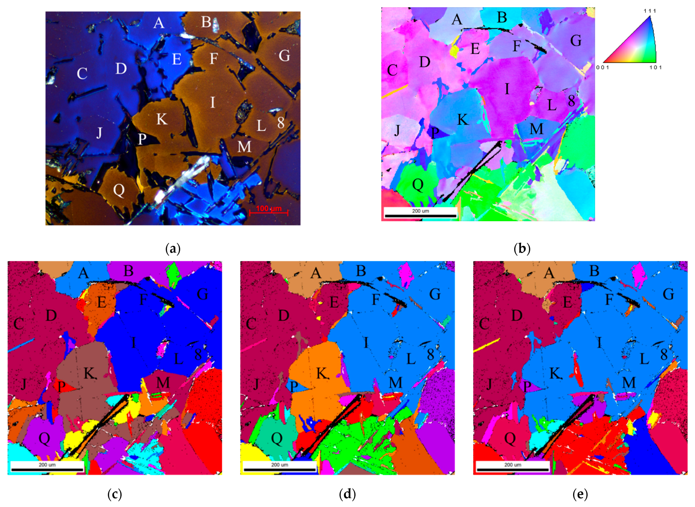
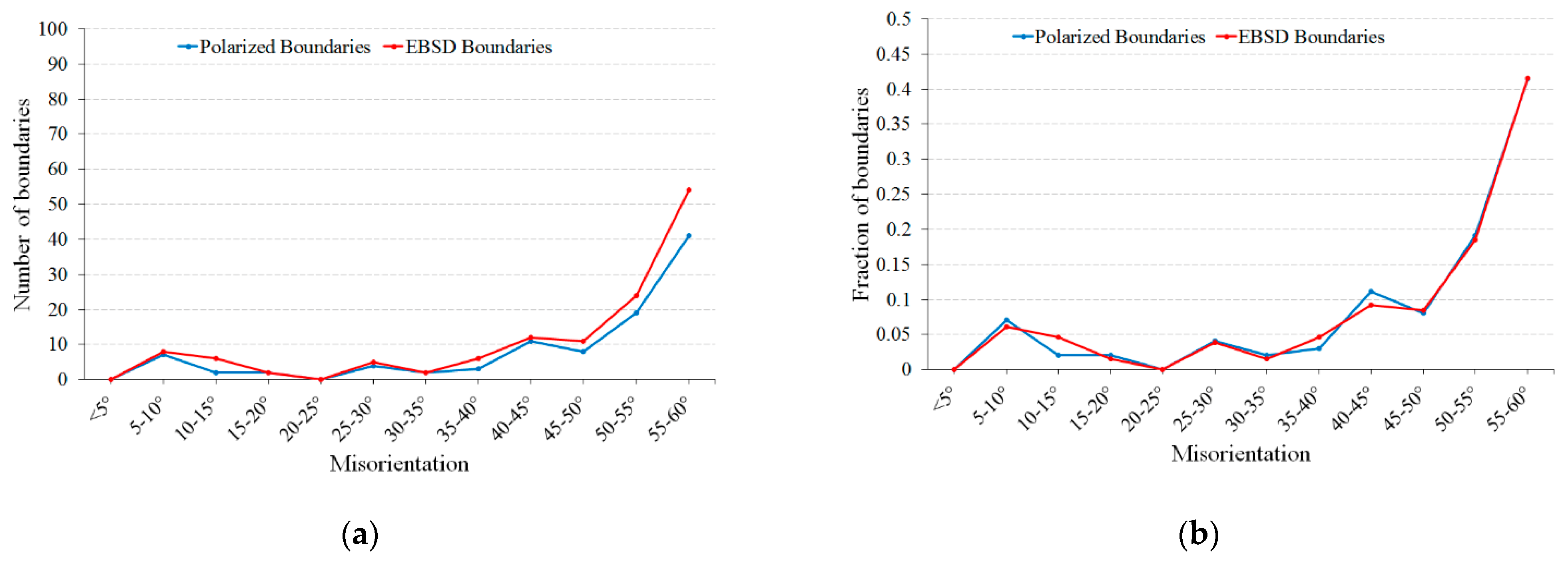
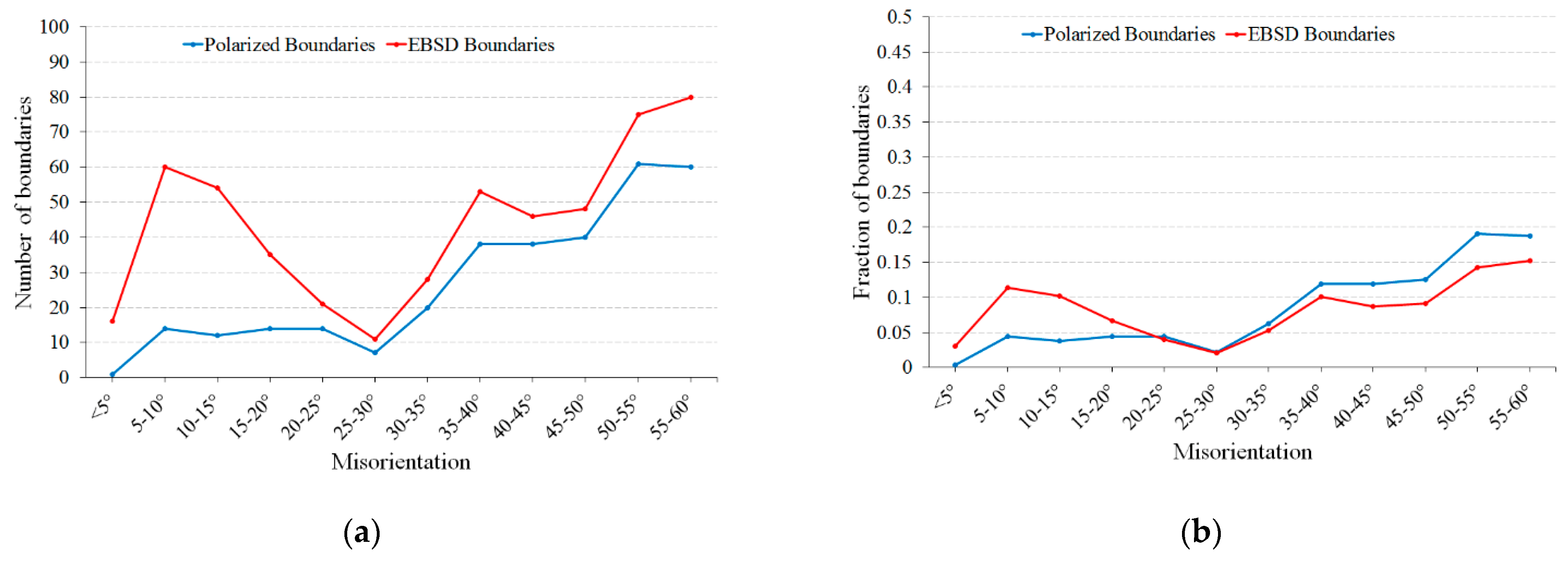
3. Results and Discussions
4. Conclusions
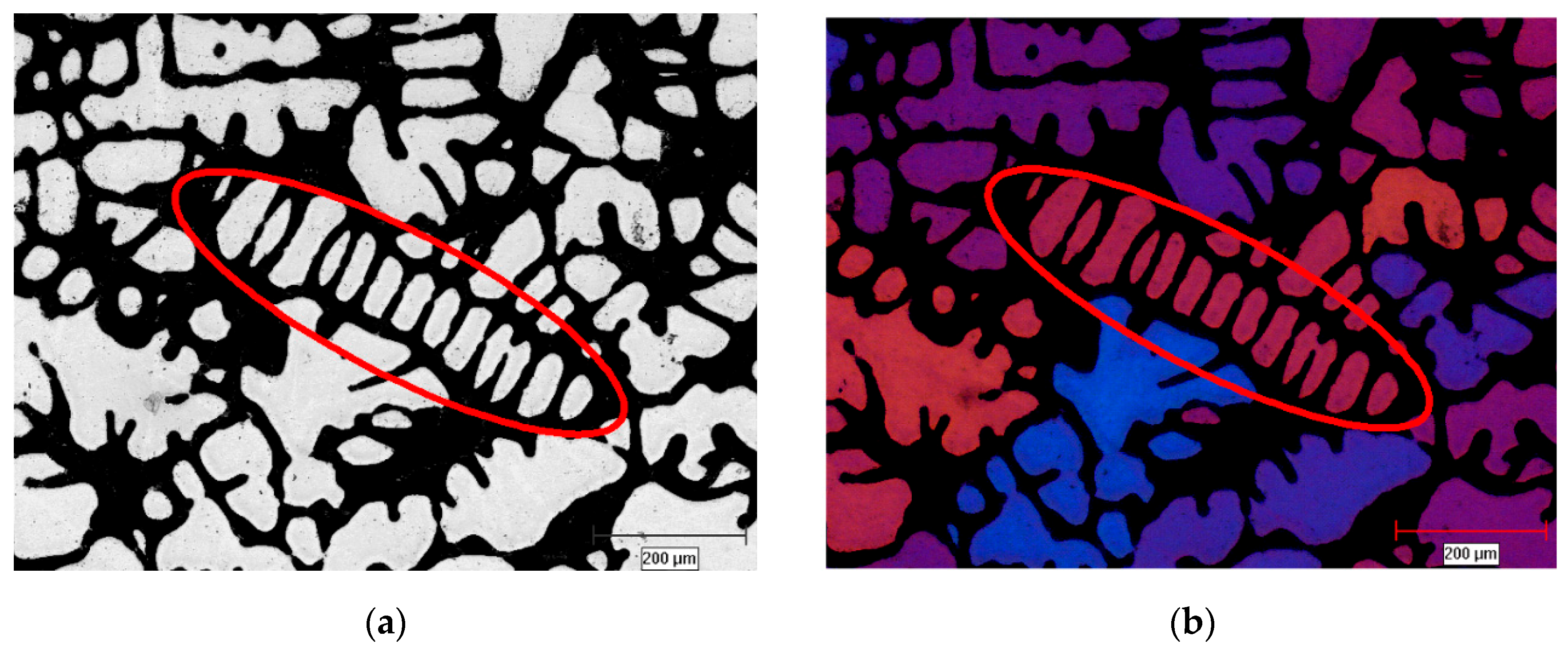
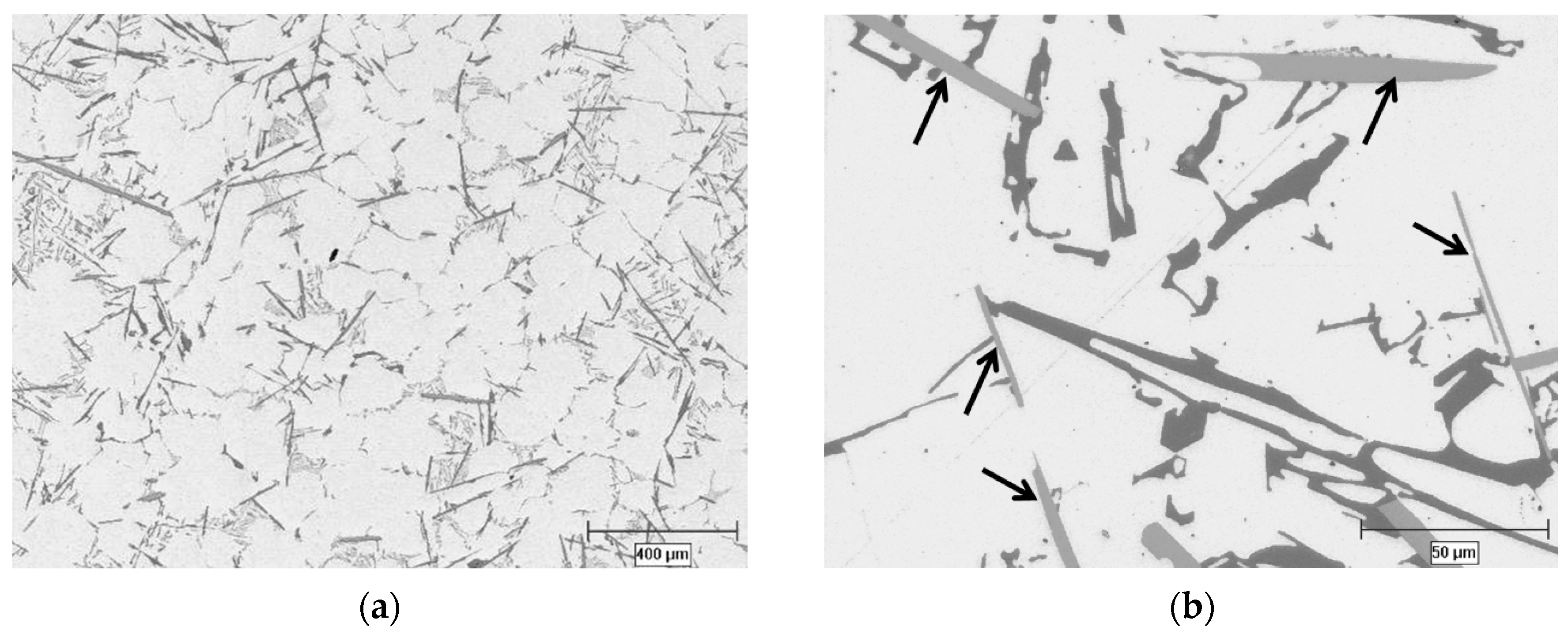
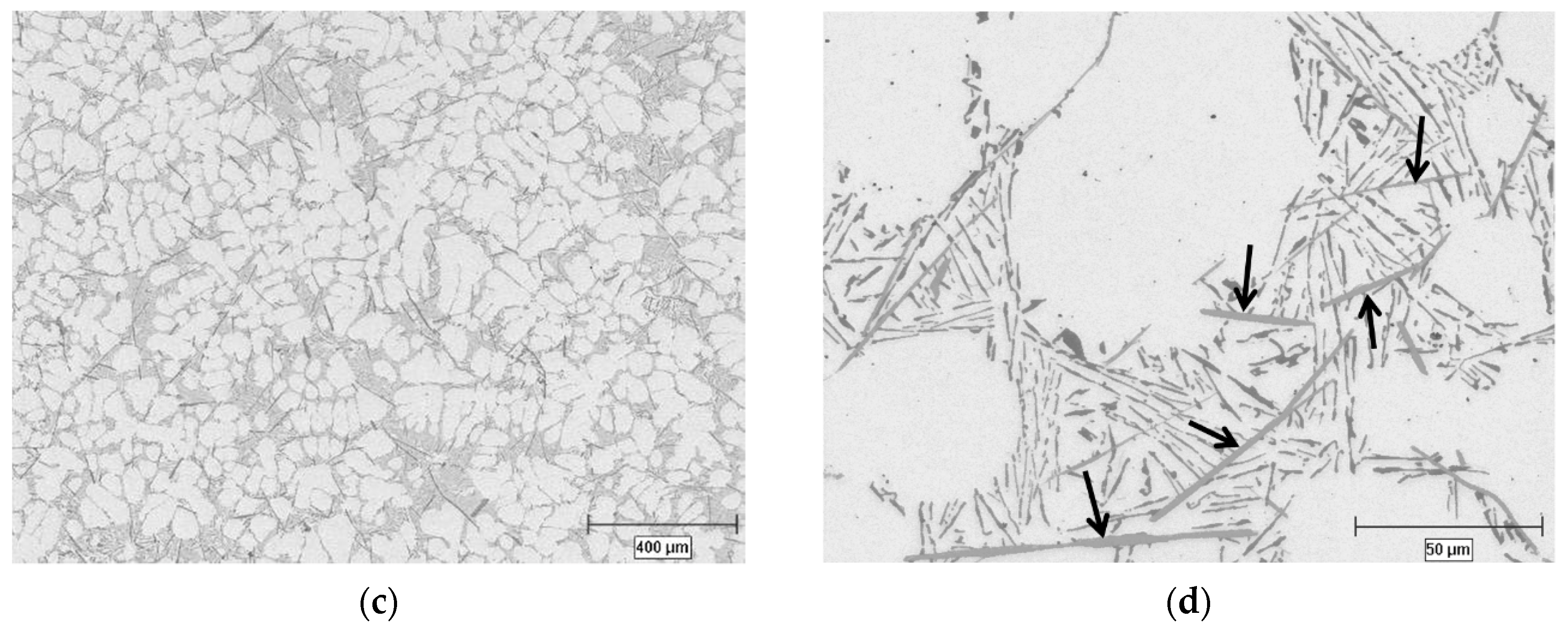
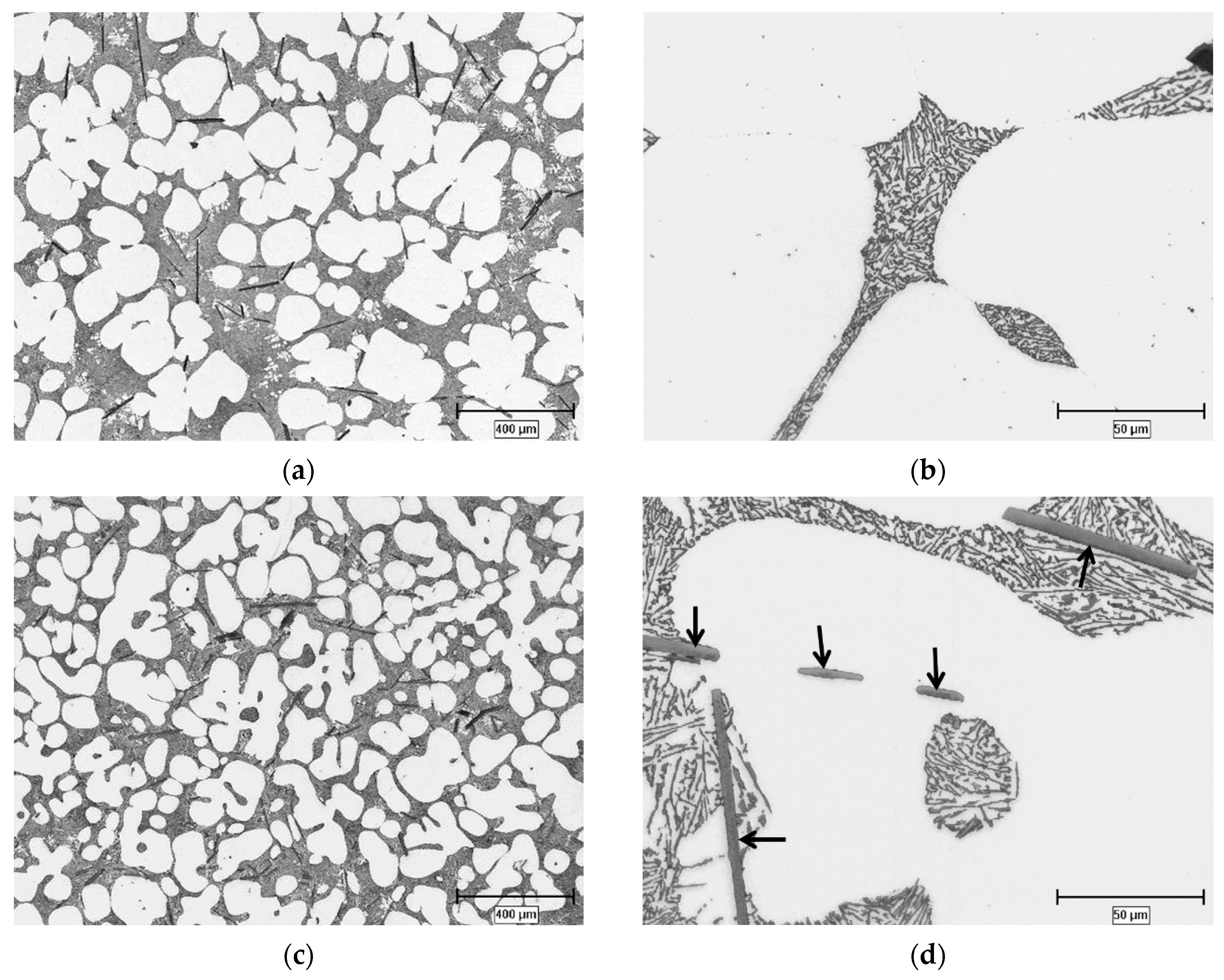
- Anodizing-polarized light microscopy combination is a reliable characterization method for microstructural analysis of as-cast alloys.
- Color metallography is a faster and more cost-effective method for microstructural analysis of as-cast alloys, although more data is acquired through EBSD analysis.
- It was found that a 10 degree misorientation criterion is an acceptable misorientation level for EBSD grain mapping.
- The number and fraction of grain boundaries detected and resolved for both techniques are basically the same and have similar trend when plotted against the degree of grain misorientation.
Author Contributions
Funding
Acknowledgments
Conflicts of Interest
References
- Nafisi, S.; Ghomashchi, R. Semi-Solid Processing of Aluminum Alloys; Springer: Berlin, Germany, 2016; ISBN 978-3-319-40333-5. [Google Scholar]
- Niroumand, B.; Xia, K. 3D Study of the Structure of Primary Crystals in a Rheocast Al-Cu Alloy. Mater. Sci. Eng. A 2000, 283, 70–75. [Google Scholar] [CrossRef]
- Ito, Y.; Flemings, M.C.; Cornie, J.A. Rheological Behavior and Microstructure of Al-6.5 wt % Si Alloy. In Nature and Properties of Semi-Solid Materials; Sekhar, J.A., Dantzig, J., Eds.; TMS: Warrendale, PA, USA, 1991; pp. 3–17. [Google Scholar]
- Suery, M. Mise en forme des alliages métalliques à l’état semi-solide; Lavoisier Publication: Paris, France, 2002. [Google Scholar]
- Limodin, N.; Salvo, L.; Suery, M.; DiMichiel, M. In situ and real-time 3-D microtomography investigation of dendritic solidification in an Al–10 wt.% Cu alloy. Acta Mater. 2009, 57, 2300–2310. [Google Scholar] [CrossRef]
- Xu, W.; Ferry, M.; Mateescu, N.; Cairney, J.M.; Humphreys, F.J. Techniques for generating 3-D EBSD microstructures by FIB tomography. Mater. Charact. 2007, 58, 961–967. [Google Scholar] [CrossRef]
- Zaafarani, Z.; Raabe, D.; Singh, R.N.; Roters, F.; Zaefferer, S. Three-dimensional investigation of the texture and microstructure below a nanoindent in a Cu single crystal using 3D EBSD and crystal plasticity finite element simulations. Acta Mater. 2006, 54, 1863–1876. [Google Scholar] [CrossRef]
- Voort, G.V. Metallography, Principles and Practice; ASM International: New York, NY, USA, 1999. [Google Scholar]
- Voort, G.V. ASM Handbook, Volume 09: Metallography and Microstructures; ASM International: Materials Park, OH, USA, 2004. [Google Scholar]
- Oxford Instruments. Available online: www.ebsd.com (accessed on 25 April 2019).
- OIM Analysis Tutorials, Ametek Inc. Available online: www.edax.com (accessed on 25 April 2019).
- Vander Voort, G.F. Metallographic specimen preparation for electron backscattered diffraction. Part I. Pract. Metallogr. 2011, 48, 454–473. [Google Scholar] [CrossRef]
- Vander Voort, G.F. Metallographic specimen preparation for electron backscattered diffraction. Part II. Pract. Metallogr. 2011, 48, 527–543. [Google Scholar]
- Nafisi, S.; Ghomashchi, R. Microstructural Evolution of Electromagnetically Stirred Feedstock SSM Billets during Reheating Process. Metall. Microstruct. Anal. 2013, 2, 96–106. [Google Scholar] [CrossRef]
- Flemings, M.C. Behavior of metal alloys in the semi-solid state. Metal. Trans. A 1991, 22, 952–981. [Google Scholar] [CrossRef]
- Kirkwood, D.H. Semisolid metal processing. Int. Mater. Rev. 1994, 39, 173–189. [Google Scholar] [CrossRef]
- Fan, Z. Semisolid metal processing. Int. Mater. Rev. 2002, 47, 49–85. [Google Scholar] [CrossRef]
- Nafisi, S.; Emadi, D.; Shehata, M.T.; Ghomashchi, R. Effects of Electromagnetic Stirring and Superheat on the Microstructural Characteristics of Al-Si-Fe Alloy. Mater. Sci. Eng. A 2006, 432, 71–83. [Google Scholar] [CrossRef]


| Process Parameter | Color Metallography (minutes) | EBSD (minutes) |
|---|---|---|
| Sample Preparation | 20 | 50 |
| Anodizing | 10 (per sample) | - |
| Optical Microscopy | 10 (per sample) | - |
| EBSD | - | 75 (per scan) |
| Post-processing of Results | - | 15 (per scan) |
| Total | 40 | 140 |
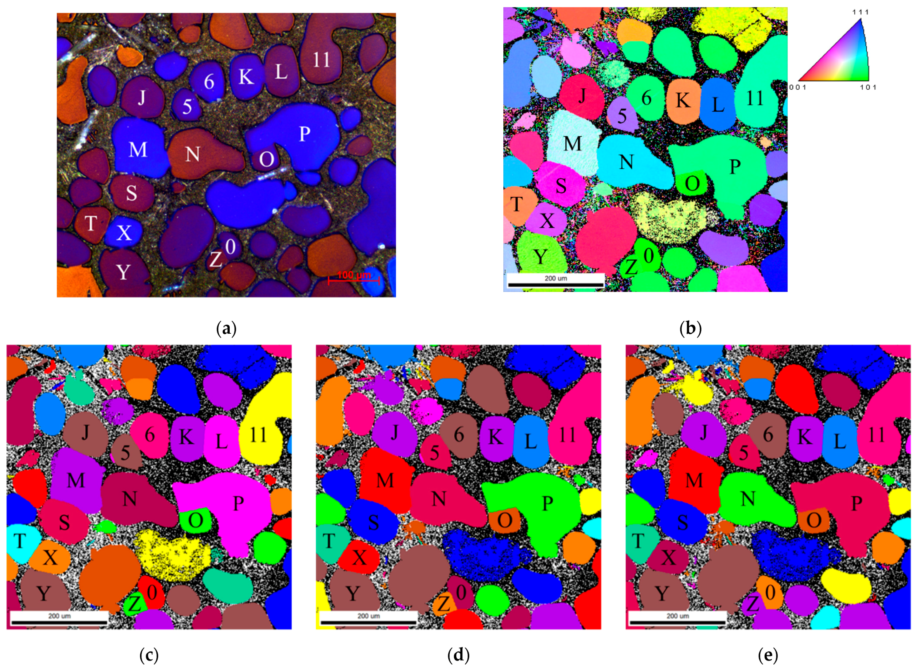
| Grain Boundary | Misorientation | EBSD 5° Misorientation | EBSD 10° Misorientation | EBSD 15° Misorientation | Color Metallography |
|---|---|---|---|---|---|
| KL | 55.6 | Y | Y | Y | Y |
| JM | 32.7 | Y | Y | Y | Y |
| MN | 55.6 | Y | Y | Y | Y |
| MS | 42.3 | Y | Y | Y | Y |
| TX | 29.8 | Y | Y | Y | Y |
| XY | 43 | Y | Y | Y | Y |
| OP | 59.3 | Y | Y | Y | Y |
| Z0 | 58.7 | Y | Y | Y | Y |
| L 11 | 38.3 | Y | Y | Y | Y |
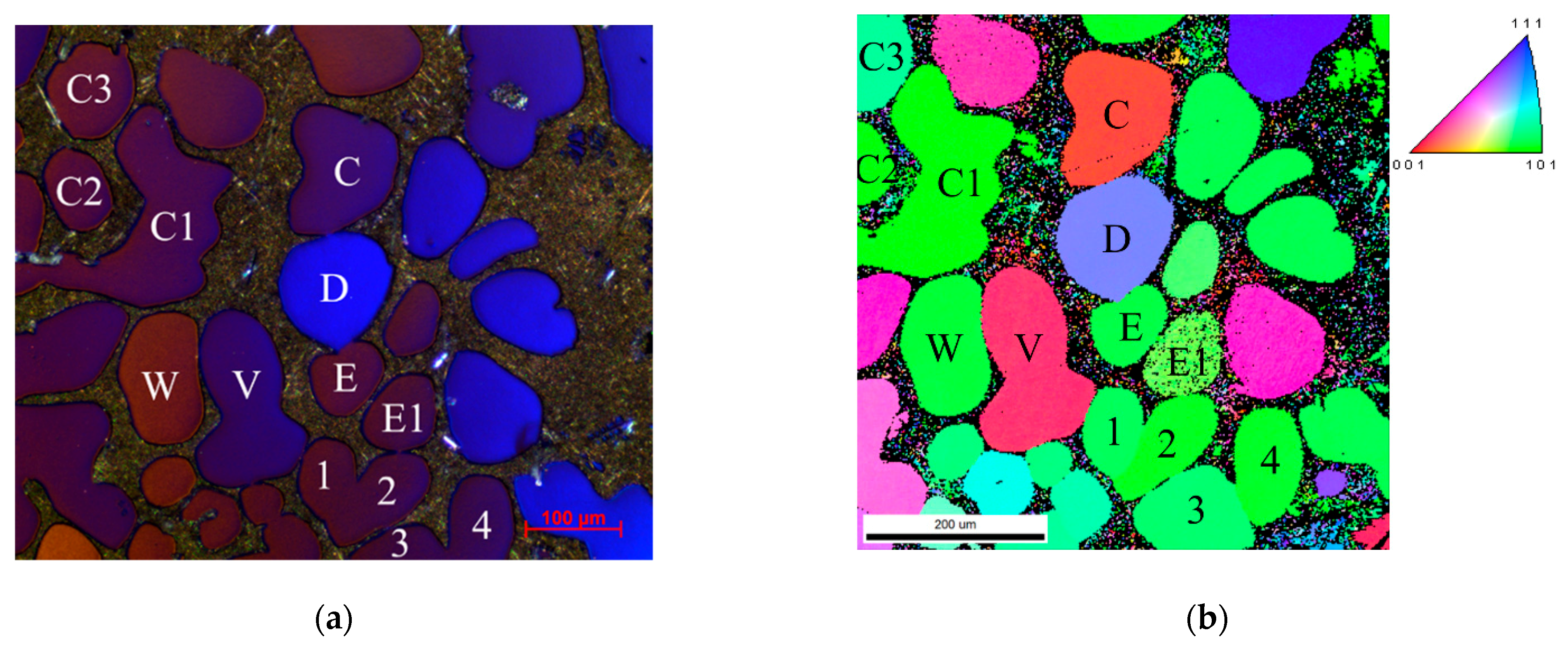
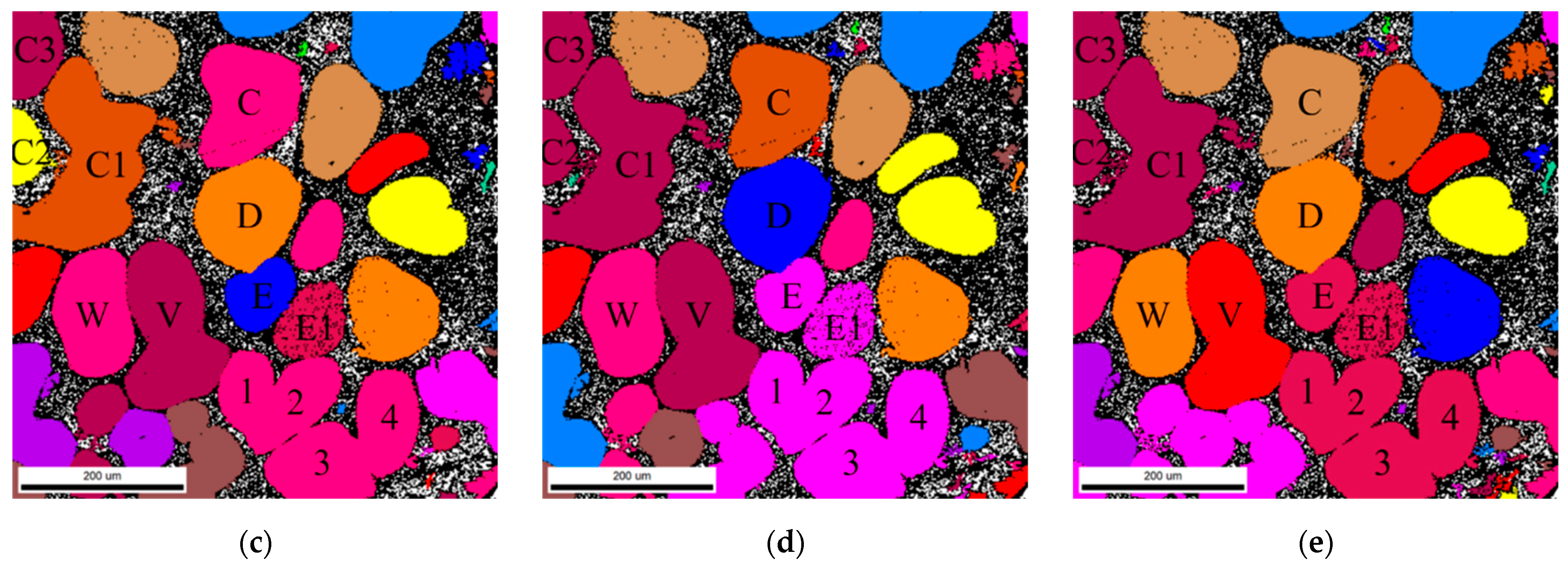
| Grain Boundary | Misorientation | EBSD 5° Misorientation | EBSD 10° Misorientation | EBSD 15° Misorientation | Color Metallography |
|---|---|---|---|---|---|
| CD | 58 | Y | Y | Y | Y |
| DE | 51.6 | Y | Y | Y | Y |
| VW | 38.4 | Y | Y | Y | Y |
| 1 2 | 2.4 | N | N | N | N |
| 3 4 | 4.2 | N | N | N | N |
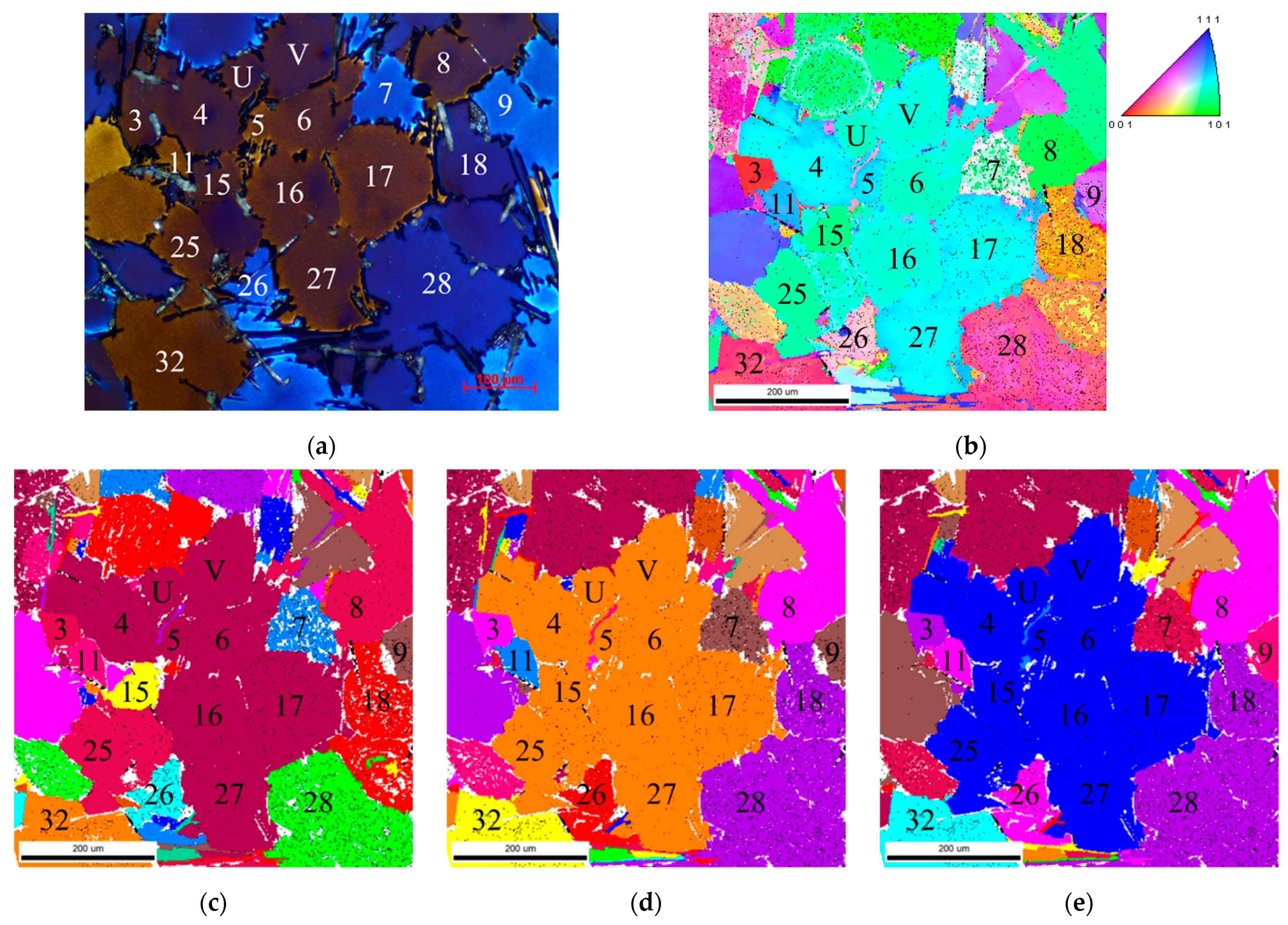
| Grain Boundary | Misorientation | EBSD 5° Misorientation | EBSD 10° Misorientation | EBSD 15° Misorientation | Color Metallography |
|---|---|---|---|---|---|
| UV | 2.9 | N | N | N | N |
| U4 | 6.8 | N | N | N | N |
| U5 | 8.4 | N | N | N | N |
| V5 | 5.9 | N | N | N | N |
| V6 | 3.8 | N | N | N | N |
| 3 11 | 58.5 | Y | Y | Y | Y |
| 3 4 | 55.8 | Y | Y | Y | N |
| 4 5 | 10.2 | N | N | N | N |
| 4 15 | 10.3 | Y | N | N | N |
| 4 11 | 35.6 | Y | Y | Y | Y |
| 5 6 | 5 | N | N | N | N |
| 5 15 | 12.3 | Y | N | N | N |
| 5 16 | 3.4 | N | N | N | N |
| 6 7 | 55.3 | Y | Y | Y | Y |
| 6 16 | 2.3 | N | N | N | N |
| 6 17 | 8.3 | N | N | N | N |
| 7 8 | 50.9 | Y | Y | Y | Y |
| 7 17 | 55.8 | Y | Y | Y | Y |
| 8 9 | 53 | Y | Y | Y | Y |
| 8 18 | 43.9 | Y | Y | Y | Y |
| 9 18 | 60 | Y | Y | Y | Y |
| 11 15 | 28.2 | Y | Y | Y | Y |
| 15 16 | 8.4 | Y | N | N | N |
| 15 25 | 4 | Y | N | N | N |
| 16 17 | 6.5 | N | N | N | N |
| 16 27 | 3.7 | N | N | N | N |
| 16 26 | 41.3 | Y | Y | Y | Y |
| 17 18 | 44.8 | Y | Y | Y | Y |
| 17 28 | 51 | Y | Y | Y | Y |
| 18 28 | 14.7 | Y | N | N | N |
| 25 26 | 40.9 | Y | Y | Y | Y |
| 26 27 | 41.8 | Y | Y | Y | Y |
| 27 28 | 53.2 | Y | Y | Y | Y |
| Grain Boundary | Misorientation | EBSD 5° Misorientation | EBSD 10° Misorientation | EBSD 15° Misorientation | Color Metallography |
|---|---|---|---|---|---|
| AB | 34.1 | Y | Y | Y | Y |
| AE | 53.4 | Y | Y | Y | N |
| AD | 53.1 | Y | Y | Y | N |
| BF | 21.7 | Y | N | N | N |
| BE | 39.6 | Y | Y | Y | Y |
| CD | 5.3 | N | N | N | N |
| DE | 8.2 | Y | N | N | N |
| DJ | 4.8 | N | N | N | N |
| DK | 52.2 | Y | Y | Y | Y |
| DI | 43.1 | Y | Y | Y | Y |
| EI | 43.4 | Y | Y | Y | Y |
| EF | 49.4 | Y | Y | Y | Y |
| FG | 8.8 | N | N | N | N |
| GL | 6.4 | N | N | N | N |
| G8 | 10.3 | N | N | N | N |
| IL | 3.9 | N | N | N | N |
| IK | 15.2 | Y | Y | N | N |
| IM | 14 | Y | N | N | N |
| KP | 19.6 | Y | Y | Y | Y |
| KQ | 36.2 | Y | Y | Y | N |
| LM | 11.4 | Y | N | N | N |
| L8 | 6.8 | N | N | N | N |
© 2019 by the authors. Licensee MDPI, Basel, Switzerland. This article is an open access article distributed under the terms and conditions of the Creative Commons Attribution (CC BY) license (http://creativecommons.org/licenses/by/4.0/).
Share and Cite
Nafisi, S.; Roccisano, A.; Ghomashchi, R.; Vander Voort, G. A Comparison between Anodizing and EBSD Techniques for Primary Particle Size Measurement. Metals 2019, 9, 488. https://doi.org/10.3390/met9050488
Nafisi S, Roccisano A, Ghomashchi R, Vander Voort G. A Comparison between Anodizing and EBSD Techniques for Primary Particle Size Measurement. Metals. 2019; 9(5):488. https://doi.org/10.3390/met9050488
Chicago/Turabian StyleNafisi, Shahrooz, Anthony Roccisano, Reza Ghomashchi, and George Vander Voort. 2019. "A Comparison between Anodizing and EBSD Techniques for Primary Particle Size Measurement" Metals 9, no. 5: 488. https://doi.org/10.3390/met9050488
APA StyleNafisi, S., Roccisano, A., Ghomashchi, R., & Vander Voort, G. (2019). A Comparison between Anodizing and EBSD Techniques for Primary Particle Size Measurement. Metals, 9(5), 488. https://doi.org/10.3390/met9050488