Abstract
Within a power hardware-in-the-loop (PHIL) controller design automation (CDA) framework for voltage feedback grid-forming inverters, a scaled-down inverter system is developed for time-domain response solving. This hardware-based approach effectively addresses the conflicting demands of accuracy, computational efficiency, and modeling cost that are commonly encountered in simulation-based methods. Conventional synchronous sampling in digitally controlled pulse-width modulation (PWM) inverters introduces severe low-frequency distortion and significant ripple components in the step response, leading to non-decaying oscillations that compromise the extraction of settling time and steady-state error. By analyzing the sideband aliasing mechanism in capacitor-voltage sampling and associated harmonic-cancellation conditions, aliasing-free sampling is achieved using 90° phase-shifted anti-aliasing filters combined with synchronous sampling. Although Fast Fourier Transform (FFT) filtering offers the highest fidelity, it suffers from window-boundary distortions and is unsuitable for online use; therefore, four practical filtering schemes are evaluated against the FFT benchmark, among which oversampling with moving-average filtering (MAF) retains dynamics closest to the FFT result while avoiding its distortions. An objective function incorporating step-response metrics is constructed to optimize single-variable active damping and multiple resonant controllers, mitigating severe overshoot encountered in conventional integral-based approaches. Experimental results verify the aliasing mechanism and the effectiveness of the proposed CDA method.
1. Introduction
Power electronic (PE) systems are extensively used in key applications like renewable energy integration, where control design is crucial to meeting performance goals [1]. Traditional PE controller design typically relies on iterative trial-and-error processes [2] involving repeated modeling, parameter tuning, and experimental validation. This approach often suffers from long development cycles, high resource consumption, and a strong dependence on expert experience, making it increasingly incompatible with the modern demand for low-cost and highly efficient optimization. Thus, an effective CDA tool is urgently needed to meet two crucial requirements: (1) the capacity to converge toward the global optimum while quickly exploring enormous design spaces (DSs); (2) the capacity to guarantee system resilience, stability, and transient performance under dynamic operating circumstances and manufacturing tolerances.
In power electronic inverter systems, grid-following inverters (GFL) and grid-forming inverters (GFM) are the two primary types widely adopted [3]. GFL inverters regulate the AC side current by tracking the phase angle of the grid voltage through a phase-locked loop (PLL) [4]. It enables distortion-free control and ripple-free signal acquisition from PWM-modulated current signals with relative ease. In contrast, GFM inverters directly control the voltage on the AC side and emulate a voltage source by establishing synchronization via frequency droop mechanisms [5]. Both distortion-free, ripple-free signal acquisition and aliasing-free control present difficulties for voltage feedback control in GFM. The study in [6] highlights that although optimizing the sampling instants of capacitor voltage can improve dynamic performance to some extent, voltage feedback signals still suffer from distortion, especially under high-Q filter conditions. In order to eliminate spectral aliasing, reference [7] suggests a compromise solution through the use of filters with lower resonance frequencies. Although this method successfully reduces aliasing, it introduces new stability issues for the system. Therefore, in-depth research on the automated design of voltage feedback control systems for GFM is of great significance.
For complex control systems, parameter optimization is necessary to guarantee stable and efficient operation in real-world conditions [8]. Effective optimization significantly enhances system stability, dynamic response speed and control accuracy while reducing energy consumption and improving system robustness [9]. Traditional controller parameter tuning methods rely on mathematical modeling of the system. Circuit-level simulation tools such as SPICE and their accelerated variants are often employed for high-fidelity transient analysis, but they are computationally intensive and unsuitable for real-time tuning in complex systems. To overcome simulation bottlenecks, simplified behavior-based models and surrogate modeling techniques are sometimes used, though at the expense of accuracy. Furthermore, real-time simulators are becoming the standard validation tool due to the significant difficulties in simulating complex systems for extended periods of time in an offline setting [10]. Recent studies have addressed aliasing phenomena in HIL simulations caused by inaccurate duty-cycle detection in high-frequency converters. For example, the work in [11] proposed an improved oversampling strategy to prevent aliasing oscillations and enhance simulation accuracy without increasing model complexity. However, such studies focus on signal-level aliasing within digital HIL simulation models, rather than on voltage feedback distortion in power hardware-in-the-loop (PHIL) systems. In contrast, the present study investigates aliasing and ripple effects arising from the physical sampling and reconstruction process in voltage-feedback PHIL environments, where real switching actions and hardware delays are directly involved. To enable real-time parameter adjustment and ensure safe high-voltage operation, a PHIL experimental platform was developed for this study.
However, the automated controller design for this system presents two significant obstacles. On the one hand, constructing an appropriate objective function is essential for optimizing system performance. Integral-based performance indices, including ITSE and ITAE, are widely used as objective functions in current studies [12]. However, these approaches often lead to severe overshoot during the optimization process. Although some research [13] has attempted to mitigate this issue by incorporating an overshoot term into the objective function, significant ripple components in the step response signal hinder the accurate identification of overshoot and settling time. To address this problem, a dynamic fidelity-based ripple-free output signal acquisition scheme is proposed to ensure the accurate extraction of step response metrics, which will be detailed in Section 4. On the other hand, since the objective function incorporates step response metrics, time-domain evaluation must be conducted using PHIL. However, this process introduces aliasing distortion, which negatively impacts the accurate extraction of step response indicators. To address this issue, this study proposes a low-latency, distortion-free control scheme, which will be detailed in Section 3. The two proposed solutions ensure reliable extraction of step response features for constructing the objective function, thereby enhancing the effectiveness of controller parameter optimization.
In digital control systems, an inherent time delay exists due to analog-to-digital (AD) conversion, digital processor computation, and pulse-width modulation (PWM) generation [14]. Such delays introduce phase lag [15] into the converter’s control loop, thereby reducing the phase margin (PM) and control bandwidth, ultimately degrading overall control performance [16,17]. Traditional solutions to this delay, caused by sampling and computation, are based on compensation algorithms such as state observers [18,19], predictors based on inverter models [20], and modified PWM techniques [21]. In recent years, thanks to significant advancements in DSP and microcontroller computing power, the time required for AD conversion and computation has been greatly reduced. As an alternative solution, the control delay can be further mitigated by shifting the sampling instant of the state variables closer to the duty-cycle update time [22]. In this study, this sampling instant adjustment strategy is adopted to effectively reduce the overall computation delay and improve the transient response of the inverter system.
The main contributions of this paper are summarized as follows:
- (1)
- A scaled-down inverter hardware is developed for time-domain response solving and addresses the conflicting demands of accuracy, computational efficiency, and modeling cost encountered in simulation-based methods.
- (2)
- The sideband aliasing regularity of sampling the capacitor voltage and the mechanism of harmonic cancellation are analyzed. Aliasing-free sampling is achieved via 90° phase-shifted anti-aliasing filters in conjunction with synchronous sampling, while the decoupled sampling strategy ensures high dynamic performance. It addresses the aliasing distortion problem in conventional synchronous sampling schemes.
- (3)
- Four acquisition filtering schemes are compared with FFT filtering, which offers the highest dynamic fidelity but exhibits severe distortions near the window boundaries. Oversampling combined with the MAF method achieves dynamics closest to the FFT benchmark while avoiding such distortions. This scheme suppresses high-frequency ripple while preserving dynamic fidelity, enabling accurate extraction of step response metrics.
- (4)
- Given that the objective function incorporates step response metrics, the above schemes are integrated to enable efficient and accurate time-domain response evaluation on the PHIL testbed, providing a reliable basis for controller parameter optimization experiments.
This paper adopts a six-part structure. Section 2 is a review of CDA methods; Section 3 introduces the low-latency, distortion-free control scheme; Section 4 introduces the dynamic fidelity-based ripple-free output signal acquisition scheme; Section 5 experimentally verifies the effectiveness of the CDA method; finally, Section 6 summarizes the entire paper.
2. Review of CDA Methods
2.1. Optimization Problem Description
In practical applications, the primary objective of CDA is to optimize controller parameters to ensure that the converter maintains stable operation and satisfies performance requirements under extreme conditions such as grid fluctuations and sudden load changes [1]. Accordingly, the converter CDA process can be represented as a standard optimization problem.
where DS (Design Space) refers to the set of controller parameters and configuration candidates explored during the design process. c is a candidate controller parameter vector from the DS. is Objective function. denotes the constraints of the system, such as ensuring a positive stability margin , which reflect fundamental design requirements including stability and dynamic response. By minimizing , the designed controller is expected to deliver optimal performance under the specified operating conditions.
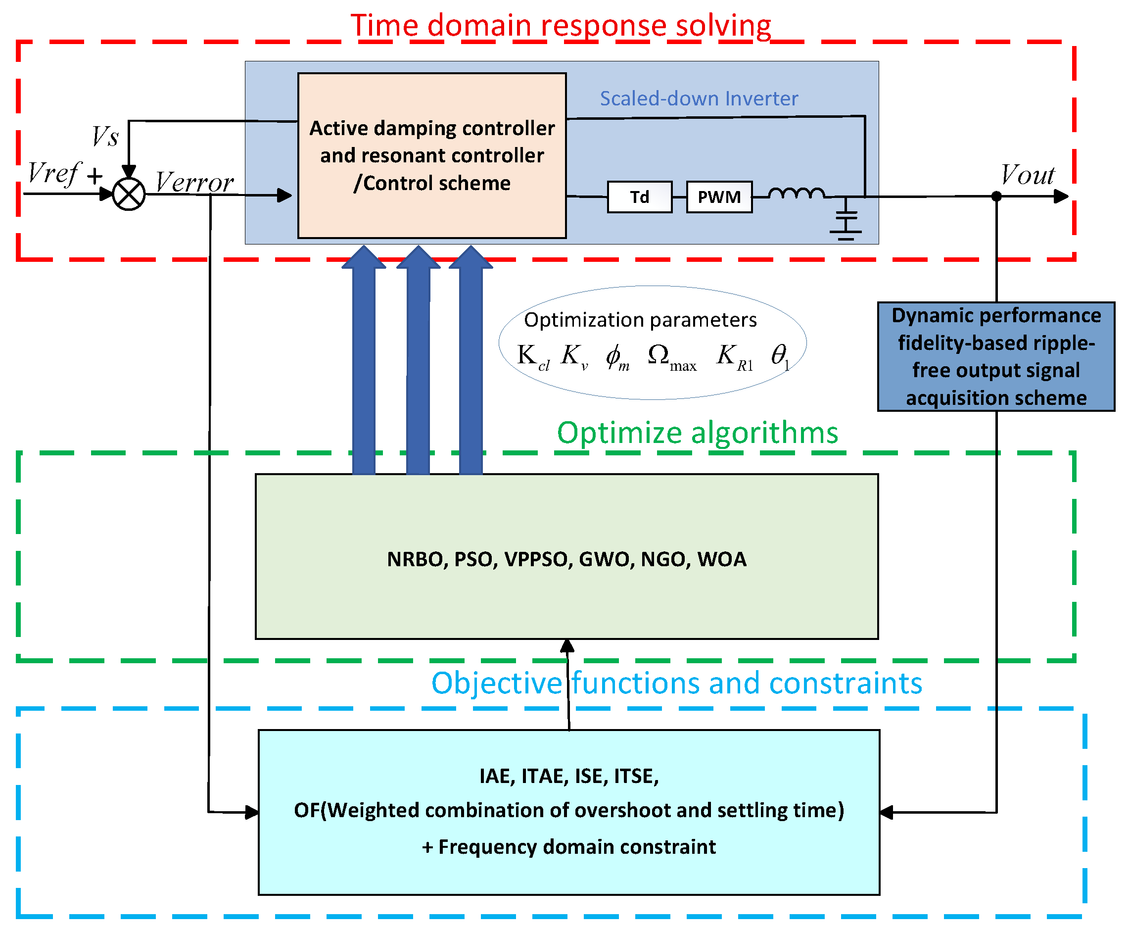
Figure 1 presents the signal flow diagram used for optimizing controller parameters in a voltage-feedback-based converter. The overall optimization framework consists of three main components: (i) time domain response solving; (ii) objective functions and constraints; and (iii) optimization algorithms. By adopting a low-latency, distortion-free control scheme together with a dynamic fidelity-based ripple-free output signal acquisition scheme, the time-domain response can be accurately and efficiently evaluated on the PHIL platform. The resulting step response indicators are then used to formulate the objective function. During each iteration, the optimization algorithm records both the objective function value and the corresponding step response indicators for the current parameter set. It then generates a new parameter combination for evaluation in the next iteration.

Figure 1.
The signal flow diagram for the controller parameter optimization of a voltage-feedback-based converter.
2.2. Objective Functions and Constraint Conditions in CDA Studies
In CDA, constructing an objective function that incorporates representative performance indicators is essential for achieving optimal performance [23]. These indicators typically include steady-state tracking error, overshoot, rise time, and settling time [1]. The optimal set of controller parameters corresponds to the condition where the objective function reaches its minimum value. Moreover, the specific formulation of the objective function should be selected based on the practical application scenario, as different performance indicators reflect different aspects of control behavior [24]. For instance, compared to absolute error-based methods, the inclusion of squared error terms imposes stricter penalties on large deviations, thereby emphasizing precise steady-state, error-free control. In recent years, various objective function design methods have been proposed to address the parameter optimization problem in multi-loop control systems of power electronic converters. Table 1 presents the mathematical expressions of typical objective functions commonly found in the literature, offering a brief overview of related studies. In Table 1, t is the simulation time, is the phase margin, is the gain margin, (or ) is the overshoot, is the rise time, is the settling time, and is the steady-state error.

Table 1.
Objective functions and references.
Online self-tuning based on the time-domain characteristics of the error signal is considered a simple and practical approach for closed-loop control [25], as the error signal is relatively easy to extract. In controller parameter optimization, several commonly used integral-based objective functions include the Integral of Absolute Error (IAE), Integral of Time-weighted Absolute Error (ITAE), Integral of Squared Error (ISE), and Integral of Time-weighted Squared Error (ITSE) [12,29]. However, a notable limitation of the IAE and ISE criteria is that they assign equal weight to all errors over time, which often results in prolonged settling times. Although the ITSE criterion mitigates this drawback by penalizing errors at later stages more heavily, it does not inherently guarantee satisfactory stability margins [28]. It should be emphasized that within this application, one of the key challenges associated with these conventional objective functions is their tendency to produce significant overshoot, which ultimately degrades overall control performance.
To address the limitations associated with integral-based objective functions, a fundamental solution lies in explicitly extracting overshoot information and incorporating it into the optimization process, either as part of the objective function or as a boundary constraint. In the study by Tang et al. [13], a chaotic ant colony algorithm was employed to optimize the FOPID controller parameters of an AVR system, where dynamic performance indices such as overshoot () and settling time () were jointly considered to construct the objective function. Gaing [27] proposed a time-domain objective function composed of classical dynamic performance metrics, including , , , and . Additionally, the function only used one weighting factor (), which meant that there was only one degree of freedom (DOF) in the optimization process. Zamani et al. [28] applied PSO to tune an FOPID controller for an AVR system. The objective function incorporated eight performance metrics, the goal was to strike a balanced trade-off between dynamic responsiveness and sufficient stability margins. However, the simultaneous inclusion of both time-domain and frequency-domain indicators, along with the need to assign appropriate weighting factors to each metric, significantly increased the complexity of achieving efficient tuning.
In this study, an objective function is proposed. The proposed function incorporates ISE, overshoot, and settling time, along with three corresponding weighting coefficients. The formulation is expressed as follows:
where – are weighting coefficients determined empirically based on multiple experimental trials, with selected values of , , and . ISE is Integral of Squared Error, represents the overshoot, and is the settling time.
Although time-domain objective function-based optimization methods can effectively improve controller performance using indicators such as overshoot and settling time, they do not directly constrain frequency-domain margins. To address this issue, the proposed study incorporates frequency-domain stability constraints into the time-domain optimization framework. This constraint condition is as shown in the equation, is Phase margin, is Phase crossover frequency. The optimization moves on to the next assessment if the stability criteria are met; if not, the objective function is given an infinite cost, and the iteration is repeated with a new candidate. This approach not only guarantees sufficient gain and phase margins for the designed controller but also reduces the search space, shortens the optimization time, and improves overall efficiency. To illustrate the efficacy of the suggested approach, a comparative analysis of five objective functions—IAE, ITAE, ISE, ITSE, and the proposed objective function (OF) will be provided in Section 5.
2.3. Modeling Methods and Time-Domain Response Solution
Since the objective function involves step response metrics, it is essential for time-domain response evaluation. The accuracy and reliability of the time-domain response depend critically on the precise modeling of delay effects within the system. However, the inherent characteristics of such delays present significant challenges to the modeling process [30]. Common methods for modeling dynamic delay effects include the state-space averaging approach and SPICE-based circuit simulation. Alternatively, time-domain responses can also be directly obtained using hardware-in-the-loop (HIL) systems with physical circuit implementation.
The fidelity-based hierarchical spectrum of delay-effect modeling techniques is illustrated in Figure 2; the power electronics modeling system can be divided into two technical paths of system-level and device-level bidirectional. The switching function approach [31] avoids the need for event handling at the system level by substituting controlled sources for physical switches; as a foundational technique in circuit averaging, the state-space averaging method has been extensively applied in modeling the behavioral characteristics of switched-mode PWM DC–DC converters, owing to its high simulation efficiency and modeling simplicity. This technique handles dynamic delay characteristics through linearization and improves simulation speed by focusing on macroscopic dynamics and neglecting switching events [32,33,34]. However, the omission of small-signal ripple modeling limits its ability to accurately capture high-frequency harmonic components in the output waveform. In device-level modeling, idealized strategies reduce model complexity by using linear equivalent components, but there exist significant discrepancies from actual physical device behavior [35]. SPICE-based circuit modeling uses basic components involving transmission lines, diodes, and capacitors to construct physical delay models [35]; it enables detailed characterization of switching transients, power losses, and thermal behavior [36]. However, the large model complexity and significant processing expense for numerical simulation are its main disadvantages.

Figure 2.
Delay effect modeling techniques with different fidelity.
As a hybrid simulation method, HIL enables real-time reconstruction of power electronic system behavior through power interfacing [37]. In this approach, a real-time simulator (RTS) emulates part of the circuit topology, while the device under test (DUT) is integrated into the system as a physical component, establishing a co-simulation framework that combines software modeling with hardware execution. The power amplifier (PA) in this configuration is essential for enabling bidirectional active power exchange and scaling signal levels. A typical power interface comprises key components such as the PA, analog-to-digital converters (ADCs), digital-to-analog converters (DACs), and various sensors. Collectively, these ensure real-time signal acquisition and energy exchange. This technology provides an efficient testing platform for analyzing the conversion characteristics, validating control strategies, and evaluating the dynamic response of power electronic systems [38]. In this study, a PHIL platform was developed using a microcontroller-based architecture.
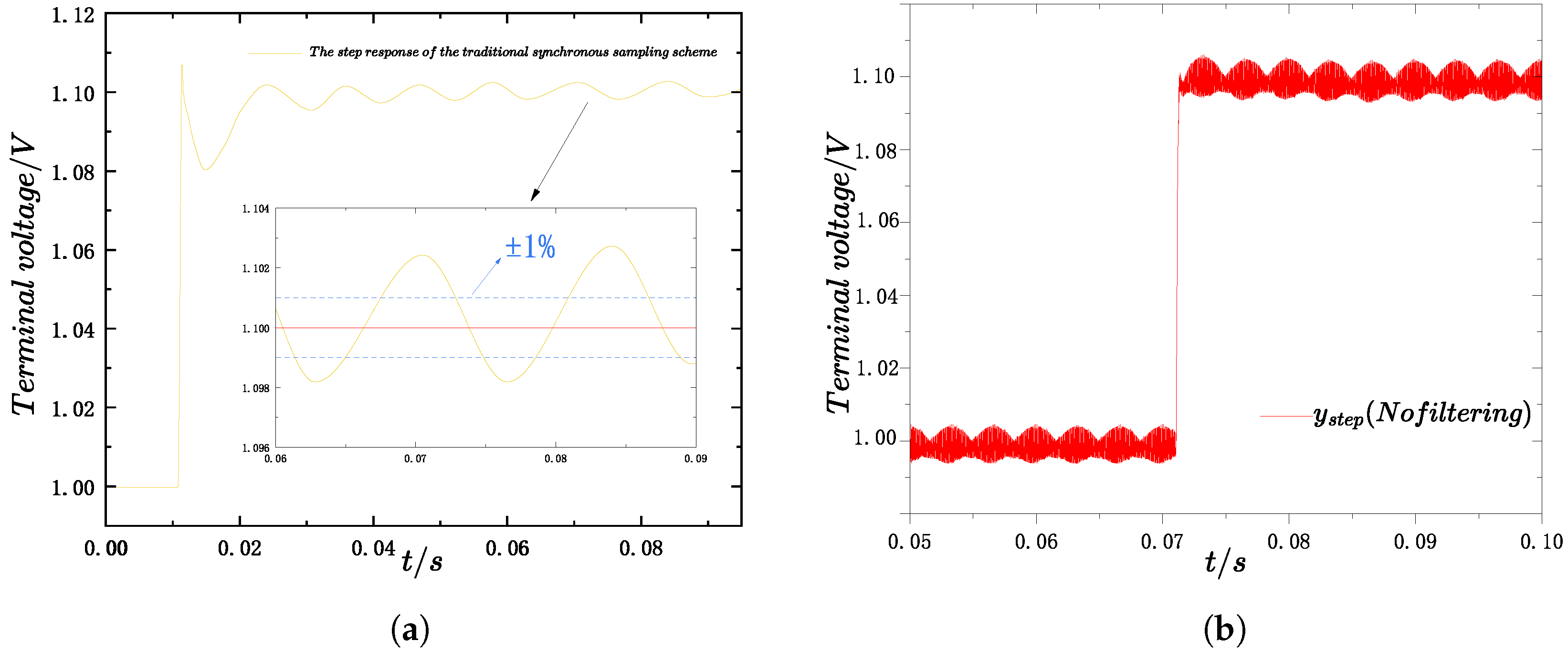
During the time-domain response solving in the PHIL framework, two critical technical challenges remain: the implementation of distortion-free and aliasing-free control, and the acquisition of a dynamic-fidelity-based, ripple-free step response signal. As illustrated in Figure 3, the comparison between the time-domain responses obtained with only filtering (still affected by aliasing) and those obtained without filtering but free from aliasing clearly demonstrates the influence of these two effects. Both factors can significantly affect the extraction of step response metrics and the effectiveness of parameter optimization. The following section presents the corresponding solutions to these challenges.
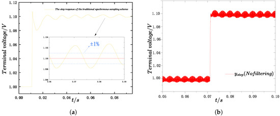
Figure 3.
Comparison of time-domain responses under different processing conditions. (a) Response obtained with filtering but affected by aliasing. (b) Aliasing-free response obtained without filtering.
3. Low-Latency, Distortion-Free Control Scheme for PHIL Time-Domain Response Solving
During the time-domain response analysis in PHIL, conventional synchronous sampling methods are prone to aliasing distortion. This distortion induces pronounced oscillations in the step response, hindering stable convergence and thereby compromising the accurate extraction of step performance indices. This paper proposes an anti-aliasing decoupled sampling voltage dual-loop active damping control topology with significantly reduced computational delay. The proposed topology integrates an inner-loop active damping mechanism based on a discrete lead compensator and an outer-loop proportional-resonant (PR) voltage controller. By employing phase-shifted synchronous sampling, the phase of sideband harmonics is adjusted to achieve harmonic cancellation. Then, the proposed parameter numerical optimization method is used to achieve the coordinated tuning of the inner and outer loop parameters.
3.1. System Modeling and Analysis
3.1.1. Topological Structure
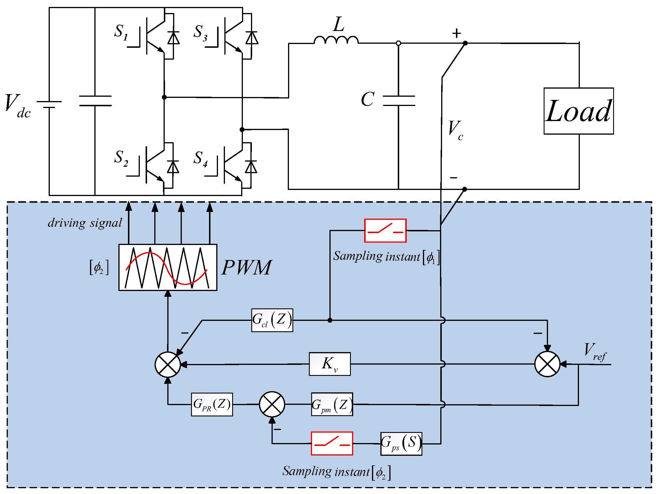
The dual-loop voltage control topology of a single-phase inverter with an LC output filter is illustrated in Figure 4. L and C represent the inductance and capacitance of the LC-type output filter, respectively, is the phase-shifting filter, is the outer-loop proportional-resonant controller, is the digital filter, is the proportional gain, the inner-loop lead compensator.
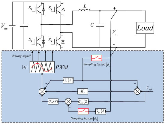
Figure 4.
System topology diagram.
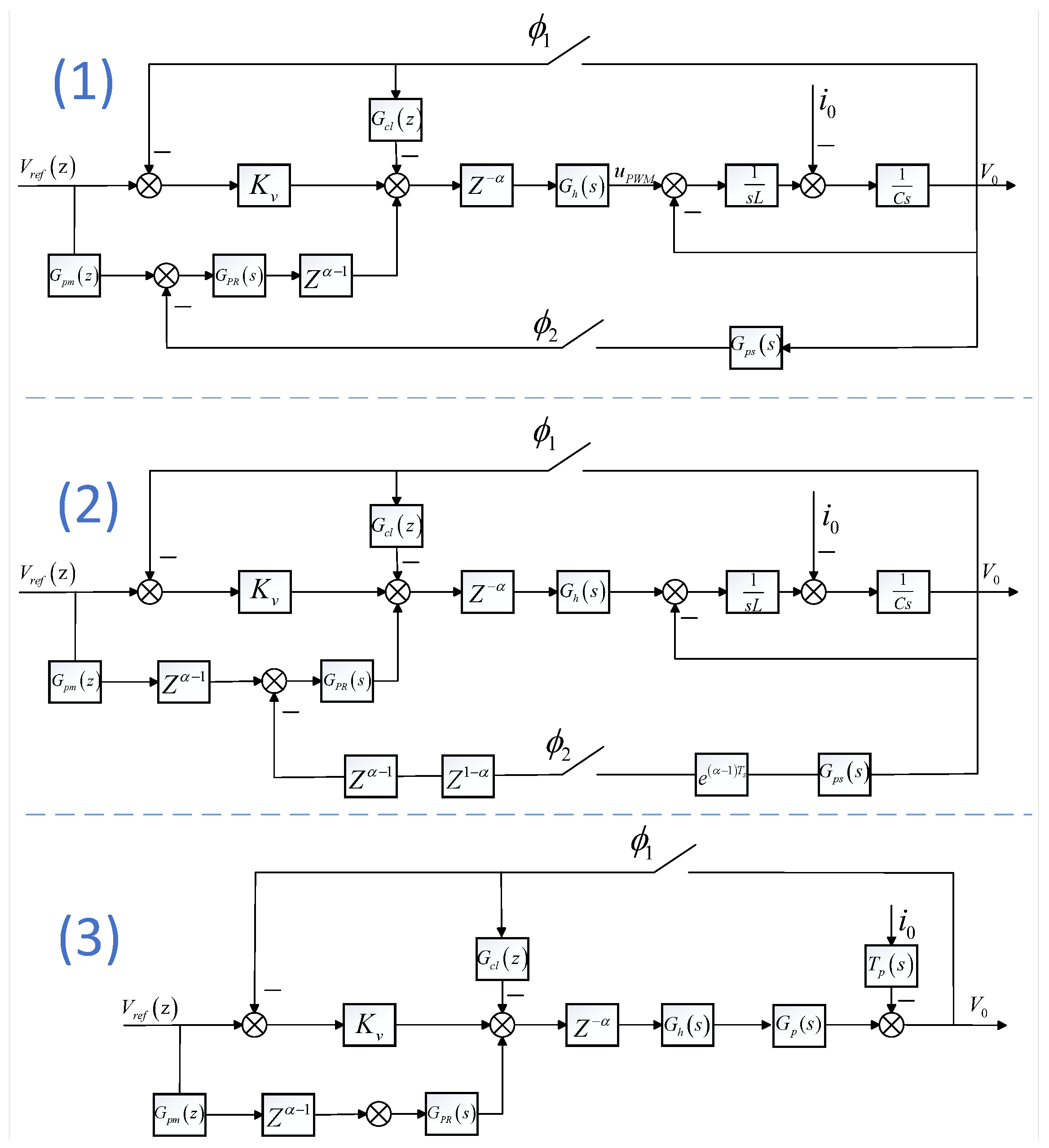
Aliasing distortion arises during the time-domain response evaluation on the PHIL testbed, which seriously affects the effectiveness of system parameter optimization. This study proposes a decoupled sampling strategy to overcome the problem. As illustrated in the inverter system shown in Figure 5, the feedback capacitor voltage signal is sampled and routed through three distinct paths. At sampling instant , the first path feeds the sampled data directly into the active damping channel, while in the second path, the reference signal is subtracted from the sampled feedback signal and then sent to the proportional channel. At sampling instant , the third path subtracts the discretized reference signal from the sampled feedback signal and sends the result to the outer-loop proportional-resonant controller. Phase-shifted synchronous sampling of the capacitor voltage feedback signal in the third path produces sampled data free of aliasing and, eventually, permits distortion-free sampling and control. The principle by which the phase-shifted synchronous sampling achieves aliasing-free performance will be elaborated in the following.
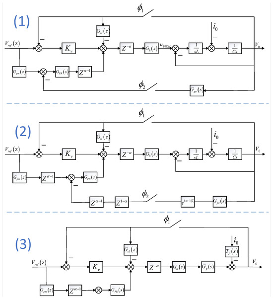
Figure 5.
Control topology: (1) original scheme; (2) discretized with modified z-transform; (3) equivalent transformed configuration.
Figure 5(1) shows the equivalent control block diagram of the control topology. As shown in Figure 5(2), the modified z-transform [39] can be used to discretize the s-domain transfer function with delay, the sampling time can be equivalent to the combined form of the sampling time with the delay [40]. To facilitate system analysis, an equivalent transformation was performed on Figure 5(2), resulting in the configuration shown in Figure 5(3).
Table 2 details the fundamental parameters of the system. The inverter is implemented as a scaled-down experimental model. The DC bus voltage is reduced to ensure laboratory safety, as the control and sampling behaviors analyzed in this study are independent of the absolute voltage level. The switching frequency of 20 kHz corresponds to widely adopted industrial operating conditions, particularly in distributed PV and energy-storage inverters. The proposed modeling and optimization methods are general and remain applicable to inverters with higher switching frequencies.

Table 2.
Main parameters of the inverter.
3.1.2. Active Damping Inner Loop Voltage Loop
The underdamped resonant poles introduced by the LC filter in the voltage loop must be effectively suppressed using damping techniques. Passive damping methods typically involve connecting damping resistors either in series or in parallel with the filter capacitor or inductor. While inherently robust, these approaches lead to significant power losses. In contrast, active damping techniques modify only the control loop and do not introduce additional power losses. Therefore, this study adopts an active damping approach, employing the discrete-time lead compensator proposed by de Souza et al. [41], with the following transfer function:
where
In the formula, is the maximum compensation phase; is the normalized discrete frequency when occurs given by (4) the relationship between and , where is the Nyquist frequency ; and is selected to obtain the maximum phase compensation. Among , , and , parameters can be obtained through value optimization to obtain the optimal solution.
3.1.3. The Design of Phase Shift Filter
The phase shift filter is implemented using a second-order active filter to cause a phase shift for signals above the switching frequency. To eliminate the phase deviation between the output and the command signal, a digital filter obtained by discretizing a first-order hold is introduced as a phase compensation module. The s-domain transfer function of a phase shift filter can be expressed as:
In this design, a switching frequency of 20 kHz is adopted. To effectively cancel high-amplitude sideband harmonics introduced during sampling, the phase shifter is required to maintain a near-ideal phase response of −90° at the 19 frequency points. The proposed design satisfies the phase and bandwidth requirements necessary for functioning as a phase shifter and meets the intended design objectives. can be designed so that the low-frequency band has almost exactly the same frequency response as , and the corresponding transfer function is given by
3.1.4. External Voltage Control Loop
Proportional Resonant (PR) control is a classical control method widely adopted in engineering applications due to its simple principle, ease of implementation, and straightforward parameter tuning. The PR controller leverages the theoretically infinite gain at the resonant frequency to effectively suppress specific harmonic components. In this study, a phase-compensated PR controller is employed. The controller is designed based on the impulse-invariant discretization method [42]. The expression is as follows:
where is the phase compensation angle, n is the order of the fundamental or harmonic component, kp is the proportional gain, while and are the resonant gains for the fundamental and the nth harmonic controllers, respectively. The compensation angle and resonant gain of the fundamental resonant controller can be determined through numerical optimization. In addition, the outer-loop proportional controller is denoted by , and its optimal value can also be obtained using numerical parameter optimization. Accordingly, the outer-loop voltage controller in the Z-domain is given by:
The modeling of sampled discrete-time sequences in conjunction with the digital pulse-width modulation (DPWM) system can be accomplished using a normalized zero-order hold (ZOH). The ZOH transfer function in the s-domain is given by:
The controlled plant can be described by the following equation:
By substituting the complex variables and , the system’s frequency response characteristics can be analyzed in the continuous-discrete hybrid domain. The inner and outer control loops have the following open-loop transfer functions:
The inner and outer control loops have the following closed-loop transfer functions:
3.2. The Principle of Eliminating Aliasing by Synchronous Sampling of the Moving Phase
In this study, a unipolar multi-frequency sinusoidal pulse width modulation (SPWM) digitally controlled single-phase inverter is utilized. The harmonics of the output voltage can be represented as follows [43]:
The harmonic of the inverter output voltage is expressed as , M is the modulation ratio, is the carrier angular frequency and its frequency is equal to the switching frequency, is the modulation wave angular frequency, m and n are the multipliers of the carrier and modulation wave, respectively. is the carrier phase angle; is the modulation wave phase angle. The distribution characteristics of the PWM sideband harmonic spectrum after the action of can be expressed as [43]:
where , is the fundamental angular frequency, and is the carrier angular frequency. After sampling at the angular frequency of , according to the aliasing law [44], it can be expressed as:
where is a sampling instance within the carrier period. When the pulse ratio is high, q = m. Therefore, the component on the harmonic reference can be expressed as:
Obviously, when and , . Therefore, if the phase of the LC filter is maintained at or beyond the carrier phase, the sideband harmonics can be completely canceled after sampling, achieving alias-free sampling. Alternatively, alias-free sampling can also be realized by applying a phase shift to the PWM signal using an analog phase-shifting filter before sampling, combined with synchronous sampling.
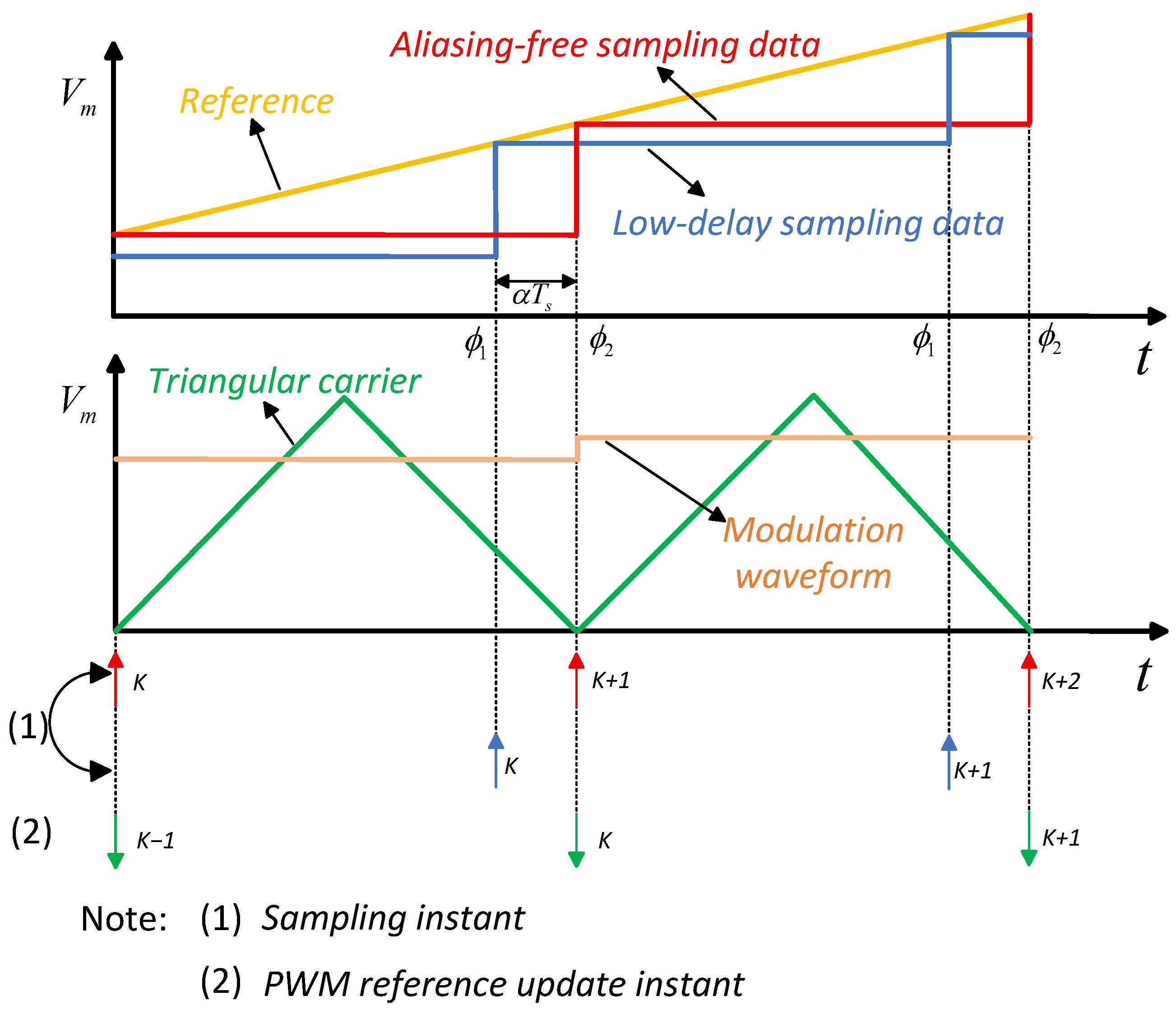
The arrangement of updating and sampling instants is illustrated in Figure 6. To reduce delay, is positioned as near as possible to the duty cycle update moment, so that only the computation time for the duty cycle remains instead of an entire beat. The phase ensures alias-free sampling. represents the computation time ratio, defined as the computation time divided by the sampling period. In synchronous sampling mode, the output voltage of the inverter is sampled during the kth sampling period, and after being processed by the digital signal processor through the control algorithm, the resulting control signal is not transmitted to the digital pulse width modulation (DPWM) stage until the beginning of the (k + 1) th period.

Figure 6.
Sampling and update instants in the digital PWM.
To facilitate a fair comparison between the phase shifter and the anti-aliasing filter, a second-order low-pass filter with identical poles to the phase shifter was employed. As illustrated in Figure 7, the low-pass filter achieves lower overall aliasing in certain phase conditions but its minima fluctuates with the modulation index M, and it is difficult to maintain consistently low aliasing levels when the reference voltage amplitude varies. In contrast, the proposed phase-shifted sampling method maintains the lowest aliasing levels for all harmonics under synchronous sampling, confirming its advantage over second-order low-pass filtering in suppressing aliasing.

Figure 7.
Theoretical aliasing amplitudes of the carrier frequency normalized at different sampling instants.
3.3. The Construction of a PHIL Experimental Platform and Validation of the Proposed Aliasing Distortion Model
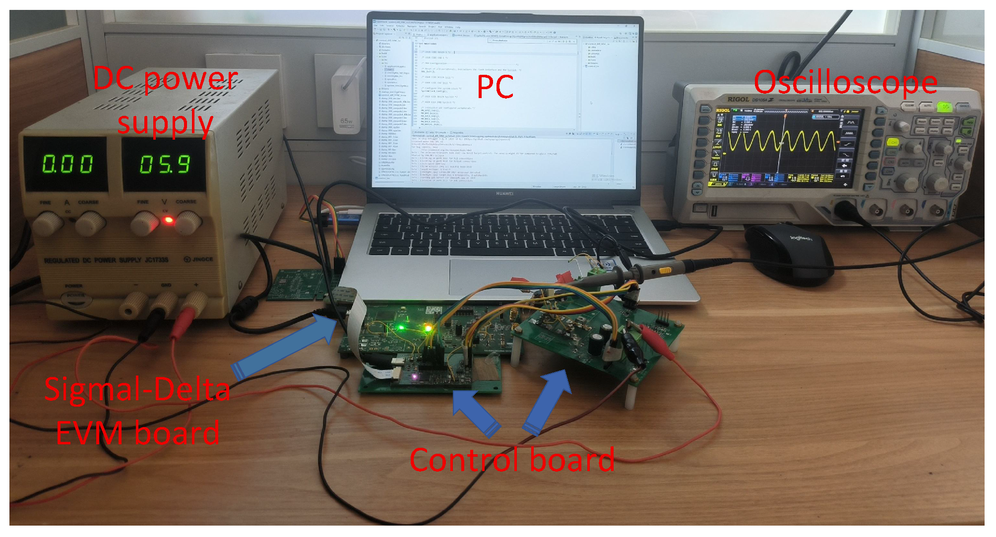
As illustrated in Figure 8, an entire PHIL experimental platform was developed to validate the proposed controller design and optimization approach. A Sigma-Delta evaluation board (ADS127L01, Texas Instruments, Dallas, TX, USA) is positioned at the bottom to acquire voltage data and calculate the total harmonic distortion (THD). A stable DC voltage source is on the left. For measurement purposes, the system incorporates an oscilloscope paired with voltage probes to capture real-time data on capacitor voltage. In addition, the digital controller outputs an analog error signal via its DAC to facilitate waveform observation through the oscilloscope. In the experimental setup, the STM32G474CEU6 microcontroller (STMicroelectronics, Geneva, Switzerland) was selected to perform the control functions. To achieve high-precision signal acquisition, an external ADC (ADS8865, Texas Instruments, Dallas, TX, USA) was employed. This converter allows precise control over the sampling window via timing signals and offers a high spurious-free dynamic range (SFDR) of up to 112 dB, which enables accurate detection of low-magnitude harmonic components. Compared to the integrated ADC, it provides significantly lower nonlinear distortion. Consequently, the external ADC was designated for critical sampling instances requiring high fidelity, while the internal ADC was used for auxiliary sampling instances . Although the internal ADC of the STM32 offers a higher nominal sampling rate, its linearity, jitter performance, and harmonic fidelity are insufficient for detecting low-amplitude sideband components. Therefore, ADS8865 is employed for the critical sampling instant . Its 1.2 s acquisition time occupies only 2.4% of the 50 s control period, introducing no delay in the real-time control loop. The internal ADC is used only for auxiliary sampling , forming a hybrid sampling architecture that ensures both high fidelity and real-time feasibility. Both the voltage signal and the error signal are output from the microcontroller buffer. Furthermore, optimization algorithms are executed directly on a host PC. The system records controller parameters, objective function values, and step response data during each iteration, thus supporting a fully automated and closed-loop controller parameter tuning process.
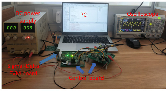
Figure 8.
The scaled-down PHIL experimental platform.
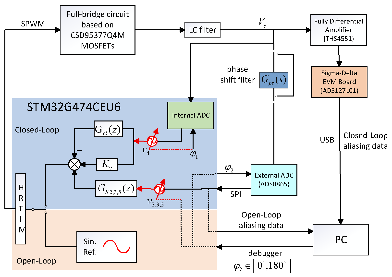
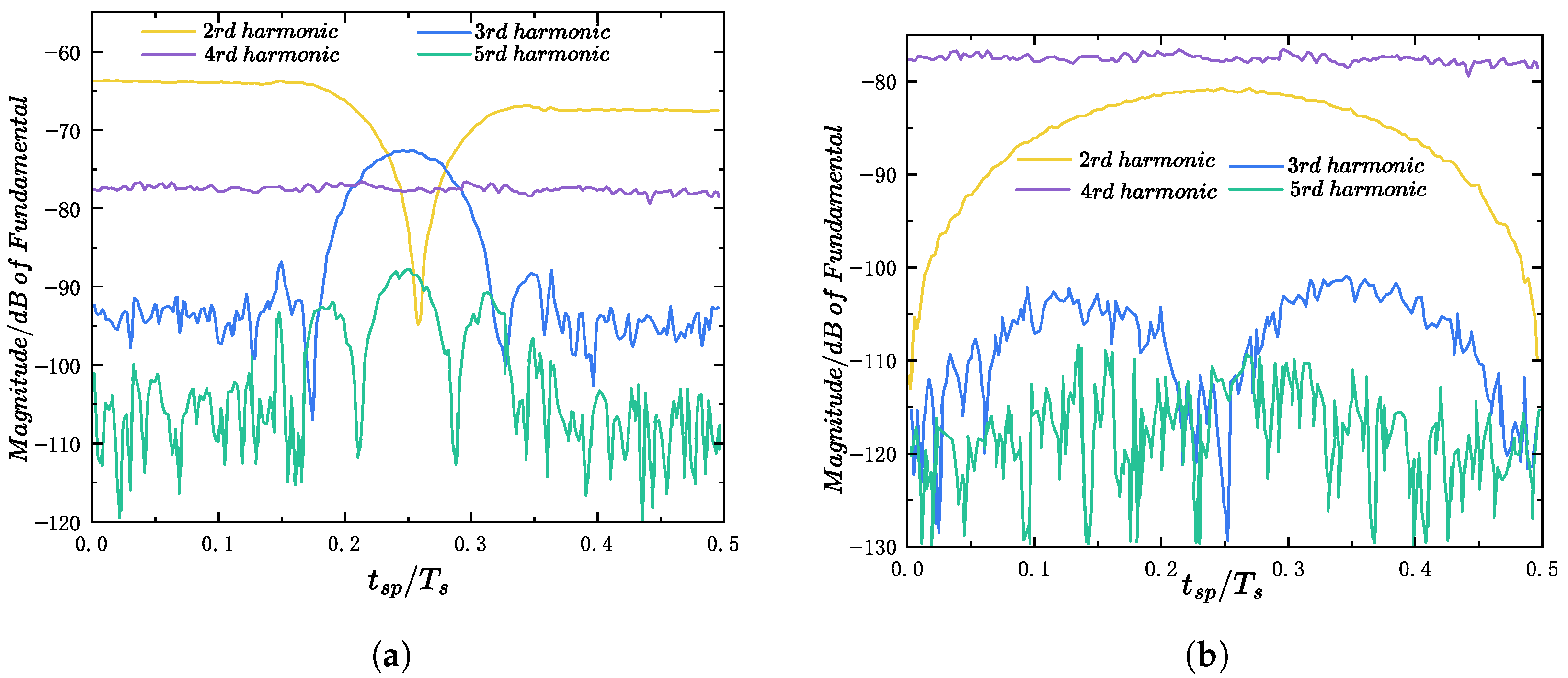
To evaluate the applicability of the aliasing distortion model under closed-loop control, experiments were conducted at a modulation index of . The configuration of the experimental system is shown in Figure 9, where the output voltage was sampled using an external high-resolution ADC. The low-order harmonic amplitudes were extracted under varying sampling phases to compare the results before and after introducing a phase shifter. Figure 10 illustrates the variation of harmonic amplitudes with respect to the sampling phase, without and with a phase shifter, respectively. Although the external ADC has limited resolution, resulting in a certain level of background white noise at higher frequencies, the trends of the second- and third-order harmonics remain clearly observable. Furthermore, since no fourth-order resonant controller was implemented in the system, the amplitude of the fourth-order harmonic in Figure 10 remains unaffected by the sampling phase, which is consistent with expectations. In Figure 10b, the low-order harmonics introduced by DPWM are effectively suppressed by the corresponding resonant controller. The remaining dominant component arises from aliasing distortion, which reappears with a trend consistent with that approximated in Figure 7b. As shown in Figure 10, the closed-loop scheme with the phase shifter yields significantly suppressed low-order harmonics, which verifies the effectiveness of the proposed aliasing-free control scheme.
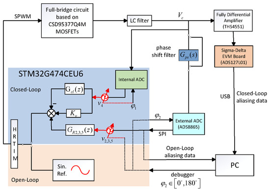
Figure 9.
The configuration of the experimental system.
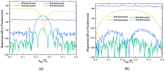
Figure 10.
Low-order harmonic amplitudes at different sampling instants under closed-loop conditions. (a) Without Phase Shifter. (b) With Phase Shifter.
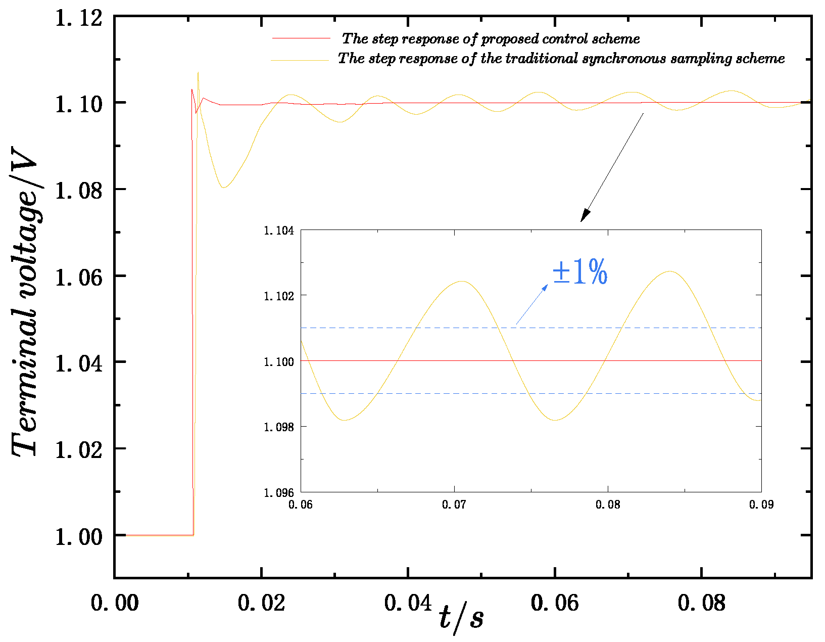
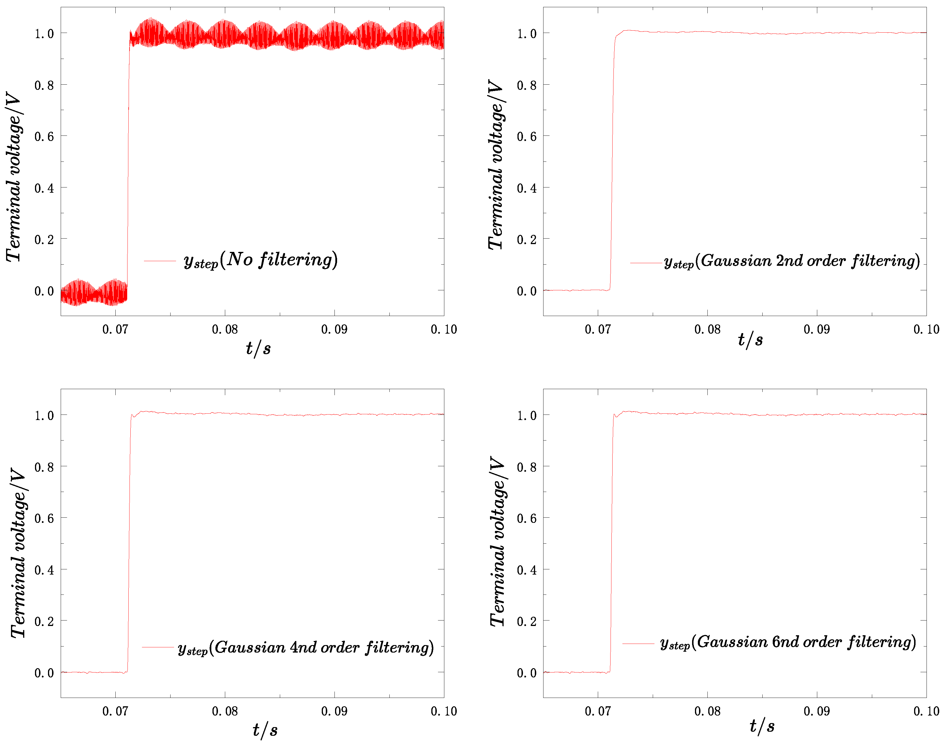
As shown in Figure 11, compared with the conventional synchronous sampling scheme that suffers from aliasing distortion, the proposed control scheme enables alias-free sampling and control, so that the step response reaches a steady state without oscillations, thereby facilitating the accurate extraction of step performance indices. It is worth noting that Figure 11 shows the result after filtering; otherwise, there would be significant ripples in the step response. The filtering method will be discussed in the next section.
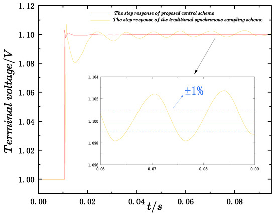
Figure 11.
Comparison of the step response quality between the proposed control scheme and the synchronous sampling scheme.
4. Dynamic Fidelity-Based Ripple-Free Output Signal Acquisition Scheme
When the resonance frequency of the LC filter is relatively high, the ripple amplitude in the system’s output signal increases significantly. As a result, the step response curve obtained through synchronous rotating frame transformation exhibits significant ripple, making it difficult to accurately extract key performance indicators such as overshoot and settling time. It will affect the construction of the objective function of the parameter optimization algorithm and reduce the effectiveness of parameter optimization. To address this issue, a ripple-free output signal acquisition scheme must be designed to meet the following constraints. There is no aliasing distortion in the feedback signal, thorough suppression of ripple, and the dynamic characteristics are faithfully preserved.
In the field of signal processing, filters are generally categorized as analog or digital. Analog filters operate directly on continuous-time signals, whereas digital filters require the input signal to be converted into digital format using an analog-to-digital converter (ADC) prior to processing. After digital filtering, the signal is typically converted back to analog form via a digital-to-analog converter (DAC) [45]. To avoid aliasing distortion in digital filtering, oversampling is required before filtering. In this study, an 8× oversampling rate is adopted to ensure alias-free signal acquisition. Additionally, selecting a sampling phase with reduced harmonic components further enhances the filtering performance. For analog filtering, downsampling must be performed after filtering to ensure complete suppression of ripple. Similarly, an appropriate sampling phase with low harmonic content is selected to optimize the filtering effect. Through these measures, both digital and analog filtering approaches are capable of generating a ripple-free and distortion-free step reference waveform, which serves as a reliable foundation for subsequent controller parameter optimization.
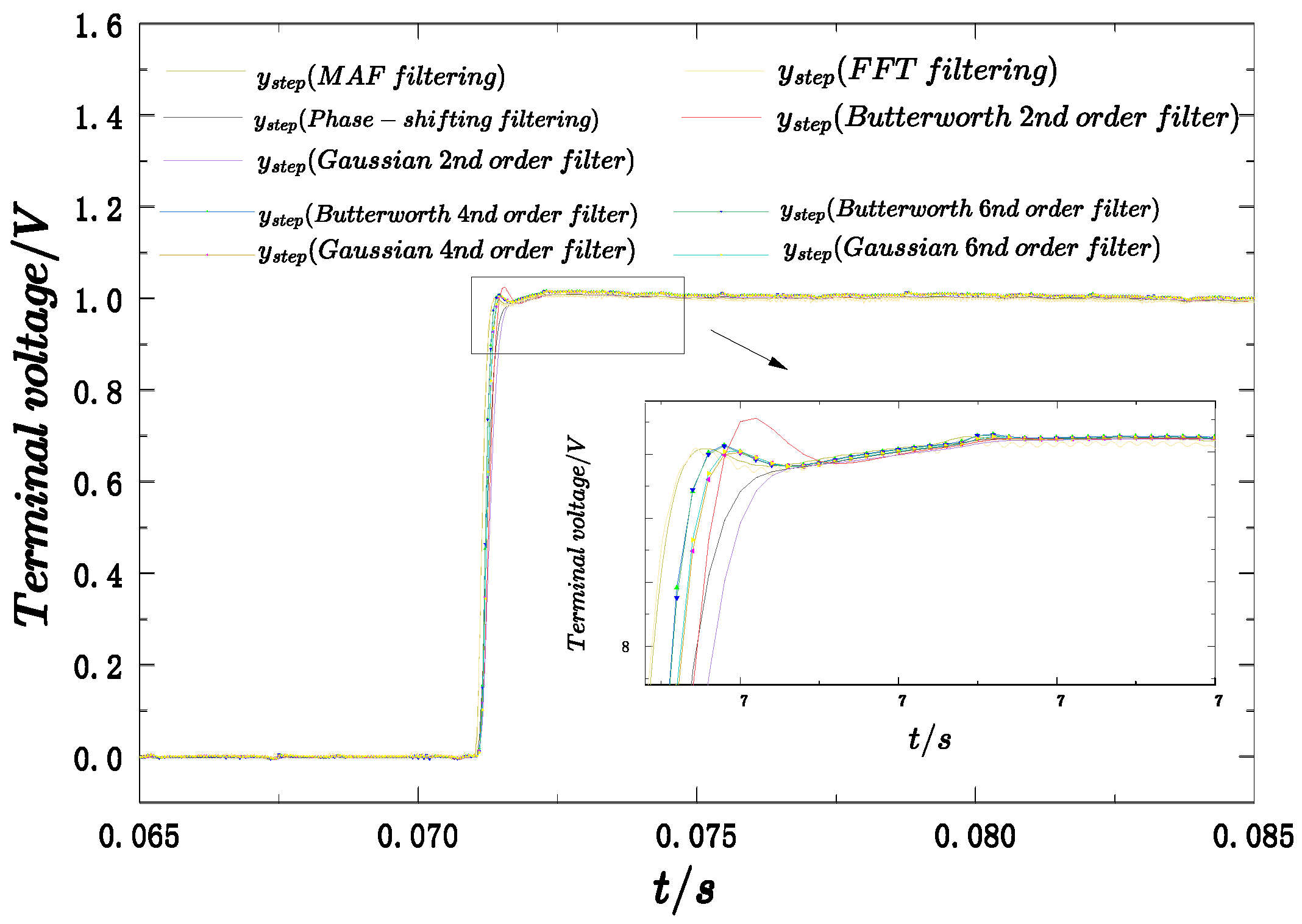
In this study, three digital filtering methods and two analog filters were selected and designed to suppress ripple. The digital filtering approaches include time-domain moving average filtering, frequency-domain windowed FFT filtering, and the phase-shifting synchronous sampling technique proposed in the previous text. For analog filtering, Butterworth and Gaussian filters were designed based on attenuation characteristics of the sideband signal of the moving average filter. Then, by comparing the ripple suppression capability, cost, and dynamic response characteristics, the filter method with the best overall performance is ultimately selected as the final ripple filtering solution.
The FFT analysis is performed using 8000 sampling points within a 0–0.01 s acquisition window. An oversampling factor of 8× or 16× is applied for the moving-average and other digital filtering methods. It should be noted that FFT-based filtering is used solely as an offline benchmark for evaluating dynamic-response fidelity and is not intended for online implementation. Other digital filtering approaches are compared against the FFT results to identify which method best approximates the high-fidelity step response while remaining suitable for real-time application.
4.1. Moving Average Digital Filtering
The moving average filtering method is a widely used digital signal processing technique in data analysis. Its core principle is to replace each sample with the average of multiple samples within a defined window, thereby reducing the influence of random noise or high-frequency components on the signal. The mathematical expression of the moving average filter is given by:
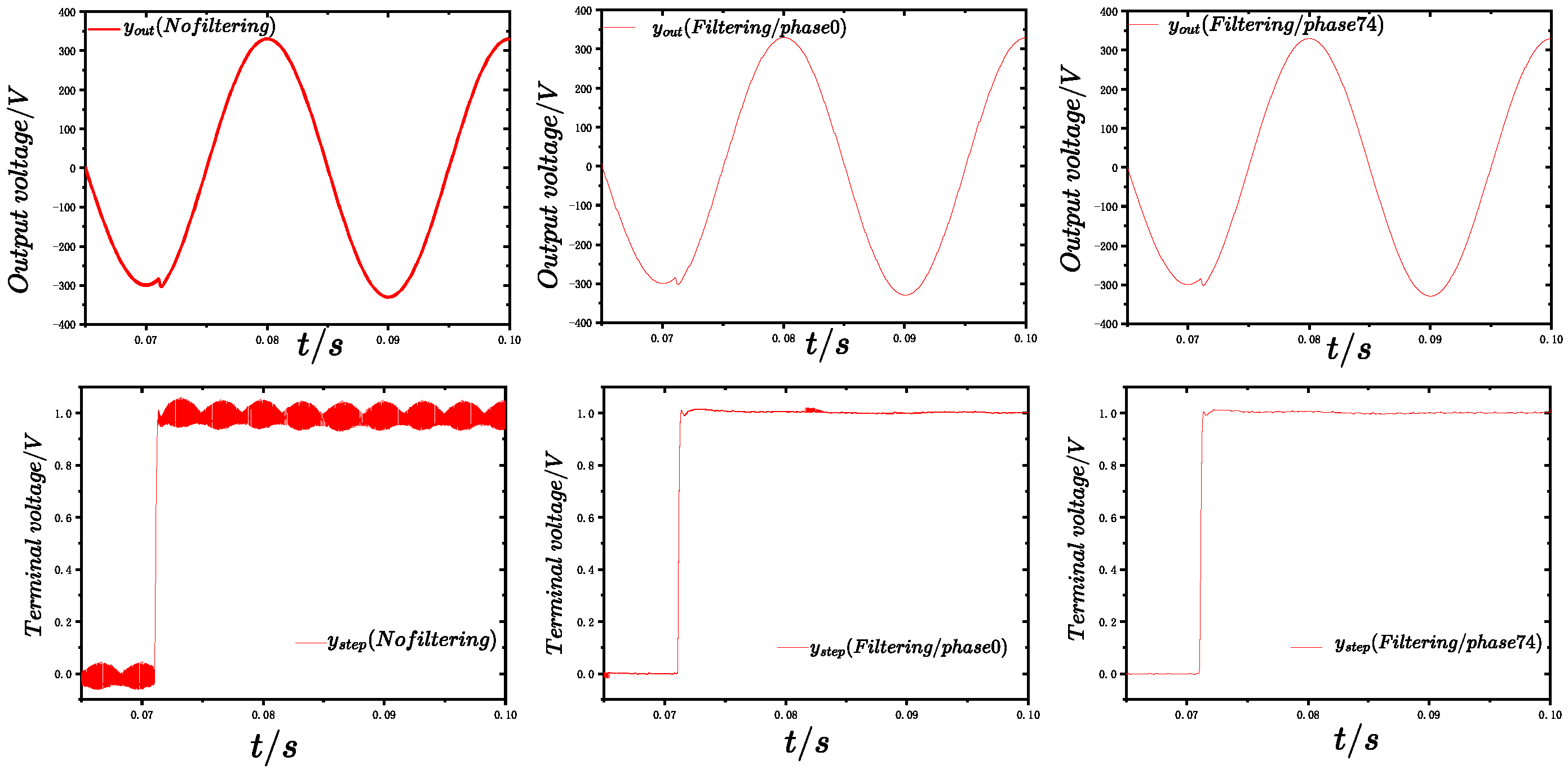
where is the filtered output value, is the current sample of the input signal, N is the window size, and k denotes the position index of the current window. The moving average filter (MAF) achieves varying degrees of noise reduction while preserving the overall signal trend by adjusting the window size. It features a simple algorithmic structure and high computational efficiency. In this study, an 8× oversampling rate is employed; accordingly, the sliding window size is set to 8. Furthermore, when the sampling phase is set to , the amplitudes of the harmonic components are significantly reduced. As shown in Figure 12, the upper group of three curves represents the output signals under three different conditions: without filtering, with MAF filtering at a sampling phase of , and with MAF filtering at a sampling phase of .
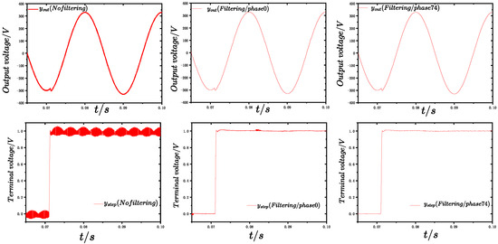
Figure 12.
Moving average filtering effect.
4.2. FFT Digital Filtering
FFT digital filtering is a frequency-domain filtering technique that involves transforming the signal from the time domain to the frequency domain, applying filtering based on a specified cutoff frequency, and then converting the signal back to the time domain. This approach enables efficient signal filtering through frequency-domain operations and is widely used in the field of signal processing.
As illustrated in Figure 13, the system exhibits a smooth and distortion-free step response in the middle of the period, whereas distortions are evident at the initial and final stages.

Figure 13.
FFT filtering effect.
4.3. Phase-Shift Synchronous Sampling Digital Filtering
Based on the previous discussions, an effective and straightforward approach to achieve aliasing-free and distortion-free ripple suppression is to apply a phase-shifting filter before sampling, which introduces a phase shift of to the sideband harmonic components, followed by synchronous sampling. This method ensures distortion-free low-frequency components and suppresses the introduction of high-frequency ripple. The detailed formulas and underlying principles were introduced earlier. As illustrated in Figure 14, the proposed method yields a distortion-free step response in the system.
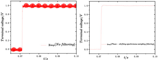
Figure 14.
Phase-shifting synchronous sampling filtering effect.
4.4. Butterworth and Gaussian Analog Filtering
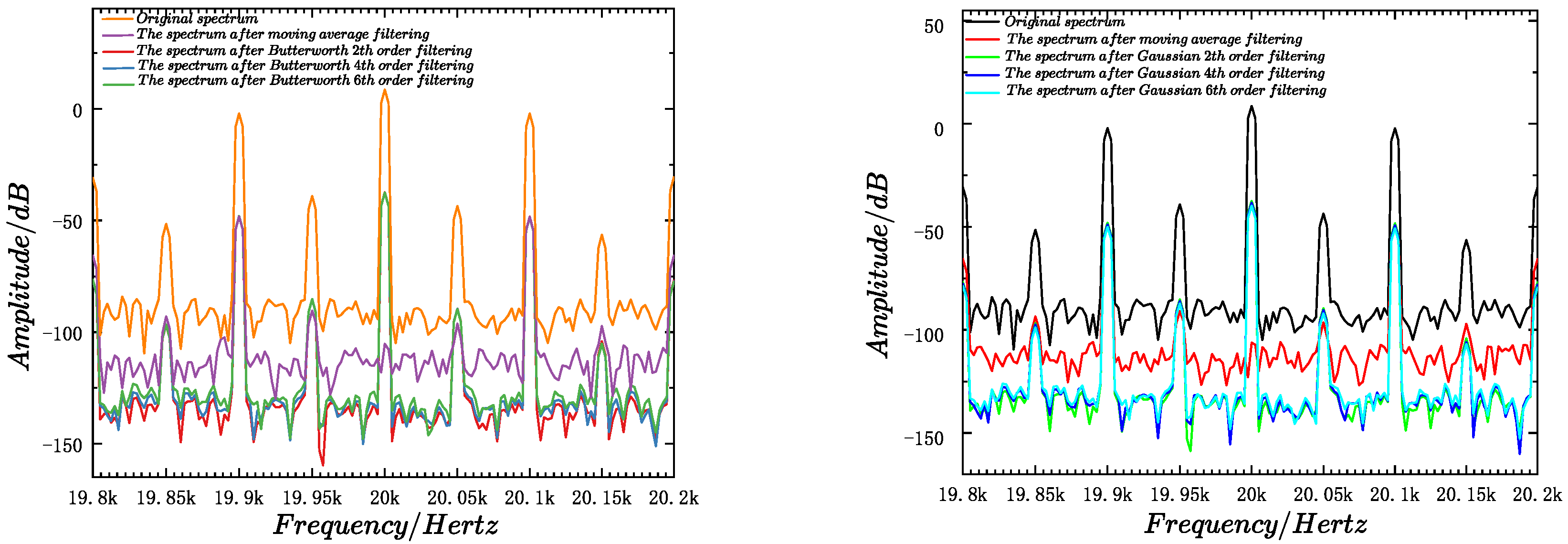
The voltage feedback system in the designed LC grid-forming inverter operates with both the switching frequency and the sampling frequency set to 20 kHz. The step signal is obtained by transforming the three-phase output voltages into the synchronous rotating reference frame (dq transformation). The dq-frame step response is obtained after filtering, where filtering has effectively removed the switching-frequency components and harmonics. Therefore, these components have negligible effect on the dq-frame step response. However, the presence of sideband components significantly affects signal acquisition quality. To address this, analog filters can be designed to match the sideband attenuation capability of the moving average filter. Specifically, the moving average filter attenuates the second-order harmonic at 19.95 kHz from dB to dB, and the third-order harmonic at 19.90 kHz from dB to dB. Based on this sideband suppression profile, Butterworth and Gaussian analog filters were designed accordingly. The sideband attenuation performance near 20 kHz for the moving average filter and the designed analog filters is shown in Figure 15.
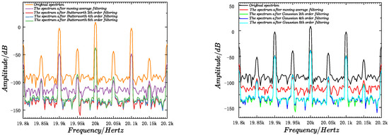
Figure 15.
Design principles of different analog filters. Left: The design basis of the Butterworth filter. Right: The design basis of the Gaussian filter.
The Butterworth filter is a classical Infinite Impulse Response (IIR) filter commonly used in applications where ripple in the passband and stopband is unacceptable. Its primary advantage lies in its maximally flat magnitude response across all frequency ranges, characterized by a gain of unity in the passband and zero in the stopband. It has a roll-off of −20 dB per decade per pole, and its phase response becomes more nonlinear as the filter order rises [46]. The transfer function corresponding to the Butterworth filter is defined as [45]:
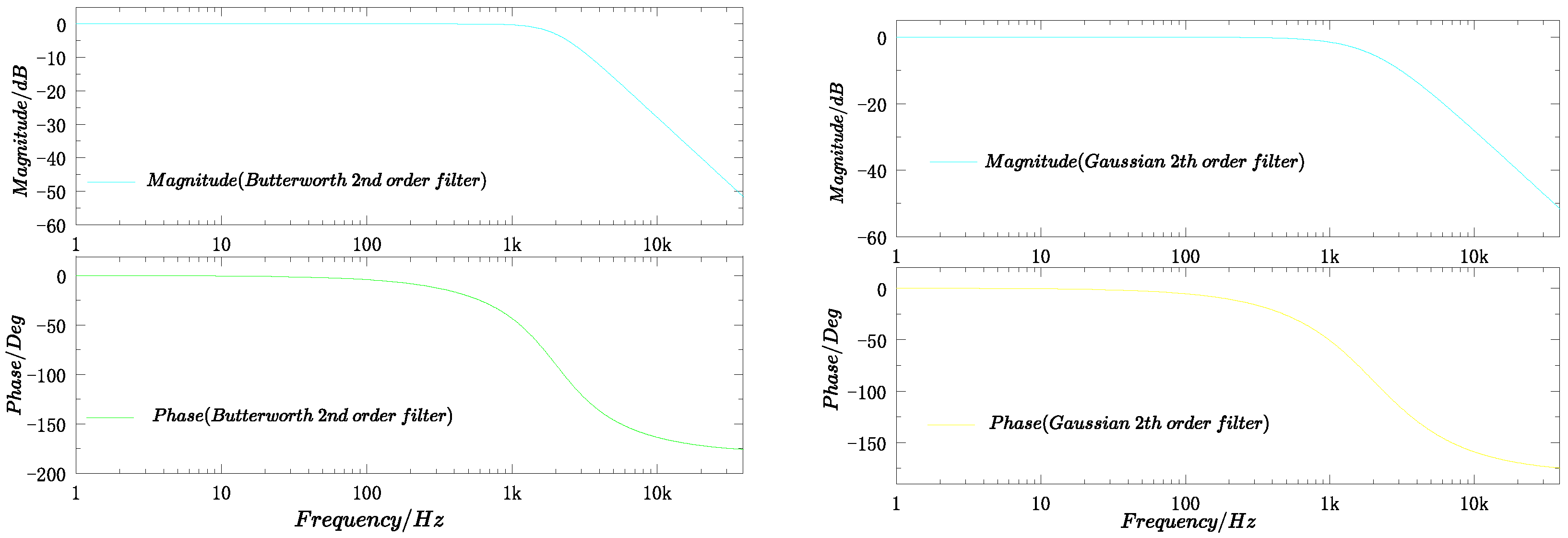
where n is the order of the filter. The Gaussian analog filter, based on the Gaussian function, is characterized by a smooth transition band in the frequency domain and a time-domain response free from ringing effects. In this study, both Butterworth and Gaussian low-pass analog filters were designed with three different orders: 2nd, 4th, and 6th. Figure 16 provides the amplitude and phase response curves for the implemented Butterworth and Gaussian filters.
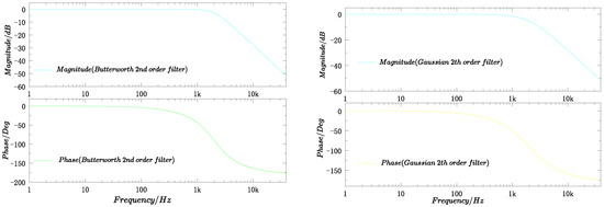
Figure 16.
Comparison of amplitude–frequency characteristics of two analog filters. Left: Frequency characteristics of Butterworth 2nd-order filter. Right: Frequency characteristics of Gaussian 2nd-order filter.
Given that the sampling frequency is 20 kHz, the decimation rate after analog filtering is also configured to 20 kHz. Furthermore, setting the sampling phase to significantly attenuates the harmonic content in the system. As shown in Figure 17, Figure 18 and Figure 19, this results in a ripple-free step response.
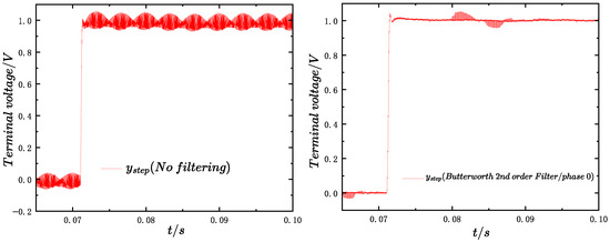
Figure 17.
Butterworth 2nd-order filtering effect (phase 0).

Figure 18.
Butterworth filtering effect (phase 44).
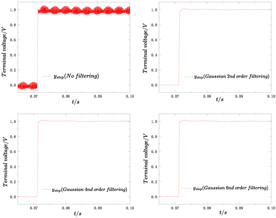
Figure 19.
Gaussian filtering effect.
4.5. Comparison of Filtering Effects
Figure 20 compares the filtering performance of five methods applied to the voltage-feedback system. Since FFT–IFFT processing introduces inherent delays and boundary distortions, it is used solely as an offline benchmark, rather than as an option for online filtering. The other digital filtering methods are assessed based on how closely their dynamic responses approximate this high-fidelity FFT benchmark while remaining feasible for real-time implementation. After comprehensive comparison, the MAF method is selected as the ripple-suppression scheme because it achieves dynamics closest to the FFT benchmark, avoids boundary distortions, and offers good cost-performance, simplicity, and practicality. This enables accurate extraction of step-response metrics for objective-function construction and supports subsequent controller-parameter optimization.
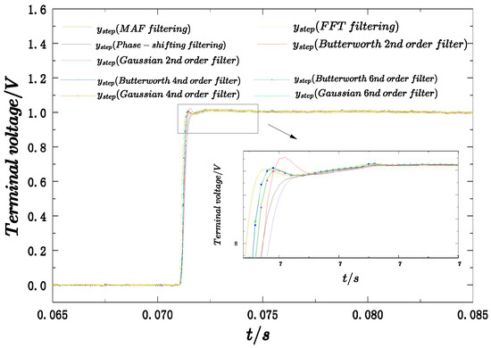
Figure 20.
Comparison of all filtering effects.
5. Parameter Optimization Experiment
5.1. Overall Experimental Scheme Overview
Artificial intelligence (AI) has been widely applied in the design of power electronic systems [47]. Among various AI-based techniques, meta-heuristic algorithms have emerged as powerful tools for control parameter optimization due to their efficient global search capability [48]. However, nature-inspired meta-heuristic algorithms possess inherent drawbacks. Their reliance on local search strategies and random initialization often leads to premature convergence toward local optima [49], while their stochastic nature can cause significant variations between runs [50]. To overcome these limitations, hybrid optimization strategies that integrate multiple meta-heuristic algorithms have attracted increasing attention. By leveraging the complementary strengths of different algorithms for parameter optimization and selecting the best-performing solution through comparative evaluation, such hybrid approaches can effectively mitigate local optimality issues and enhance the reliability of optimization results.
In this study, six optimization algorithms are employed: Newton–Raphson-Based Optimization (NRBO), particle swarm optimization (PSO), Velocity-Partitioned Particle Swarm Optimization (VPPSO), gray wolf optimization (GWO), Northern Goshawk Optimization (NGO), and Whale Optimization Algorithm (WOA). During each iteration, the selected algorithm evaluates control performance by invoking a designated objective function—IAE, ITAE, ISE, ITSE, or the proposed objective function (OF). The corresponding objective value and the time-domain response are recorded, and a new parameter candidate is subsequently generated for the next control evaluation. After completing the specified number of iterations, the best-performing parameter set (i.e., the one yielding the minimum objective function value) is identified for each algorithm. The final optimal controller parameters are then determined by comparing the performance metrics associated with all six candidate solutions. The initial parameter configurations of the six metaheuristic algorithms are shown in the following Table 3.

Table 3.
Initial parameter configurations of the meta-heuristic algorithms.
5.2. Experimental Results and Analysis
Table 4, Table 5, Table 6, Table 7 and Table 8 present the results of the controller parameter optimization obtained from 30 independent PHIL-based optimization experiments. The data in the table present the results of full combination parameter optimization experiments conducted between six optimization algorithms (NRBO, PSO, VPPSO, GWO, NGO, WOA) and five objective functions (IAE, ITAE, ISE, ITSE, OF).

Table 4.
Parameter optimization results of different algorithms with the objective function of IAE.

Table 5.
Parameter optimization results of different algorithms with the objective function of ISE.

Table 6.
Parameter optimization results of different algorithms with the objective function of ITAE.

Table 7.
Parameter optimization results of different algorithms with the objective function of ITSE.

Table 8.
Parameter optimization results of different algorithms with the objective function of OF.
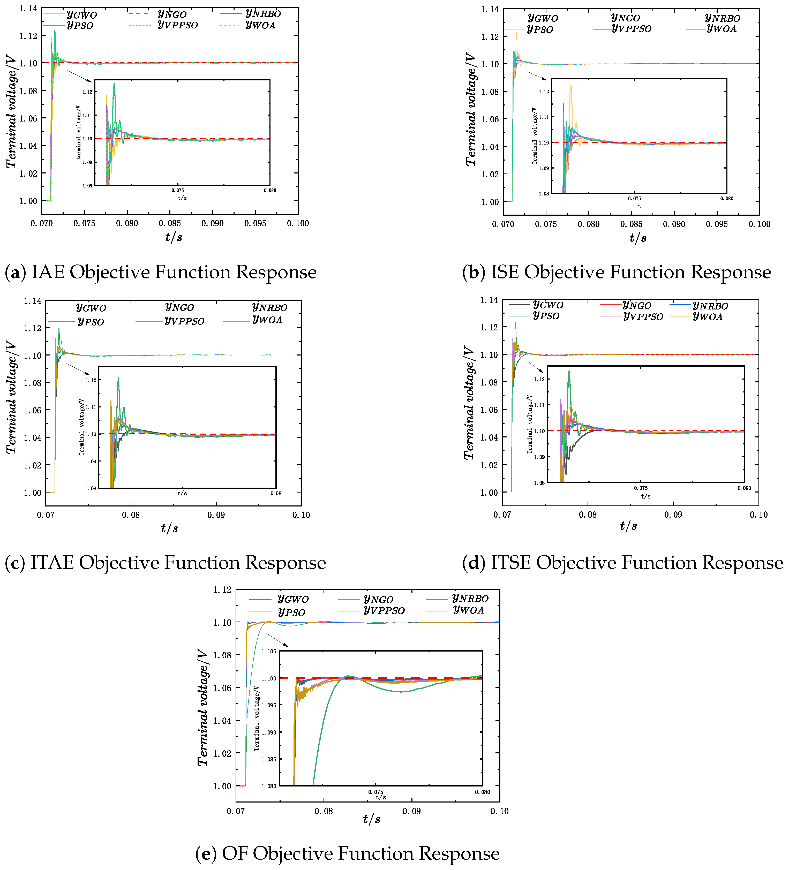
Table 9 quantitatively analyzes the control performance indicators of each test, specifically including overshoot and settling time. Additionally, the step response curves of five objective functions (IAE, ITAE, ISE, ITSE, OF) were visually compared under the PHIL experimental conditions, and the relevant results are presented in Figure 21.

Table 9.
Experiment response for different optimization algorithms.
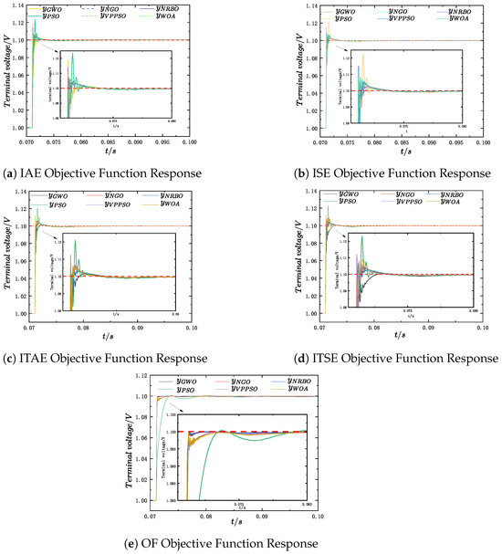
Figure 21.
Step responses under different objective functions.
Under the IAE objective function, WOA delivers the best overall performance, achieving the smallest overshoot and the shortest settling time among all algorithms. When optimizing for ISE, GWO achieves the lowest overshoot with a moderate settling time, while both VPPSO and WOA yield the shortest settling times, with WOA maintaining a smaller overshoot than VPPSO. In the case of ITAE, NGO demonstrates superior performance, with the lowest overshoot and a reasonable settling time. For the ITSE objective function, GWO again provides the lowest overshoot; however, its settling time is comparatively longer. Meanwhile, NRBO presents a more balanced behavior, combining moderate overshoot and settling time, making it the most favorable algorithm under this objective. When optimized using the proposed OF, NGO attains the smallest settling time and a moderate overshoot.
Table 10 provides a comparative analysis of the optimal step response characteristics and transient performance parameters achieved by each objective function. Experimental results demonstrate that controllers optimized with the proposed objective function have significantly better step response quality than those based on traditional objective functions.

Table 10.
Comparison of step responses of optimal results for different objective functions.
6. Conclusions
The adoption of a PHIL testbed greatly accelerates the CDA process for the voltage feedback grid-forming inverters. To address the issue of severe overshoot associated with conventional integral-based approaches, an objective function incorporating step response metrics was employed. To overcome the conflicting demands of accuracy, computational efficiency, and modeling cost in simulation-based methods, scaled-down inverter hardware was developed for time-domain response solving. To overcome the low-frequency distortion caused by conventional synchronous sampling in PWM inverters, the study analyzed the sideband aliasing regularity of capacitor voltage sampling and the mechanism of harmonic cancellation. Aliasing-free sampling is achieved via 90° phase-shifted anti-aliasing filters in conjunction with synchronous sampling, which exhibits first-order attenuation and reduces aliasing distortion more effectively than second-order filters. To filter out the ripple components superimposed on the step response, four acquisition filtering schemes were compared with FFT filtering, which offers the highest dynamic fidelity but exhibits severe distortions near the window boundaries. Oversampling combined with the MAF achieves dynamics closest to the FFT benchmark while avoiding boundary distortions. The proposed distortion-free control scheme and dynamic fidelity-based ripple-free output signal acquisition scheme enable accurate and efficient time-domain response evaluation on the PHIL testbed, providing a reliable basis for controller parameter optimization. The analysis of the optimization results demonstrates that high-quality step response performance can be achieved when the proposed CDA method is employed in the voltage feedback control of the grid-forming inverter.
Author Contributions
Conceptualization, J.Y. and H.W.; methodology, H.W., Y.H., X.L. and Z.Z.; software, H.W.; validation, H.W., Y.H. and Z.Z.; formal analysis, H.W.; investigation, J.Y.; resources, H.W.; data curation, H.W.; writing—original draft preparation, H.W.; writing—review and editing, H.W.; visualization, H.W.; supervision, H.W.; project administration, H.W.; funding acquisition, H.W.; All authors have read and agreed to the published version of the manuscript.
Funding
This research received no external funding.
Data Availability Statement
Data are contained within the article.
Conflicts of Interest
The authors declare no conflicts of interest.
References
- Li, W.; Li, S.; Yuan, H.; Zhang, Y.; Zhu, J. Controller Design Automation for Power Electronics: A Model-Free Approach. IEEE Trans. Power Electron. 2024, 39, 2155–2168. [Google Scholar] [CrossRef]
- Kapat, S.; Krein, P.T. A Tutorial and Review Discussion of Modulation, Control and Tuning of High-Performance DC-DC Converters Based on Small-Signal and Large-Signal Approaches. IEEE Open J. Power Electron. 2020, 1, 339–371. [Google Scholar] [CrossRef]
- Rocabert, J.; Luna, A.; Blaabjerg, F.; Rodríguez, P. Control of Power Converters in AC Microgrids. IEEE Trans. Power Electron. 2012, 27, 4734–4749. [Google Scholar] [CrossRef]
- Cai, Y.; Gong, Z.; Huang, W.; Zhou, Y. Rapid Estimation of CCT for GFM and GFL Inverters Integrated Systems Using the Direct Method. In Proceedings of the 2024 IEEE 8th Conference on Energy Internet and Energy System Integration (EI2), Shenyang, China, 29 November–2 December 2024; pp. 948–953. [Google Scholar] [CrossRef]
- Li, Y.; Gu, Y.; Green, T.C. Revisiting Grid-Forming and Grid-Following Inverters: A Duality Theory. IEEE Trans. Power Syst. 2022, 37, 4541–4554. [Google Scholar] [CrossRef]
- Yu, J.; Cheng, Y.; Hou, Y.; Hao, Y. Capacitor Voltage Feedback Active Damping With Reduced Computation Delay for Improving Voltage Control Performance of LC-Type Grid-Forming Inverter. Int. J. Circuit Theory Appl. 2024, 53, 4035–4047. [Google Scholar] [CrossRef]
- Lorenzini, C.; Pereira, L.F.A.; Bazanella, A.S.; Gonçalves da Silva, G.R. Single-Phase Uninterruptible Power Supply Control: A Model-Free Proportional-Multiresonant Method. IEEE Trans. Ind. Electron. 2022, 69, 2967–2975. [Google Scholar] [CrossRef]
- Yang, Q.; Huang, D.; Chen, Y.; Dai, N. Comprehensive Parameter Optimization Using an Empowered and Lightweight Surrogate Model. IEEE Trans. Power Electron. 2024, 39, 12124–12129. [Google Scholar] [CrossRef]
- Osman, F.A.; Eltokhy, M.A.; Hashem, A.Y.; Hashem, M.Y. Grid-connected bidirectional electrical vehicle charger controller parameters optimization using a new hybrid meta-heuristic algorithm. J. Energy Storage 2024, 95, 112307. [Google Scholar] [CrossRef]
- Li, F.; Wang, Y.; Wu, F.; Huang, Y.; Liu, Y.; Zhang, X.; Ma, M. Review of Real-time Simulation of Power Electronics. J. Mod. Power Syst. Clean Energy 2020, 8, 796–808. [Google Scholar] [CrossRef]
- Zamiri, E.; Sanchez, A.; de Castro, A. Four-period integration oversampling method (4PIOM) for hardware-in-the-loop power converters with complementary switches. Electr. Eng. 2024, 106, 5739–5749. [Google Scholar] [CrossRef]
- Massoud, M.M.; Libby, J. Comparative Analysis of Evolutionary Algorithms for PID Controller Optimization in Pneumatic Soft Robotic Systems: A Simulation and Experimental Study. IEEE Access 2024, 12, 151749–151769. [Google Scholar] [CrossRef]
- Tang, Y.; Cui, M.; Hua, C.; Li, L.; Yang, Y. Optimum design of fractional order PIλDμ controller for AVR system using chaotic ant swarm. Expert Syst. Appl. 2012, 39, 6887–6896. [Google Scholar] [CrossRef]
- Ren, Y.; Fang, J. Current-Sensing Resistor Design to Include Current Derivative in PWM H-Bridge Unipolar Switching Power Amplifiers for Magnetic Bearings. IEEE Trans. Ind. Electron. 2012, 59, 4590–4600. [Google Scholar] [CrossRef]
- Wang, C.; Xiao, L.; Zheng, X.; Lv, L.; Xu, Z.; Jiang, X. Analysis, Measurement, and Compensation of the System Time Delay in a Three-Phase Voltage Source Rectifier. IEEE Trans. Power Electron. 2016, 31, 6031–6043. [Google Scholar] [CrossRef]
- de Bosio, F.; de Souza Ribeiro, L.A.; Freijedo, F.D.; Pastorelli, M.; Guerrero, J.M. Effect of State Feedback Coupling and System Delays on the Transient Performance of Stand-Alone VSI With LC Output Filter. IEEE Trans. Ind. Electron. 2016, 63, 4909–4918. [Google Scholar] [CrossRef]
- Tu, Y.; Liu, J.; Liu, Z.; Xue, D.; Cheng, L. Impedance-Based Analysis of Digital Control Delay in Grid-Tied Voltage Source Inverters. IEEE Trans. Power Electron. 2020, 35, 11666–11681. [Google Scholar] [CrossRef]
- Yokoyama, T.; Kawamura, A. Disturbance observer based fully digital controlled PWM inverter for CVCF operation. IEEE Trans. Power Electron. 1994, 9, 473–480. [Google Scholar] [CrossRef]
- Kai, Z.; Yong, K.; Jian, X.; Jian, C. Deadbeat control of PWM inverter with repetitive disturbance prediction. In Proceedings of the APEC ’99. Fourteenth Annual Applied Power Electronics Conference and Exposition. 1999 Conference Proceedings (Cat. No.99CH36285), Dallas, TX, USA, 14–18 March 1999; Volume 2, pp. 1026–1031. [Google Scholar] [CrossRef]
- Deng, H.; Oruganti, R.; Srinivasan, D. Adaptive digital control for UPS inverter applications with compensation of time delay. In Proceedings of the Nineteenth Annual IEEE Applied Power Electronics Conference and Exposition, 2004. APEC ’04, Anaheim, CA, USA, 22–26 February 2004; Volume 1, pp. 450–455. [Google Scholar] [CrossRef]
- Deng, H.; Oruganti, R.; Srinivasan, D. PWM methods to handle time delay in digital control of a UPS inverter. IEEE Power Electron. Lett. 2005, 3, 1–6. [Google Scholar] [CrossRef]
- Mattavelli, P.; Polo, F.; Dal Lago, F.; Saggini, S. Analysis of Control-Delay Reduction for the Improvement of UPS Voltage-Loop Bandwidth. IEEE Trans. Ind. Electron. 2008, 55, 2903–2911. [Google Scholar] [CrossRef]
- Banerjee, S.; Ghosh, A.; Rana, N. An Improved Interleaved Boost Converter With PSO-Based Optimal Type-III Controller. IEEE J. Emerg. Sel. Top. Power Electron. 2017, 5, 323–337. [Google Scholar] [CrossRef]
- Micev, M.; Ćalasan, M.; Ali, Z.M.; Hasanien, H.M.; Abdel Aleem, S.H. Optimal design of automatic voltage regulation controller using hybrid simulated annealing – Manta ray foraging optimization algorithm. Ain Shams Eng. J. 2021, 12, 641–657. [Google Scholar] [CrossRef]
- Abu Qahouq, J.A.; Arikatla, V. Online Closed-Loop Autotuning Digital Controller for Switching Power Converters. IEEE Trans. Ind. Electron. 2013, 60, 1747–1758. [Google Scholar] [CrossRef]
- Ghith, E.S.; Tolba, F.A.A. Tuning PID Controllers Based on Hybrid Arithmetic Optimization Algorithm and Artificial Gorilla Troop Optimization for Micro-Robotics Systems. IEEE Access 2023, 11, 27138–27154. [Google Scholar] [CrossRef]
- Gaing, Z.L. A particle swarm optimization approach for optimum design of PID controller in AVR system. IEEE Trans. Energy Convers. 2004, 19, 384–391. [Google Scholar] [CrossRef]
- Zamani, M.; Karimi-Ghartemani, M.; Sadati, N.; Parniani, M. Design of a fractional order PID controller for an AVR using particle swarm optimization. Control Eng. Pract. 2009, 17, 1380–1387. [Google Scholar] [CrossRef]
- Ali, M.S.; Wang, L.; Alquhayz, H.; Rehman, O.U.; Chen, G. Performance Improvement of Three-Phase Boost Power Factor Correction Rectifier Through Combined Parameters Optimization of Proportional-Integral and Repetitive Controller. IEEE Access 2021, 9, 58893–58909. [Google Scholar] [CrossRef]
- Wang, K.; Xu, J.; Li, G.; Tai, N.; Tong, A.; Hou, J. A Generalized Associated Discrete Circuit Model of Power Converters in Real-Time Simulation. IEEE Trans. Power Electron. 2019, 34, 2220–2233. [Google Scholar] [CrossRef]
- An, Q.T.; Sun, L.Z.; Zhao, K.; Sun, L. Switching Function Model-Based Fast-Diagnostic Method of Open-Switch Faults in Inverters Without Sensors. IEEE Trans. Power Electron. 2011, 26, 119–126. [Google Scholar] [CrossRef]
- Burcea, F.; Tannir, D.; Graeb, H.E. Fast SPICE-Compatible Simulation of Low-Power On-Chip PWM DC–DC Converters With Improved Ripple Accuracy. IEEE Trans. Power Electron. 2020, 35, 8173–8185. [Google Scholar] [CrossRef]
- Erickson, R.W.; Maksimovic, D. Fundamentals of Power Electronics; Springer Science & Business Media: Berlin/Heidelberg, Germany, 2007. [Google Scholar]
- Xu, J.; Gole, A.M.; Zhao, C. The Use of Averaged-Value Model of Modular Multilevel Converter in DC Grid. IEEE Trans. Power Deliv. 2015, 30, 519–528. [Google Scholar] [CrossRef]
- Ge, H.; Liang, Y.; Lei, J.; Yuan, C.; Huang, Z. Neural ODE Model of Power Electronic Converters With Accelerated Computation and High Fidelity. IEEE Trans. Circuits Syst. I Regul. Pap. 2024, 71, 6363–6374. [Google Scholar] [CrossRef]
- Xu, H.; Zheng, J.; Zeng, Y.; Liu, W.; Zhao, F.; Qu, C.; Zhao, Z. Topology-Aware Matrix Partitioning Method for FPGA Real-Time Simulation of Power Electronics Systems. IEEE Trans. Ind. Electron. 2024, 71, 7158–7168. [Google Scholar] [CrossRef]
- Jayawardana, I.; Ho, C.N.M.; Zhang, Y. A Comprehensive Study and Validation of a Power-HIL Testbed for Evaluating Grid-Connected EV Chargers. IEEE J. Emerg. Sel. Top. Power Electron. 2022, 10, 2395–2410. [Google Scholar] [CrossRef]
- Zeng, Y.; Zhao, Z.; Zheng, J.; Tan, D.; Liu, W.; Shi, B.; Li, H. Extended Discrete-State Event-Driven Hardware-in-the-Loop Simulation for Power Electronic Systems Based on Virtual-Time-Ratio Regulation. IEEE J. Emerg. Sel. Top. Power Electron. 2023, 11, 2428–2440. [Google Scholar] [CrossRef]
- Jury, E.I. Theory and Application of the Z-Transform Method; Wiley: Hoboken, NJ, USA, 1964; Available online: https://search.worldcat.org/zh-cn/title/541200 (accessed on 24 November 2025).
- Stojić, D.M.; Šekara, T.B. Digital Resonant Current Controller for LCL-Filtered Inverter Based on Modified Current Sampling and Delay Modeling. IEEE J. Emerg. Sel. Top. Power Electron. 2022, 10, 7109–7119. [Google Scholar] [CrossRef]
- de Souza, I.D.; de Almeida, P.M.; Barbosa, P.G.; Duque, C.A.; Ribeiro, P.F. Digital single voltage loop control of a VSI with LC output filter. Sustain. Energy Grids Netw. 2018, 16, 145–155. [Google Scholar] [CrossRef]
- Yan, Y.; Lei, J.; Liu, B.; Xiang, X.; Li, C.; Li, C.; Li, W.; He, X. Proportional Resonant Control With Phase Correction for Stability and Dynamics Enhancement Under Low Carrier Ratio Conditions. IEEE Trans. Power Electron. 2023, 38, 8597–8611. [Google Scholar] [CrossRef]
- Holmes, D.; McGrath, B. Opportunities for harmonic cancellation with carrier-based PWM for a two-level and multilevel cascaded inverters. IEEE Trans. Ind. Appl. 2001, 37, 574–582. [Google Scholar] [CrossRef]
- Li, R.; Liu, B.; Duan, S.; Zou, C.; Jiang, L. Analysis and Suppression of Alias in Digitally Controlled Inverters. IEEE Trans. Ind. Inform. 2014, 10, 655–665. [Google Scholar] [CrossRef]
- Kumar, V.; Arya, M.; Kumar, A.; Jhariya, D.K. Design and comparison between IIR Butterworth and Chebyshev digital filters using MATLAB. In Proceedings of the 2024 Fourth International Conference on Advances in Electrical, Computing, Communication and Sustainable Technologies (ICAECT), Bhilai, India, 11–12 January 2024; IEEE: New York, NY, USA, 2024; pp. 1–7. [Google Scholar]
- Soni, M.K.; Mehra, R.; Kumar, R. Design, performance and cost analysis of various band pass IIR filters for Myriametre band applications. In Proceedings of the 2015 IEEE 3rd International Conference on MOOCs, Innovation and Technology in Education (MITE), Amritsar, India, 1–2 October 2015; IEEE: New York, NY, USA, 2015; pp. 382–387. [Google Scholar]
- Zhao, S.; Blaabjerg, F.; Wang, H. An Overview of Artificial Intelligence Applications for Power Electronics. IEEE Trans. Power Electron. 2021, 36, 4633–4658. [Google Scholar] [CrossRef]
- Takahashi, J.; Itoh, K.; Ogawa, S. Longitudinal recording on a rigid disk using Ba-ferrite powder. IEEE Trans. Magn. 1986, 22, 713–715. [Google Scholar] [CrossRef]
- Parque, V.; Khalifa, A. PID Tuning Using Differential Evolution With Success-Based Particle Adaptations. IEEE Access 2023, 11, 136219–136268. [Google Scholar] [CrossRef]
- Mattos, E.; Borin, L.C.; Osório, C.R.D.; Koch, G.G.; Oliveira, R.C.L.F.; Montagner, V.F. Robust Optimized Current Controller Based on a Two-Step Procedure for Grid-Connected Converters. IEEE Trans. Ind. Appl. 2023, 59, 1024–1034. [Google Scholar] [CrossRef]
Disclaimer/Publisher’s Note: The statements, opinions and data contained in all publications are solely those of the individual author(s) and contributor(s) and not of MDPI and/or the editor(s). MDPI and/or the editor(s) disclaim responsibility for any injury to people or property resulting from any ideas, methods, instructions or products referred to in the content. |
© 2025 by the authors. Licensee MDPI, Basel, Switzerland. This article is an open access article distributed under the terms and conditions of the Creative Commons Attribution (CC BY) license (https://creativecommons.org/licenses/by/4.0/).

