Abstract
Multilevel inverters (MLI) have become the frontier in high-power medium voltage systems because of their unique property of generating sinusoidal voltage through smaller voltage increments. Although many MLI structures have been proposed over the years, most still rely on a large number of switches, which increases complexity and conduction losses. In this work, a reconfigurable, gable-shaped multilevel inverter module, capable of operating in both symmetric and asymmetric modes, is introduced for use in AC microgrid cluster environments. The design employs five DC sources and six semiconductor devices arranged in a gable layout, which helps shorten the conduction path while also reducing the total hardware count. As a result, the inverter becomes more compact, experiences lower switching losses, and proves more suitable for grid-connected operation. In symmetric mode, the inverter delivers an 11-level output, while the asymmetric arrangement produces 19 levels. The proposed concept is examined through MATLAB/Simulink (R2023a) studies, and its practicality is verified using a Hardware-in-the-Loop setup with an integrated data-acquisition system capable of delivering 10 kW of real power and handling up to 50% overload. These results confirm the suitability of the topology for real-time grid applications.
1. Introduction
MLIs have been accepted as a good alternative to traditional inverters in the past two decades due to their merits of generating voltage in smaller steps using DC sources and capacitors. Figure 1 presents the different categories of multilevel inverters, and numerous studies have been conducted in the field of multilevel inverters, focusing on innovative circuit modules, carrier-based modulation techniques, and advanced closed-loop control mechanisms.
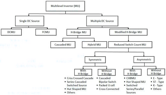
Figure 1.
Classification of multilevel inverters.
Several remarkable topologies have been developed in view of overcoming the drawbacks of conventional MLIs, such as higher switch count, input sources, capacitors, and clamping diodes [1,2,3]. A basic topology with symmetric structure and an advanced topology with both symmetric and asymmetric structures are developed. These topologies reduce the number of switches, conduction losses, and gate drivers, achieving higher efficiency and superior output performance [4]. In [5], a 17-level asymmetric topology used with a constant power standalone solar energy conversion system is proposed. The same topology provides 13 levels with a symmetric structure. A nine-level inverter is constituted with a single input source, and the others are virtual DC sources by capacitors. The topology claims a reduction in the DC source count for higher levels. However, capacitor balancing is a challenging one in producing balanced voltage levels [6]. A 17-level switched-capacitor multilevel inverter (SCMLI) is developed without using an H-bridge, reducing switches and capacitors while maintaining high performance. The design achieves efficient capacitor charging and high voltage gain with minimal conduction paths [7]. A new 31-level inverter with 12 switches is formulated with only two DC sources. The configuration can be utilized for an induction motor-based electric vehicle, where the total harmonic distortion (THD) generated in the induction motor significantly impacts the Electric Vehicles’ performance [8]. A novel crisscross augmented ladder (CCAL) structured MLI has been proposed, capable of operating in symmetric and asymmetric configurations with binary and ternary voltage ratios [9]. A double-level high-resolution multilevel inverter topology, utilizing a single DC source, is introduced, incorporating an optimized combination of switches to overcome the practical constraints in inverter applications [10].
The cross-switched topology comprises four input sources (DC) and nine switching devices for an unequal voltage input source structure used to generate 17 levels. The topology can be cascaded to achieve maximum voltage levels [11]. A new MLI structure with fewer switches and three input sources is suggested to generate a 15-level output voltage and is suitable for Photovoltaic (PV) source and industrial loads applications [12]. A new structure for MLI is developed for the single-phase 31-level MLI, accompanied by a reduced switch count. It produces a 31-level output voltage with unequal input sources and an H-bridge inverter [13]. A hybrid cascaded H-Bridge MLI topology is developed to produce 17 levels. The inverter employs staircase Pulse Width Modulation (PWM) technique [14]. A two-stage MLI using a three-level boost converter and a switched DC source MLI is developed for PV applications. The PV voltage is regulated using the boost converter, and a 21-level output voltage is produced from a switched DC source MLI [15].
A new cross-connected compact switched capacitor cell is suggested using four switches and two diodes for connecting the input DC sources and floating capacitors for multilevel inverter applications. The voltage balancing issue is to be addressed due to the use of floating capacitors [16]. An ample review of five-level MLI-based PV systems is carried out, which mainly focuses on the structure, various modulation techniques, and control techniques for grid synchronization [17]. A comprehensive review of grid-connected inverter systems reveals that efficiency improvements beyond 98% often come with higher costs and reduced reliability. Emerging designs such as HERIC and H5 inverters mitigate leakage currents and enhance overall performance [18]. A simplified nine-level switched-capacitor inverter is introduced, providing a four-fold voltage boost through just eleven switches, two capacitors, and a single diode. The circuit’s self-charging mechanism enables smooth operation in both standalone and grid-connected modes [19]. A transformer-less single-phase multilevel solar inverter with voltage boosting is introduced for efficient grid integration. It combines a partially rated DC–DC boost stage with a multilevel SPWM inverter, eliminating the need for capacitor balancing and transformers. The system achieves low losses, near-sinusoidal output, and reduced filtering requirements, ensuring cost-effective solar power conversion [20].
An assistive grid power scheme is introduced to manage severe imbalance by drawing supplemental power from the grid. The proposed approach improves system reliability and maintains power quality in a cascaded H-Bridge multilevel inverter [21]. A modular multilevel converter is proposed for integrating large-scale solar PV plants with medium-voltage grids around 11 kV. Using trinary (1:3) PV voltage modules, the system achieves 17-level voltage with improved power quality and reduced total standing voltage [22]. A single-phase transformerless inverter suitable for PV applications is proposed. The inverter operates with the flying capacitor technique and produces a five-level output with leakage current reduction [23]. An extensive analysis of multilevel inverter (MLI) topologies and control strategies for grid-connected applications is presented. It classifies diverse MLI configurations, discusses various control reference frames, and summarizes recent advancements and innovations in inverter design and performance for renewable energy systems [24]. An asymmetrical eleven-level multilevel inverter is proposed, which enables the integration of distributed power generation into the grid. This inverter utilizes a proportional-resonant controller based on current control logic [25]. Some classical designs [26,27] form the foundation for many reduced-switch topologies [28,29], which inspired recent compact inverter developments.
Based on the literature review, it is understood that the multilevel inverter is one of the pioneering technologies in the field of Power Electronics and its applications. Since the existing solutions are inadequate in terms of reducing voltage stress on the switches, decreasing control and modulation complexity, reducing harmonic distortion, and increasing the power quality, the development of new MLI topologies is essential. To address these challenges, this paper introduces a reconfigurable 10 kW string inverter topology designed for unified symmetric and asymmetric multilevel AC grid integration.
The proposed architecture minimizes the number of switches and gate drivers, shortens the conduction path, reduces voltage stress on the semiconductor devices, and enhances overall conversion efficiency. The analytical, simulation, and experimental investigations supporting the proposed system are also presented. By cascading two such proposed modules, a new variant in the cascaded MLI family is suggested. An H-Bridge inverter is concatenated with the developed cell to offer both positive and negative levels. Four distinct algorithms are introduced to decide the values of input sources (DC) for asymmetrical operation.
The key objectives of this research are as follows:
- To develop a compact Gable MLI structure topology adapted to a reconfigurable string inverter topology for a 10 kW system with a data acquisition system.
- To design a simple multi-carrier—PWM technique that reduces switching frequency and conduction path.
- To analytically assess and compare key parameters such as voltage stress, conduction losses, and harmonic distortion characteristics.
- To develop a hardware proof of concept integrated with IoT and to acquire real-time data for validating the proposed topology.
An exhaustive comparison study is carried out between the suggested cascaded MLI and its proposed algorithms with the recent topologies. The dominant features of the developed gable-shaped topology are presented in Figure 2.
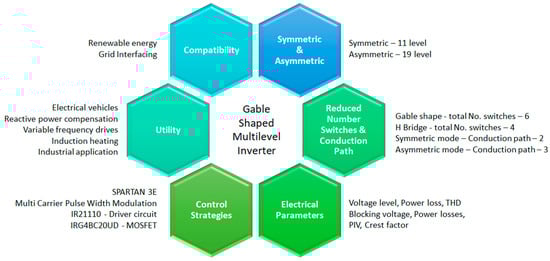
Figure 2.
Features of the proposed gable-shaped MLI.
The structure of the paper is as follows: the operating principle of the proposed MLI topologies, derivation of mathematical relationships, comparison between the existing and proposed topologies, and calculation of power losses are highlighted in Section 2. In Section 3, the simulation results and the hardware results with an integrated data-acquisition system capable of delivering 10 kW of real power and handling up to 50% overload are presented. The article is concluded in Section 4.
2. Proposed Gable-Shaped Symmetric and Asymmetric Topologies
2.1. Circuit Description and Operation
Figure 3 presents the proposed voltage generation modules for symmetrical and asymmetrical operations composed of five DC input sources arranged in a gable shape. All the switches used in these topologies are unidirectional switches. The primary purpose of this arrangement is to lessen the total number of switches conducted at each step of the output voltage. The output voltage levels generated in the proposed modules are positive levels only, and therefore, an H-Bridge can be used to generate negative cycles for an AC output. This gable-shaped structure will act as a voltage multiplier circuit for the H-Bridge inverter. Figure 3a shows that switches SW1, SW2, SW3, and SW4 must not be turned ON simultaneously to prevent the DC sources V1–V3 from short-circuiting. Similarly, the switches SW4, SW5, and SW6 must not be turned ON simultaneously to prevent a short circuit fault between the voltage sources V4 and V5.
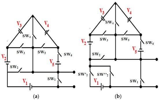
Figure 3.
Proposed gable-shaped arrangement of DC sources module (a) symmetrical (b) asymmetrical.
The DC sources can be obtained using battery or Photovoltaic (PV) sources to generate a staircase voltage waveform. The proposed structure is suitable for non-conventional energy applications. The addition of two switches with input source V1 in the symmetrical module presented in Figure 3a enables the connection or bypass of voltage sources V2–V5 to configure the proposed module for asymmetrical operation under a binary ratio (1:2) as depicted in Figure 3b. Figure 4a–f shows the various operating modes for symmetric operation, whereas the modes of operation for asymmetric operation are shown in Figure 5a–c. These structures are able to generate only positive levels; therefore, an H-Bridge inverter is required to acquire the negative levels also. In the symmetrical module, only one switch is required to conduct for each level of voltage generation, thereby reducing conduction losses, and in the asymmetrical module, two switches conduct for each voltage level. Table 1 presents the switching states to extract 11 possible voltage levels using the proposed Symmetrical structure, and Table 2 represents the Asymmetrical operating modes to acquire 19 possible voltage levels using an H-Bridge inverter.
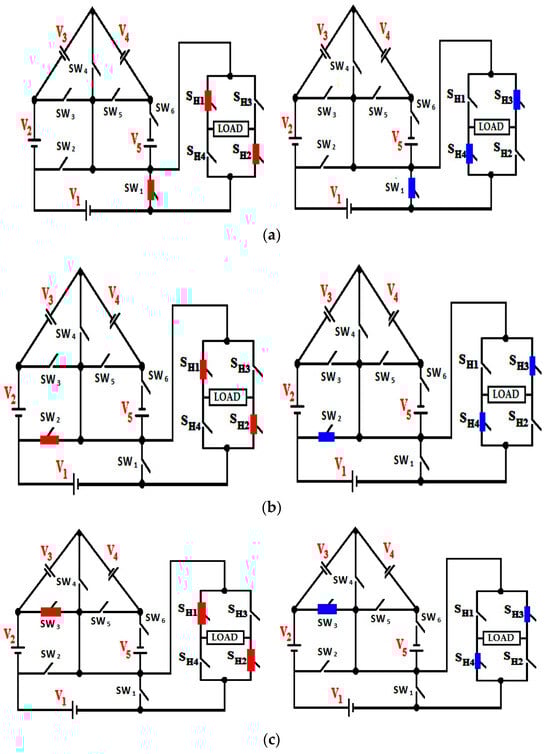
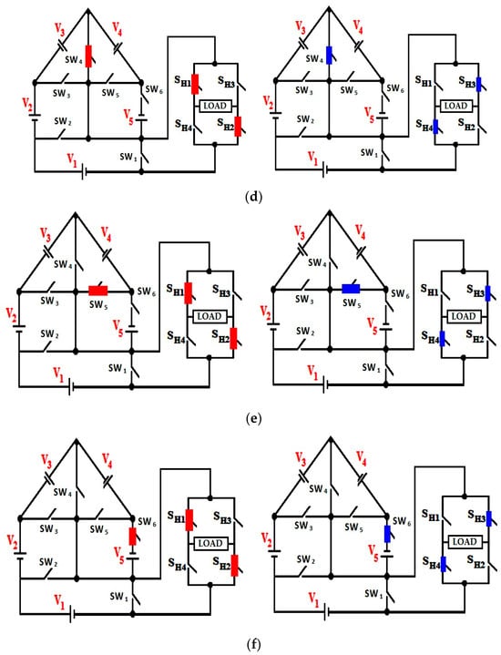
Figure 4.
Conduction states for different modes of operation of symmetrical topology. (a) Level 0, Voltage = 0. (b) Level ± 1, Voltage = ±V1. (c) Level ± 2, Voltage = ±(V1 + V2). (d) Level ± 3, Voltage = ±(V1 + V2 + V3). (e) Level ± 4, Voltage = ±(V1 + V2 + V3 + V4). (f) Level ± 5, Voltage = ±(V1 + V2 + V3 + V4 + V5).
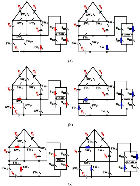
Figure 5.
Conduction states for different modes of operation of asymmetrical topology. (a) Level 0, Voltage = 0. (b) Level ± 1, Voltage = ±V1. (c) Level ± 2, Voltage = ±V2.

Table 1.
Switching sequence for 11-level output (symmetrical mode).
Table 2.
Switching sequence for 19-level output (asymmetrical mode).
The total switch count in the developed symmetrical and asymmetrical cascaded modules for attaining any voltage level is given by [(6 × h) + 4] and [(8 × h) + 4], respectively, and the number of Separated DC sources (SDC) is specified as (5 × h) where ‘h’ is the number of modules used. It is mandatory to compute the device standing voltage in the suggested modules to decide the inverter cost. In this viewpoint, the magnitude of each input source decides the blocking voltage across each device in the proposed symmetrical/asymmetrical modules, and is obtained as:
2.2. Derivation of Mathematical Relations for Different Algorithms
The cascaded symmetrical topological arrangement is pictured in Figure 6a. It is possible to achieve greater levels of voltage by utilizing various voltage magnitudes in the proposed module of asymmetrical configuration. Therefore, a half-bridge is added with the proposed symmetrical module to achieve more levels. The topological arrangement of the asymmetrical configuration is shown in Figure 6b. Four distinct algorithms have been presented for the symmetrical module to fix the magnitude of the input voltages to acquire higher levels of voltage. Table 3 tabulates the mathematical calculations to compute input source magnitudes in each module, output voltage levels, peak output voltage, and total blocking voltage of the cascaded topology using symmetrical modules. The fifth algorithm is designed for cascaded topology using asymmetrical modules only excluding the half-bridge source, and mathematical relations are portrayed in Table 4.
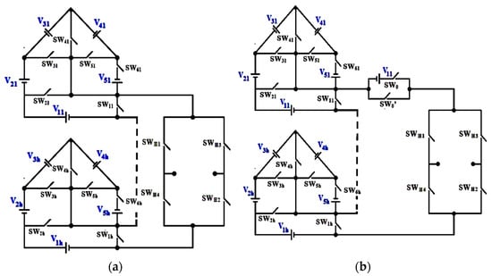
Figure 6.
(a) Cascaded symmetrical topology. (b) Cascaded asymmetrical topology.
Table 3.
Mathematical relations for asymmetrical topology using symmetrical module.
Table 4.
Mathematical relations for asymmetrical topology using asymmetrical module.
From Table 3, it is observed that using the algorithms A2, A3, and A4, the value of the dc voltage sources is different, making an asymmetrical topology with the proposed module, which results in higher voltage levels than the developed symmetrical structure for an equal number of DC sources. Table 5 tabulates the values of input voltage sources for 3 ladders using the proposed module with four algorithms. It is apparent that the number of switches and input source counts are fixed for the obtained voltage sources’ magnitudes using the proposed algorithms. Figure 7, Figure 8 and Figure 9 show the variation in maximum levels of voltage, peak output voltages, and total blocking voltages against proposed voltage source modules with proposed voltage magnitude determination algorithms. From these charts, the proposed MLI enlightens its merits in terms of lower blocking voltage with more voltage levels and is well-suited for medium voltage systems. The algorithm (A3) results in more voltage levels for large-voltage generation modules in number. However, the algorithm (A4) results in a larger number of output voltage levels with fewer modules at low blocking voltage. Figure 10 shows the graph between total switches and gate drivers against modules. Nowadays, bi-directional switches are available with higher voltage ratings, and in this study, the bi-directional devices are configured using two back-to-back unidirectional switches. Similarly, the algorithm (A5) is studied for various numbers of asymmetrical modules, resulting in the gradual increase in voltage levels with lesser blocking voltage, as shown in Figure 11.
Table 5.
Exploration of voltage source magnitudes for symmetrical module cascaded topology using proposed algorithms.
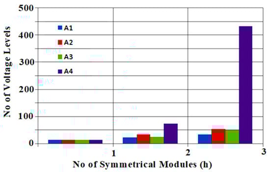
Figure 7.
Variation in the number of voltage levels against the symmetrical modules cascaded structure using the proposed algorithms.
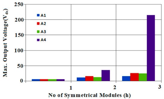
Figure 8.
Variation in Maximum output voltage against symmetrical module cascaded structure using proposed algorithms.
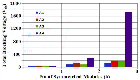
Figure 9.
Variation in total blocking voltage against symmetrical modules cascaded structure using proposed algorithms.
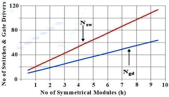
Figure 10.
Comparison of total switching devices and gate drivers against proposed symmetrical modules.
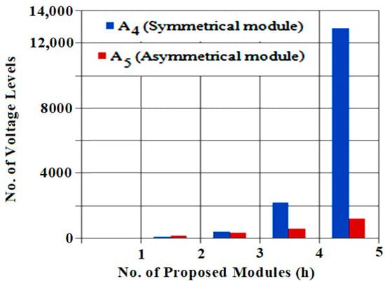
Figure 11.
Comparison between proposed algorithms (A4) and (A5) in terms of voltage levels.
2.3. Comparison Study Between Proposed and Recent Topologies
By contrasting the suggested MLI with recently produced MLIs, it is beneficial to examine the suggested MLI’s advantages. In this part, the algorithm (A4) that provides greater voltage levels with a certain number of recommended voltage-generating modules (h) is used to examine the suggested MLI structure employing symmetrical modules.
The recent topologies available in the literature consider both symmetrical and asymmetrical operations to compare different parameters in terms of switches, gate drivers, and the minimum number of sources to produce the required voltage levels. The topologies developed in [26,28,29,30] are considered with their asymmetrical operations using their voltage determination algorithms, and the symmetrical topologies presented in [27,31,32] are taken for comparison study. It is observed from Figure 12, Figure 13 and Figure 14 that the suggested topology needs the minimum number of input sources, switches, and gate drivers while increasing the levels of voltage.
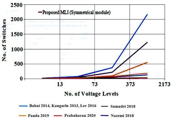
Figure 12.
Comparison of the number of switches against voltage levels [26,27,28,29,30,31,32].
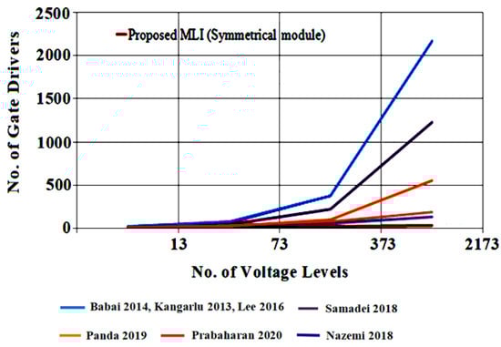
Figure 13.
Comparison of gate drivers against voltage levels [26,27,28,29,30,31,32].
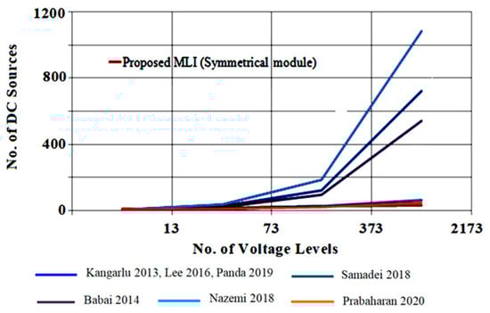
Figure 14.
Comparison of the number of DC sources required against voltage levels [26,27,28,29,30,31,32].
The choice of voltage source magnitudes determines the device blocking voltage, which in turn affects the implementation cost for achieving higher voltage levels. In both the presented symmetrical and asymmetrical modules, the advantages lie in their ability to generate different voltage levels based on the chosen voltage ratio. The selection of an appropriate algorithm plays a crucial role in achieving higher voltage levels while using devices with lower blocking voltage ratings. Table 6 presents the comparison of the proposed topology with other topologies in terms of the number of voltage sources, the number of voltage levels, the number of switches used, and the current conduction paths. From this table, it is noticeable that the gable-shaped topology uses fewer paths for current conduction when compared to other topologies.
Table 6.
Comparison of different MLI topologies with the proposed topology.
2.4. Calculation of Losses
The other important factor in performance indices is the power incurred by switching devices at the time of turn-on and turn-off, and the value of total load current over one switching cycle. The suggested topology needs less switch count in the current conduction path compared with its counterparts, and only one switch performs Pulse Width Modulation (PWM) switching, and the remaining two switches in the H-Bridge inverter are switched at fundamental switching. The transition loss occurs during the change from off state to on state over the course of a single fundamental switching cycle.
Also, the static loss during conduction remains constant for the given operating switching frequency (fs) while the transition loss varies with respect to switching frequency.
The transition loss of the ‘ith’ switch is given in Equation (7)
The suggested structure can be implemented to attain greater voltage levels with reduced switching loss when compared with the Cascaded H-Bridge MLI. The average switching loss for an 11-level inverter with DC source voltages equal to Vdc is provided in Equation (8)
where
The TON and TOFF values are assumed to be identical for each switch during the conduction of the load current (Io). Consequently, the switching loss is estimated in Equation (10) as
where γ represents a constant,
the conduction losses of IGBT switches can be estimated by Equation (12) as
where
- VD—Forward Voltage drop of the IGBT switch
- RSW—On-state switching resistance
- I(t)—RMS output current, β—Switch specification constant
Thus, the overall power losses can be calculated as,
the output power of the suggested inverter can be calculated as,
where VO and IO are the rms output voltage and rms output current.
The efficiency can be calculated as,
3. Simulation and Experimental Study
3.1. Simulation Results
The operational topologies of the suggested MLI for both symmetrical and asymmetrical modules are analyzed using MATLAB/Simulink in ideal conditions with one module. The input source voltage values are selected for symmetrical and asymmetrical modules to produce 11-and 19-level inverter voltage with a peak value of 300 V across an RL Load of 150 Ω and 100 mH. The input voltage values are taken as (V1 = V2 = V3 = V4 = V5 = 60 V) for symmetrical module and (V1 = 33 V; V2 = V3 = V4 = V 5= 67 V) for asymmetrical module in simulation study. The switching and carrier frequencies to generate the required PWM pulses are taken as 2 kHz and 50 Hz using the Multi Carrier Pulse Width Modulation-Phase Disposition (MCPWM-PD) strategy. The MCPWM-PD strategy is comparatively simple to implement when the number of voltage levels is more. Also, for modular multilevel inverter topologies, it ensures a balanced operation such that all inverter cells operate with the same switching frequency and loss. Figure 15, Figure 16 and Figure 17 portray the pulse pattern, load voltage with voltage spectrum, and load current for the 11-level inverter. Similarly, Figure 18, Figure 19 and Figure 20 represent pulse pattern, load voltage with voltage spectrum, and load current for a 19-level inverter. These Figures illustrate that the Total Harmonic Distortion (THD) of the output voltage is 5.78% for symmetrical topology and 3.69% for asymmetrical topology during simulation. This demonstrates that the THD decreases while changing from 11 to 19 level inverter operations for the same fundamental output voltage. A similar trend is observed in the hardware results.
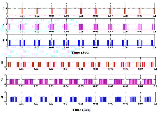
Figure 15.
Gating pulses for an 11-level inverter.
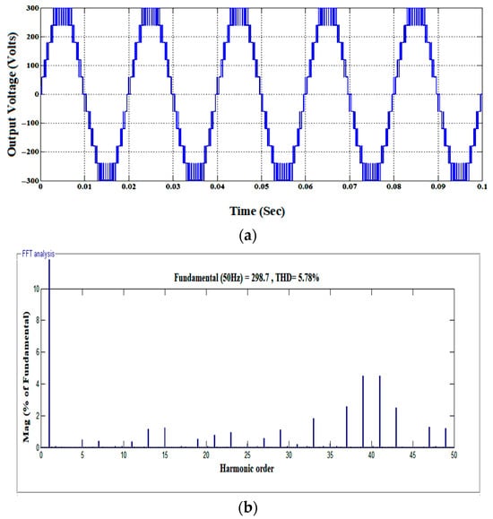
Figure 16.
Simulation results (a) Output voltage for an 11-level inverter. (b) Voltage spectrum for an 11-level inverter.
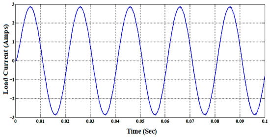
Figure 17.
Load current for the 11-level inverter.
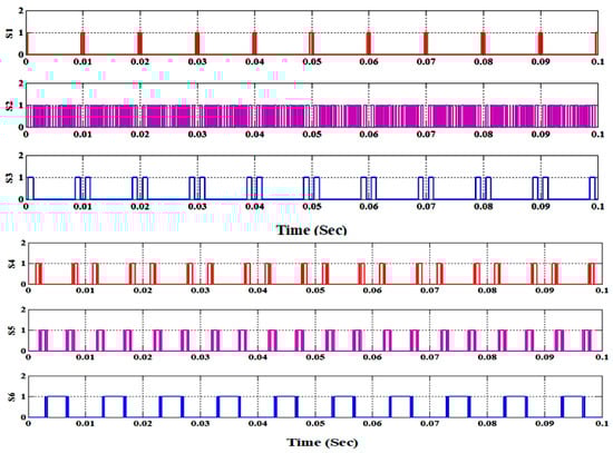
Figure 18.
Gating pulses for a 19-level inverter.
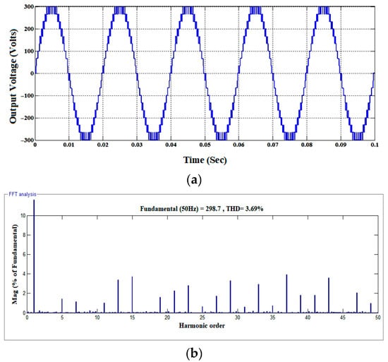
Figure 19.
Simulation results (a) Output voltage for the 19-level inverter. (b) Voltage spectrum for a 19-level inverter.
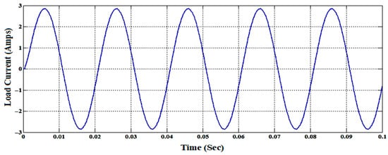
Figure 20.
Load current for the 19-level inverter.
3.2. Experimental Results for Gable-Shaped MLI
The simulation results attained from MATLAB/Simulink are experimentally validated using a laboratory model presented in Figure 21, constructed using IGBTs (IRG4BC20UD) and a gate driver IC (IR2110) circuit for pumping the voltage signals to the required threshold level to the gate of IGBTs. The input and load specifications are the same as those of the simulation, and the gating signals are acquired from the FPGA Xilinx Spartan 3E controller. The methodology uses Look-Up Tables of sinusoidal and triangular signals, which are directly compared to generate base PWM pulses at each voltage level.
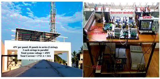
Figure 21.
Experimental prototype of the proposed topology.
The VHDL coding is used to formulate the algorithm and to generate the required PWM pulses from base PWM and logical operations. The method looks simple for open-loop operation and can be extended for any voltage levels. Figure 22 and Figure 23 depict load voltage along with voltage spectrum and load current for 11-and 19-level inverters. The experimental results have a close relation with their simulation results.
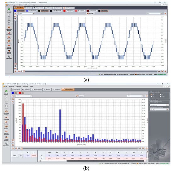
Figure 22.
Hardware results (a) Output voltage for an 11-level inverter. (b) Voltage spectrum for an 11-level inverter.
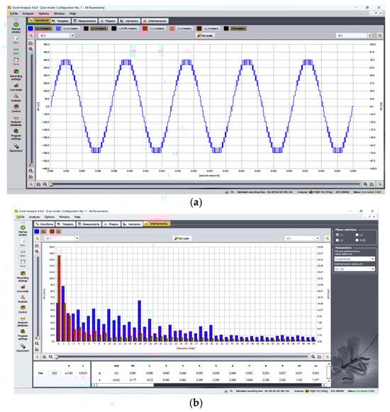
Figure 23.
Hardware results (a) Output voltage for a 19-level inverter. (b) Voltage spectrum for a 19-level inverter.
3.3. Experimental Results for Gable-Shaped MLI with Grid Interfacing
The proposed gable-shaped MLI structure has been interfaced with a grid under steady-state operation, injecting 10 kW of active power. The corresponding voltage variations are shown in Figure 24a,b shows the current waveform of grid-connected operation of the 19-level inverter in steady-state power transfer conditions.
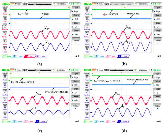
Figure 24.
(a–d) Real-time results of grid-connected operation of the 19-level inverter in a steady-state condition under power transfer conditions with 10 kW of active power.
Figure 24c provides the real-time results of grid-connected operation with 10 kW active power and 10 kVAR reactive power. Figure 24d illustrates the real-time results under balanced load conditions for the 19-level inverter in steady-state grid-connected operation. The performance of the grid-connected 19-level inverter is also evaluated under varying power conditions.
The power injected into the grid is varied from 10 kW to 15 kW, and the corresponding variations are shown in Figure 25a–f. The components used for the grid-connected operation of the 19-level asymmetrical inverter topology are listed in Table 7. The corresponding switching loss and conduction loss are calculated from the circuit and tabulated in Table 8. The overall efficiency is calculated considering the total switching and conduction losses. The total switching and conduction losses are 31.2 W while delivering a 10 kW output power to the grid, and hence the efficiency is found to be 98.46%.
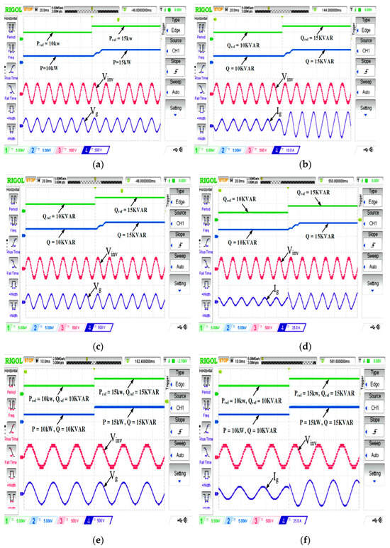
Figure 25.
(a–f) grid-connected operation of the 19-level inverter when injected power is increased to double (a,b) 10 kW active power to 15 kW (c,d) 10 kVAR reactive power to 15 kVAR, and (e,f) 10 kW, 10 kVAR to 15 kW, 15 kVAR active and reactive power.
Table 7.
Components used for the grid operation of a 19-level asymmetrical inverter topology.
Table 8.
Switching and conduction losses while transferring power to the grid at 10 kW.
Figure 26 illustrates the real-time operational performance of a 10 kWp distributed Grid system. It includes details of plant information, live power generation (6.92 kW), daily and monthly production trends, environmental benefits (CO2 reduction and equivalent trees planted), and irradiance-based performance statistics for 13 October 2025). The online monitoring dashboard, integrated with a VSN700 data logger, provides real-time visualization and performance tracking of the 10 kW grid-tied solar PV plant installed. The system continuously records critical parameters such as DC voltage and current from PV strings, AC power output, inverter temperature, solar irradiance, and ambient conditions. The dashboard interface presents instantaneous, daily, monthly, and yearly performance metrics, including power generation, grid feed-in, and energy consumption data. Key performance indicators such as daily energy yield, system efficiency, and CO2 emission reduction are automatically computed and displayed, offering a clear assessment of plant productivity.
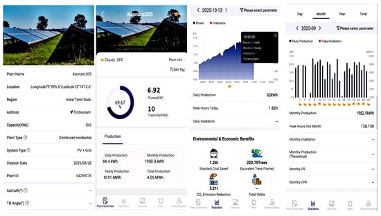
Figure 26.
Solar PV plant monitoring dashboard online monitoring with VSN700 data logger.
Figure 27 presents the inverter-level monitoring details of the 10 kWp PV + Grid system. It includes monthly generation and grid feed statistics, DC and AC side electrical parameters, temperature readings of inverter components, and operational state information showing the inverter connected to the grid. Each inverter’s electrical behavior is monitored individually to identify string mismatches or operational faults, ensuring reliable and efficient performance. Additionally, the system estimates the environmental impact in terms of equivalent trees planted and carbon offset achieved. With cloud connectivity provided by the VSN700, users can remotely access plant data, receive maintenance alerts, and analyze long-term trends through web or mobile platforms. This monitoring setup not only enhances operational reliability but also facilitates fault detection, performance optimization, and future integration with hybrid microgrid or energy storage systems.
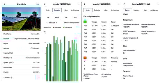
Figure 27.
Inverter-level monitoring details of the 10 kWp PV + grid system.
4. Conclusions
In this article, two novel voltage-generation modules with symmetrical and asymmetrical operations are proposed to reduce the total number of switching devices in the current conduction path while increasing voltage levels for AC micro-grid applications. The symmetrical module, employing five DC sources in a gable-shaped configuration, is designed to minimize current conduction paths and ensure equal voltage source distribution. The asymmetrical module incorporates two additional switches to isolate or connect the first voltage source, enabling a voltage source ratio of 1:2:2:2:2. This configuration significantly increases the output voltage levels while maintaining fewer switches in the conduction path.
The proposed topologies were validated through MATLAB simulations, achieving THD values of 5.78% and 3.69% for the symmetric and asymmetric configurations. These topologies effectively reduce voltage stress on switches through conduction path curbing, while also lowering complexity, making them suitable for grid-connected systems. The practicality of the topologies is verified using a Hardware-in-the-Loop setup with an integrated data-acquisition system capable of delivering 10 kW of real power and handling up to 50% overload. These results confirm the suitability of the topology for real-time grid applications. Further research is recommended to optimize control strategies, enhance scalability, and improve reliability for higher-power applications.
Author Contributions
Conceptualization, B.V. and K.C. and S.T.J.; methodology, B.V., K.C. and S.T.J.; software, B.V.; validation, B.V., K.C. and S.T.J.; formal analysis, B.V., K.C. and S.T.J.; investigation, B.V.; resources, K.C.; data curation, K.C.; writing—original draft preparation, B.V. and K.C.; writing—review and editing, K.C.; supervision, K.C. and S.T.J.; project administration, K.C. and S.T.J.; funding acquisition, K.C. and S.T.J. All authors have read and agreed to the published version of the manuscript.
Funding
This research received no external funding.
Data Availability Statement
The original contributions presented in this study are included in the article. Further inquiries can be directed to the corresponding author.
Acknowledgments
The authors extend their heartfelt gratitude to the esteemed management of KCG College of Technology, Chennai, India and M.Muthukannan, Principal of KCG College of Technology. Their unwavering support, guidance, and commitment to academic excellence have been invaluable throughout the research process. We are particularly thankful for their encouragement in fostering an environment that promotes learning and research endeavors. This acknowledgement serves as a token of appreciation for their instrumental roles in our academic journey.
Conflicts of Interest
The authors declare no conflicts of interest.
References
- Al-Hitmi, M.A.; Hussan, M.R.; Iqbal, A.; Islam, S. Symmetric and Asymmetric Multilevel Inverter Topologies with Reduced Device Count. IEEE Access 2023, 11, 5231–5245. [Google Scholar] [CrossRef]
- Shakeera, S.; Rachananjali, K. An Innovative 11-Level Multilevel Inverter Topology with Rotating Trapezoidal SPWM for Industrial and Renewable Applications. Sci. Rep. 2024, 14, 22359. [Google Scholar] [CrossRef]
- Nyamathulla, S.; Chittathuru, D. A Review of Multilevel Inverter Topologies for Grid-Connected Sustainable Solar Photovoltaic Systems. Sustainability 2023, 15, 13376. [Google Scholar] [CrossRef]
- Radmanesh, H.; Seifi, A. New Generalized Multilevel Inverter Based on Developed H-Bridge with Reduced Circuit Component. IEEE Access 2025, 13, 165587–165597. [Google Scholar] [CrossRef]
- Nirmal Mukundan, C.M.; Al-Durra, A.; Vineeth, K.; Jayaprakash, P.; El-Fouly, T.H.M.; Zeineldin, H.H. A New Multilevel Inverter with Reduced Component Count for a Standalone Solar Energy Conversion System. IEEE Trans. Ind. Appl. 2024, 60, 3247–3262. [Google Scholar] [CrossRef]
- Hassan, A.; Yang, X.; Chen, W. Single and Double Input DC Sources Multilevel Inverter Topologies with Reduced Components Counts and Voltage Boosting Property for Grid-Connected Photovoltaic Converters. IEEE J. Emerg. Sel. Top. Power Electron. 2022, 10, 7704–7720. [Google Scholar] [CrossRef]
- Roy, T.; Nandi, S.; Patel, R.; Misra, B.; Nayak, B. Investigation of an Extendable Multisource Switched-Capacitor Multilevel Inverter with Reduced Device Count. IEEE J. Emerg. Sel. Top. Power Electron. 2025, 13, 3013–3027. [Google Scholar] [CrossRef]
- Saravanan, K.; Sivasubramanian, M.; Gopinath, N.P.; Kumarasamy, K.; Azhagumurugan, R. A 31-Level Multilevel Inverter Topology with Less Switching Devices for Hybrid Electric Vehicle Applications. Sci. Rep. 2024, 14, 27459. [Google Scholar] [CrossRef]
- Arumugam, P.; Subbaraman, S.; Chandrasekaran, S. Symmetric and Asymmetric Crisscross Augmented Ladder Multilevel Inverter with Fuzzy Logic Controller Optimization. Symmetry 2023, 15, 1366. [Google Scholar] [CrossRef]
- Tak, N.; Chattopadhyay, S.K.; Chakraborty, C. Single-Sourced Double-Stage Multilevel Inverter for Grid-Connected Solar PV Systems. IEEE Open J. Ind. Electron. Soc. 2022, 3, 561–581. [Google Scholar] [CrossRef]
- Kakar, S.; Ayob, S.B.M.; Iqbal, A.; Nordin, N.M.; Arif, M.S.B.; Gore, S. New Asymmetrical Modular Multilevel Inverter Topology with Reduced Number of Switches. IEEE Access 2021, 9, 27627–27637. [Google Scholar] [CrossRef]
- Samanbakhsh, R.; Ibanez, F.M.; Koohi, P.; Martin, F. A New Asymmetric Cascaded Multilevel Converter Topology with Reduced Voltage Stress and Number of Switches. IEEE Access 2021, 9, 92276–92287. [Google Scholar] [CrossRef]
- Prasad, D.; Dhanamjayulu, C.; Padmanaban, S.; Holm-Nielsen, J.B.; Blaabjerg, F.; Khasim, S.R. Design and Implementation of 31-Level Asymmetrical Inverter with Reduced Components. IEEE Access 2021, 9, 22788–22803. [Google Scholar] [CrossRef]
- Dhanamjayulu, C.; Prasad, D.; Padmanaban, S.; Maroti, P.K.; Holm-Nielsen, J.B.; Blaabjerg, F. Design and Implementation of 17-Level Inverter with Reduced Components. IEEE Access 2021, 9, 16746–16760. [Google Scholar] [CrossRef]
- Khasim, S.R.; Dhanamjayulu, C.; Padmanaban, S.; Holm-Nielsen, J.B.; Mitolo, M. A Novel Asymmetrical 21-Level Inverter for Solar PV Energy System with Reduced Switch Count. IEEE Access 2021, 9, 11761–11775. [Google Scholar] [CrossRef]
- Jagabar Sathik, M.; Sandeep, N.; Almakhles, D.; Blaabjerg, F. Cross Connected Compact Switched-Capacitor Multilevel Inverter (C3-SCMLI) Topology with Reduced Switch Count. IEEE Trans. Circuits Syst. II Express Br. 2020, 67, 3287–3291. [Google Scholar] [CrossRef]
- Tiwari, A.; Kumar, V.; Agarwal, R.; Amir, M.; Alharbi, M.A.; Muyeen, S.M. Five-Level MLI-Based Grid-Connected Photovoltaic Systems: A Review on Control Methodologies, Modulation Strategies and Recent Developments. IEEE Open J. Power Electron. 2025, 6, 78–108. [Google Scholar] [CrossRef]
- Pudur, R.; Rajak, M.K. A Comprehensive Review of Grid-Connected Inverter Topologies and Control Strategies (2020–2025). Next Energy 2025, 9, 100433. [Google Scholar] [CrossRef]
- Ali, M.; Tayyab, M.; Sarwar, A.; Abido, M.A.; Khalid, M. Standalone and Grid-Connected Operation of Single-Source Multilevel Inverter with Boosted Output Voltage. Alex. Eng. J. 2024, 103, 278–287. [Google Scholar] [CrossRef]
- Chakraborty, S.; Sarkar, K.; Maiti, D.; Chakrabarti, A.; Dasgupta, S.; Biswas, S.K. A Single-Phase Grid-Tied Transformer-Less Multilevel Solar Inverter with Voltage Boost. IEEE Trans. Ind. Electron. 2025. Early Access. [Google Scholar] [CrossRef]
- Tanguturi, J.; Keerthipati, S. Assistive Grid Power Scheme to Enhance Power Balancing Capacity of Solar Photovoltaic CHB Inverter for Grid-Connected Application. IEEE Trans. Ind. Electron. 2025, 72, 9207–9216. [Google Scholar] [CrossRef]
- Yadav, S.K.; Singh, B. Analysis and Grid-Tied Implementation of Seventeen Level Utility-Scale SPV Configuration Considering Real-Time Geographical Irradiance. IEEE J. Emerg. Sel. Top. Ind. Electron. 2025, 6, 175–183. [Google Scholar] [CrossRef]
- Zhu, X.; Wang, H.; Zhang, W.; Wang, H.; Deng, X.; Yue, X. A single-phase five-level transformer-less PV inverter for leakage current reduction. IEEE Trans. Ind. Electron. 2022, 69, 3546–3555. [Google Scholar] [CrossRef]
- Salem, M.; Richelli, A.; Yahya, K.; Hamidi, M.N.; Ang, T.Z.; Alhamrouni, I. A Comprehensive Review on Multilevel Inverters for Grid-Tied System Applications. Energies 2022, 15, 6315. [Google Scholar] [CrossRef]
- Tayyab, M.; Sarwar, A.; Murshid, S.; Tariq, M.; Urooj, S.; Khan, B. Grid-connected operation and control of single-phase asymmetrical multilevel inverter for distributed power generation. IET Renew. Power Gener. 2022, 16, 3629–3642. [Google Scholar] [CrossRef]
- Babaei, E.; Laali, S.; Alilu, S. Cascaded Multilevel Inverter with Series Connection of Novel H-Bridge Basic Units. IEEE Trans. Ind. Electron. 2014, 61, 6664–6671. [Google Scholar] [CrossRef]
- Kangarlu, M.F.; Babaei, E. A Generalized Cascaded Multilevel Inverter Using Series Connection of Sub multilevel Inverters. IEEE Trans. Power Electron. 2013, 28, 625–636. [Google Scholar] [CrossRef]
- Samadaei, E.; Sheikholeslami, A.; Gholamian, S.A.; Adabi, J. A Square T-Type (ST-Type) Module for Asymmetrical Multilevel Inverters. IEEE Trans. Power Electron. 2018, 33, 987–996. [Google Scholar] [CrossRef]
- Nazemi Babadi, A.; Salari, O.; Mojibian, M.J.; Bina, M.T. Modified Multilevel Inverters with Reduced Structures Based on Packed U-Cell. IEEE J. Emerg. Sel. Top. Power Electron. 2018, 6, 874–887. [Google Scholar] [CrossRef]
- Prabaharan, N.; Salam, Z.; Cecati, C.; Palanisamy, K. Design and Implementation of New Multilevel Inverter Topology for Trinary Sequence Using Unipolar Pulse width Modulation. IEEE Trans. Ind. Electron. 2020, 67, 3573–3582. [Google Scholar] [CrossRef]
- Panda, K.P.; Lee, S.S.; Panda, G. Reduced Switch Cascaded Multilevel Inverter with New Selective Harmonic Elimination Control for Standalone Renewable Energy System. IEEE Trans. Ind. Appl. 2019, 55, 7561–7574. [Google Scholar] [CrossRef]
- Lee, S.S.; Chu, B.; Idris, N.R.N.; Goh, H.H.; Heng, Y.E. Switched-Battery Boost-Multilevel Inverter with GA Optimized SHEPWM for Standalone Application. IEEE Trans. Ind. Electron. 2016, 63, 2133–2142. [Google Scholar] [CrossRef]
Disclaimer/Publisher’s Note: The statements, opinions and data contained in all publications are solely those of the individual author(s) and contributor(s) and not of MDPI and/or the editor(s). MDPI and/or the editor(s) disclaim responsibility for any injury to people or property resulting from any ideas, methods, instructions or products referred to in the content. |
© 2025 by the authors. Licensee MDPI, Basel, Switzerland. This article is an open access article distributed under the terms and conditions of the Creative Commons Attribution (CC BY) license (https://creativecommons.org/licenses/by/4.0/).