Abstract
A voltage-controlled oscillator (VCO) is an essential part of the clock circuitry in satellite communication systems. Low-dropout regulators (LDO) provide stable voltage supply to the VCO and inevitably bring in new radiation-sensitive nodes. In this paper, by conducting single-event transient (SET) sensitivity analysis of LDO in voltage-regulated VCO, we find the sensitive nodes of LDO in oscillation circuits located on the relevant transistors that determine the bias voltage of the tail transistor in the error amplifier (EA). To immunize SET, a symmetrical hardening method combining sensitive node splitting and resistive-decoupling is proposed for the sensitive nodes. This method achieves 80.8% analog single-event transient (ASET) mitigation. This study was conducted in 28-nm CMOS process.
1. Introduction
Phase-locked loop (PLL) is widely used to generate stabilized clocking in satellite communication systems. The cosmic radiation environment that the satellite-based PLL is exposed to makes it necessary to consider radiation resistance besides performance metrics in its design [1]. The particle impaction in the cosmic environment can lead to catastrophic failure of satellite communications. The single-event effect (SEE) is caused by a single particle that deposits a certain number of charges on the silicon substrate, which instantly interferes with the operation of the integrated circuit [2]. In addition to the single-event upset (SEU), which can flip the output of a digital logic circuit, SEE includes single-event transient (SET), which propagates through the circuit [3]. SET is a voltage disturbance caused by a collected radiation-induced charge in a circuit node that travels through the circuit.
A voltage-controlled oscillator (VCO) is the core module in the PLL, and its phase noise directly affects the performance of the PLL [4]. The power supply noise is the crucial source of phase noise in the VCO [5]. Therefore, the conventional design of VCO is focused on noise suppression of the power supply. A low-dropout regulator (LDO) is a common method to provide high-quality power supply to the VCO [6,7].
LC VCO as a widely used component in high-speed communication applications, and many studies have been conducted on the SETs of LC VCO in the cosmic radiation environment [8,9,10,11,12,13,14]. When a single particle hits a sensitive node in VCO, it can lead directly to frequency deviation and signal distortion of the VCO outputs and even a temporary stop of oscillation [2,15]. LDO as a structure to suppress VCO power supply noise has been studied for its SET characteristics in different semiconductor processes [16,17]. Those studies found that loop stability [18], input voltage [19], and load conditions [20] all affect the SETs of linear regulators significantly.
Radiation Hardening by Design (RHBD) is one solution to SET mitigation. Unlike Radiation Hardening by Process (RHBP), RHBD is implemented in the CMOS process to achieve circuit-level hardening by applying a schematic and layout change.
Three-mode redundancy (TMD) is widely used in analog and mixed-signal circuit hardening, Ref. [21] used the TMD to harden the LC VCO, while Ref. [22] used this technology to harden ring VCO. It shows great hardening effects but at the cost of a significant increase in circuit surface area and power consumption. Filtering can reduce SET amplitude and duration on the circuit and system levels. Ref. [23] used filtering in LDO hardening design; however, the introduction of capacitors also increases the circuit surface area and power consumption. Ref. [24] proposed a fast transient response circuit under narrow-band conditions to improve the recovery speed of the LDO in the environment of radiation. This approach does not change the response loop in the LDO but introduces extra circuits that can be sensitive nodes. Resistive decoupling was first applied as a technique for hardening memory cells. Ref. [25] proposed an improvement in the SET response by adding a resistor in series with the base of the power transistor in the linear regulator. Ref. [26] used this method on the charge pump (CP) of PLL. Time-skewed space-split is an implementation of sensitive node-splitting technology, which is usually used to harden switched capacitor circuits. Ref. [27] used this method to harden the power transistor in LDO.
Research on the SETs of LDOs is mainly focused on commercial LDO chips and the SETs of on-chip LDOs have been less studied, especially those applied to LC VCOs. This paper analyzes the SET-sensitive nodes of LDO applicable to LC VCO and proposes a radiation-hardened LDO design based on sensitive node splitting and resistive decoupling under the restrictions of surface area and power efficiency.
2. Responses of Single-Event Transients in the LDO
2.1. PLL Architecture
At present, the commonly used PLL is based on charge pumps, and its overall topology is shown in Figure 1. In the PLL, the clock generated by the VCO is compared with the reference clock after the frequency divider (DIV), and the CP sources or sinks charges for a controlled amount of time according to the comparison signal and . The low-pass filter (LPF) responds to the pump current with voltage a jump, and controls the frequency of the signal generated by the VCO.
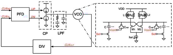
Figure 1.
Conventional charge pump phase-locked loop (CP-PLL) structure. represents the equivalent parallel resistance of the inductor in LC voltage-controlled oscillato (VCO), and controls the constant tank capacitors, C.
The source of VCO phase noise is electronic noise, power supply noise, and substrate noise; the phase noise directly determines the quality of the clock signal generated by the PLL [28]. The phase noise of the LC VCO can be expressed in Equation (1) [29]:
where is the VCO oscillation frequency, Q is the quality factor of the LC oscillator, k is the Boltzmann constant, and T is the temperature in Kelvin. Equation (1) shows that the oscillation frequency is related to all capacitors in the LC VCO, including the switch-controlled constant capacitor C, the switch-equivalent capacitor, the variable capacitor , and the drain-bulk capacitance of and . When the power supply fluctuates, all variable capacitors, including the drain-bulk capacitance of and , will be changed with the fluctuation of the power supply, thus changing the VCO output frequency , which affects the phase noise of the VCO. Simultaneously, the power supply fluctuation also changes the of the VCO, which directly affects the magnitude of the VCO output signal.
To suppress power-supply noise in VCOs, LDOs are commonly used in modern VCO designs. Any added circuit introduces extra sensitive nodes in the radiation environment; thus, SET-sensitive node analysis for the LDO is necessary. Since the LDO is used to suppress the power supply noise of the VCO and the SET-sensitive nodes in the LDO cannot be analyzed merely by considering the output voltage; therefore, the LDO and VCO need to be analyzed together.
2.2. Responses of SET in LDO
The LDO used in this study is shown in Figure 2a. The differential pair used in the error amplifier is an n-MOS transistor, and the power transistor is p-MOS transistor. SETs are simulated using a double exponential current source [30].
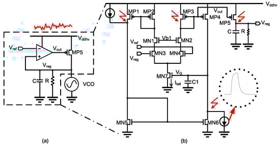
Figure 2.
Low-dropout regulator (LDO) structure: (a) Supply-regulated VCO. (b) Unhardened regulator schematic.
Figure 2b shows the implementation of the LDO circuit in this paper. A start-up circuit is not presented in the schematic. Double exponential current sources with a peak value of 2 mA and a decay time of 2 ns are injected at the drains of , , , and , respectively.
To evaluate the impact of these current pulses, the output voltage of the regulator , and the frequency of the VCO were analyzed. The simulation results are shown in Figure 3a–c.
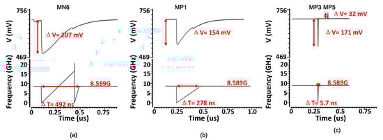
Figure 3.
Single-event transient (SET) induced disturbance in LDO output voltage and VCO oscillating frequency when the particle strike occurs on: (a) ; (b) ; (c) and .
Figure 3a shows the transient response of the LDO output voltage and VCO oscillation frequency when the particle strike occurs on the . The LDO output voltage changed from 700 mV to 493 mV, and the VCO oscillation frequency changed from GHz to zero. The oscillation recovery time was 492 ns.
Figure 3b,c present the transient simulation of the LDO output voltage and VCO oscillation frequency when the particle strike occurs on the , and . The LDO output voltage changed from 700 mV to 546 mV, 529 mV, and 732 mV, respectively. The oscillation recovery times were 278 ns and ns for and .
It can be seen that when a single particle strikes on , , and , the LDO voltage decreased, which caused the VCO to stop oscillating, exhibiting a greatly varied non-oscillating duration. To maintain the oscillation of the VCO, the tail current source in the VCO should provide enough current to meet its oscillation conditions. When the power supply of the VCO is directly connected to the main power supply, the power supply can provide enough current to keep the VCO working as long as the tail current source of the VCO is in normal condition. However, when the regulator provides the power supply to the VCO, it will cause the VCO to stop oscillating if the regulator does not work correctly when injected with charges.
The transfer function between the LDO output voltage and the LDO input voltage is shown in Equation (2).
where
Power-supply rejection ratio (PSRR) is a term that quantifies the ability of a circuit to suppress fluctuations on the power supply.
When a particle impacts the LDO, the output voltage of the LDO will change and no longer follow its reference voltage . The re-following process, realized slowly with the regulation of the loop, is closely related to the response time of the loop, which indicates that the bandwidth of the entire loop determines its regulation speed.
When a single particle hits the or , the tail transistor in the error amplifier no longer works in its saturation region, disabling the entire error amplifier. The failing error amplifier affects the power transistor in the LDO circuit, making it unable to continue working in the saturation region. Inevitably, the LDO fails to provide sufficient current to the VCO, in which case the oscillation is terminated. Under this circumstance, the PLL will not be able to lock in a significant period. It is meaningless to achieve quick recovery by improving the loop response time since the drastic change in bias conditions will not recover instantly by the feedback loop. For , SET will potentially reduce its drain voltage, causing the LDO voltage output to decrease and eventually stop the VCO. However, the working region of the is not changed, and the entire system will be immediately recovered once the particle strike is over.
3. The Proposed SET Hardened LDO Regulator
As mentioned in the previous analysis, it is essential to add an LDO regulator to the VCO in the PLL design. However, the added LDO regulator will introduce additional sensitive nodes, making the study of regulator hardening necessary. The previous analysis proved that under SET, the sensitive node inside the regulator that de-oscillates the VCO is the insufficient current source of the error amplifier. In other words, the bias voltage of the is too low to work in the saturation region, and the recovery takes time. The hardening design principle is to reduce the possibility of bias voltage being cut off and to avoid introducing additional sensitive nodes.
3.1. Proposed SET Radiation-Hardened (RH) Structure
The key to our hardening design is to reduce the possibility of being turned off or to stabilize to provide sufficient current to the differential pair transistors under single particle impaction. As Figure 4 shows, to achieve this goal, we split the required tail current into multiple parts, which are provided by different transistors (~), to ensure that they are independent of each other. When one of the transistors is impacted by a single particle and no longer provides sufficient current, other transistors still work normally.
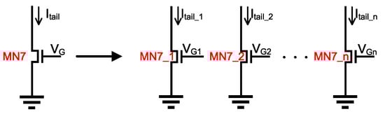
Figure 4.
Current is provided by splitting transistor .
In analog integrated circuit design, the gate width of the transistor is usually a multiple of 2 to match the layout. When we split the current , the number of current splits n must be a power of 2. The number of split parts is limited by the size of the transistors in the unhardened circuit design.
To make the split parts independent of each other, all the splits are provided by independent bias circuits. When splitting , it is necessary to split , , , and , respectively, into the same number of parts as . To further attenuate the effect of the SET on the current, resistive decoupling is adopted in this design. The splits of the same node are connected by a resistor in the middle. The current is supplied in the multi-path, and transistors are symmetrically split. The overall hardened circuit symmetrical multi-path splitting (SMPS) when transistors are split into two parts is shown in Figure 5.
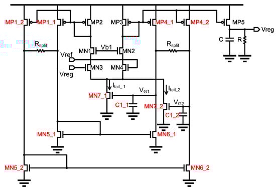
Figure 5.
Symmetrical multi-path splitting (SMPS) regulator, with a split factor .
From the previous simulation results, it can be seen that single particle impaction on either or will cause the VCO to stop oscillation for a different duration. When the single particle impaction occurs on , it takes a certain path to transmit the ; meanwhile, SET has its transfer characteristics that will be attenuated by physical distance, thus causing a relatively shorter stop of oscillation. However, the impaction on directly affects the bias of , causing a longer stop of oscillation. Since the is more sensitive to SET, we will use as an example to explain the hardening design in the following discussion.
3.2. Analysis
A comparison before and after the implementation of the hardened design of -related circuits is shown in Figure 6.
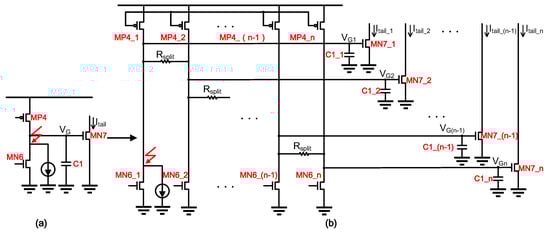
Figure 6.
(a) Unhardened related circuit; (b) symmetrical multi-path splitting (SMPS) circuit-related .
The two ends of each resistor are symmetrically connected to , , , , and , , , , and the electric potentials at both ends are and . In the absence of SET, that is, when direct current (DC) is stabilized, both ends of have the same electric potential because of the completely symmetrical circuit structure, and no current passes through .
As mentioned above, the number of splits n must be a power of two. When , the bias voltage of is provided by , and the bias voltage of is provided by . When the drain of is affected by a single particle, the voltage fluctuation occurs, and this voltage fluctuation will change the current of . To analyze the propagation of this fluctuation in the circuit, we give the equivalent circuit of SMPS, as shown in Figure 7a.
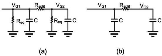
Figure 7.
Small-signal equivalent circuit diagram associated with in SMPS when split factor . (a) presents the equivalent resistance of and . (b) Ignored transistor-equivalent resistance.
Note that the small-signal equivalent circuit of the is not shown in the figure, because the change in the bias voltage is the main concern. is the equivalent resistance of and , and C is the equivalent capacitance of and each transistor combined.
When the drain of is injected with the same SET model as in Section 2, the current generated by the SET will cause voltage fluctuation at . Then, the voltage fluctuation at , is
is short for .
It can be seen that SET-induced voltage fluctuation at can be significantly reduced by splitting the transistor and by adding the resistor, reducing the fluctuation of .
If the value of is set to be small, the equation can be simplified to
This is the same as the equation in Figure 7b, so we use the simplified circuit shown in Figure 7b in the following analysis.
If we split the circuit into four parts (when split factor ), the voltage fluctuation of each stage is gradually reduced. Figure 8 shows the equivalent circuit when .
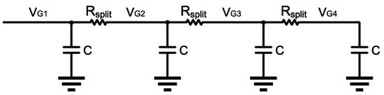
Figure 8.
Small-signal-equivalent circuit diagram associated with in SMPS when split factor .
In Figure 8, with the same voltage fluctuation at , the voltage fluctuation at is
The voltage change at is
The voltage change at is
The equations indicate that the voltage fluctuation is related to the value of the resistance . Furthermore, the more splits there are in SMPS, the smaller the corresponding bias voltage fluctuation of will be. Hence, the tail current change caused by the voltage fluctuation will be reduced and the total change in the current induced by SET will be smaller.
Next, we will compare the hardening effect of different splits and different values.
3.3. Simulations
As mentioned above, the number of splits is limited by the size of the transistors. In our original unhardened design, the size of and is 2 , . The size of is nm, . The size of and is nm, . In an SMPS circuit, and can be split into eight parts at most. We analyzed the performance when , , and in the following analysis.
To measure the hardening effect, the same double exponential current source with a peak value of 2 mA and a decay time of 2 ns was injected into the drain of to simulate the single particle hit. We simulate the total current sum of to in the SMPS circuit, as well as the frequency of the VCO output signal, considering how they change under the impaction of the same SET as the unhardened circuit.
Figure 9 illustrates the transient simulation results of the SMPS circuit when the split factor is 2.
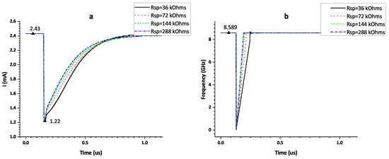
Figure 9.
SET-induced disturbance in (a) total current sum of and ; (b) VCO oscillation frequency with SMPS circuit when the split factor is 2.
It can be seen that in the increase in the resistance value of the split resistor, the change in the total current inducted by the SET becomes smaller and the stopping time is shortened. However, even if the resistance value reaches 288 , the total current of decreased from mA to mA when particle strike occurred, which is not enough for the EA to operate correctly. So it still cannot be fully immune to SET and will cause VCO oscillation to stop. The hardening effect is not obvious when in SMPS design.
Figure 10 presents the transient simulation results of a hardened circuit when the split factor is four.
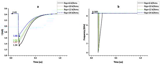
Figure 10.
SET induced disturbance in (a) total current sum of , , and . (b) VCO oscillation frequency with SMPS circuit when the split factor is 4.
As the resistance value of the split resistor increasing, the change in the total current due to SET becomes smaller. When the resistance value reaches 24 , the total current of decreases from mA to mA, no VCO oscillating stop occurs, and it can fully realize the immunity to SET. For our original unhardened design, the minimum split factor for effective hardening is when .
Figure 11 shows the transient simulation results of SMPS circuit when is split into eight parts.
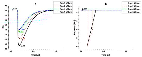
Figure 11.
SET induced disturbance in (a) total current sum of ~. (b) VCO oscillation frequency with SMPS circuit when the split factor is 8.
When the split factor , SET immunity can be achieved with a or split resistor. The total current of decreases from mA to mA and mA, respectively.
From Figure 9, Figure 10 and Figure 11, we can figure out that both the split factor and the resistance value affect the hardening effect of the SMPS circuit. Notably, a higher split factor requires more resistors. So we should compare the hardened effect in terms of total resistance value.
We consider the total resistance value needed for the hardening of . Naturally, the resistance value needed for the overall circuit should be multiplied by two because the overall hardened structure is symmetric.
Figure 12 illustrates the relation between the total resistance in the SMPS structure for hardening and the VCO oscillating recovery time at different split factors. The VCO oscillating recovery time’s decreasing trend for (black square in the figure) clearly shows that it is unlikely to achieve SET immunity. When the total resistance reaches about 40 with and , VCO oscillating does not stop when SET occurs.
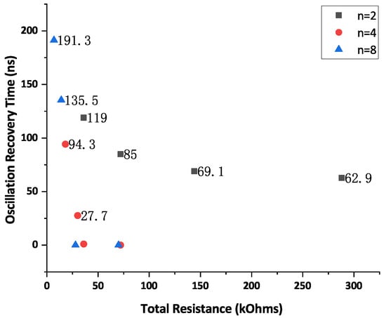
Figure 12.
VCO oscillating recovery time versus total resistance at different split factors.
Figure 13 presents the SET induced LDO output disturbance with different SMPS configurations. The voltage variation is less than 40 mV, while it is 207 mV in unhardened LDO (see Figure 3a).
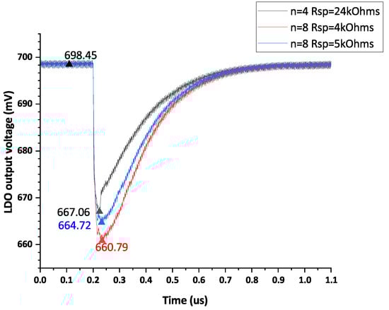
Figure 13.
SET induced LDO output disturbance with different SMPS configurations.
For the three combinations that can achieve the SET immunity, we simulated their power consumption. The power consumption here is the average power loss when the circuit is in a stable condition without SET. It is calculated by multiplying the power supply voltage of the LDO by the power supply current of the LDO. The result is shown in Table 1.

Table 1.
Power loss comparison.
In the simulation, SMPS does not increase power consumption because no extra transistors are added. Furthermore, the added resistors at both ends do not add much power because the circuit structure is symmetrical when the layout is matched.
Figure 14 illustrates an LDO PSRR comparison between unhardened LDO and several SMPS LDOs with different configurations. SMPS structure does not affect the PSRR of the LDO.
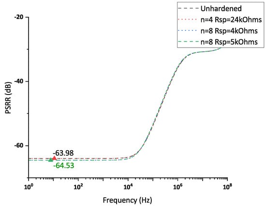
Figure 14.
LDO power-supply rejection ratio (PSRR) comparison.
The characteristics of SMPS are summarized and compared with other state-of-art techniques in Table 2.
Table 2.
Comparison with other state-of-the-art analog single-event transient (ASET) mitigation methods.
4. Conclusions
This paper analyzes the single-event transient (SET) sensitive nodes in a low-dropout regulator for an LC voltage-controlled oscillator. A symmetrical multi-path-splitting (SMPS) hardening structure for SET mitigation in LDO is proposed. Based on commercial 28 nm CMOS technology, the Spice simulation results indicate that SMPS reduces 80.8% of SET-induced LDO output fluctuation. This structure has no additional power consumption and does not effect the LDO power-supply rejection ratio.
Author Contributions
Conceptualization, X.C. and Q.G.; methodology, X.C. and Q.G.; validation, X.C.; formal analysis, X.C.; investigation, X.C.; writing, X.C.; visualization and supervision, Y.G.; funding acquisition, Y.G. and H.Y. All authors have read and agreed to the published version of the manuscript.
Funding
This research was funded by National Natural Science Foundation of China, grant number 61772540, 62104257; National University of Defense Technology Pre-research foundation, grant number ZK21-34; National Defense Science and Technology Key Laboratory fund, grant number WDZC20215250110.
Institutional Review Board Statement
Not applicable.
Informed Consent Statement
Not applicable.
Data Availability Statement
The data presented in this article can be obtained from the corresponding author upon reasonable request.
Conflicts of Interest
The authors declare no conflict of interest.
Abbreviations
The following abbreviations are used in this manuscript:
| ASET | analog single-event transient |
| CP | charge pump |
| DC | direct current |
| DIV | frequency divider |
| EA | error amplifier |
| LDO | low-dropout regulator |
| LPF | low-pass filter |
| PLL | phase-locked loop |
| PSRR | power-supply rejection ratio |
| RH | radiation-hardened |
| RHBD | radiation-hardened-by-design |
| RHBP | radiation-hardened-by-process |
| VCO | voltage-controlled oscillator |
| SEE | single-event effect |
| SET | single-event transient |
| SEU | single-event upset |
| SMPS | symmetrical multi-path splitting |
| TMD | three-mode redundancy |
References
- Chung, H.H.; Chen, W.; Bakkaloglu, B.; Barnaby, H.J.; Vermeire, B.; Kiaei, S. Analysis of Single Events Effects on Monolithic PLL Frequency Synthesizers. IEEE Trans. Nucl. Sci. 2006, 53, 3539–3543. [Google Scholar] [CrossRef]
- Boulghassoul, Y.; Massengill, L.W.; Sternberg, A.L.; Bhuva, B.L. Effects of technology scaling on the SET sensitivity of RF CMOS Voltage-controlled oscillators. IEEE Trans. Nucl. Sci. 2005, 52, 2426–2432. [Google Scholar] [CrossRef]
- Hubert, G.; Truyen, D.; Artola, L.; Briet, M.; Heng, C.; Lakys, Y.; Leduc, E. SET and SEU Analyses Based on Experiments and Multi-Physics Modeling Applied to the ATMEL CMOS Library in 180 and 90-nm Technological Nodes. IEEE Trans. Nucl. Sci. 2014, 61, 3178–3186. [Google Scholar] [CrossRef]
- Kroupa, V.F. Noise Properties of PLL Systems. IEEE Trans. Commun. 1982, 30, 2244–2252. [Google Scholar] [CrossRef]
- Gui, X.; Tang, B.; Tang, R.; Li, D.; Geng, L. Low-Supply Sensitivity LC VCOs with Complementary Varactors. IEEE Trans. Very Large Scale Integr. (VLSI) Syst. 2020, 28, 1589–1599. [Google Scholar] [CrossRef]
- Chen, J.; Zhang, W.; Sun, Q.; Liu, L. An 8–12.5-GHz LC PLL with Dual VCO and Noise-Reduced LDO Regulator for Multilane Multiprotocol SerDes in 28-nm CMOS Technology. Electronics 2021, 10, 1686. [Google Scholar] [CrossRef]
- Lin, T.-H.; Hsu, R.-L.; Li, C.-L.; Tseng, Y.-C. A 5 GHz, 192.6 dBc/Hz/mW FOM, LC–VCO System with Amplitude Control Loop and LDO Voltage Regulator in 0.18 μm CMOS. IEEE Microw. Wirel. Compon. Lett. 2007, 17, 730–732. [Google Scholar] [CrossRef]
- Prinzie, J.; Christiansen, J.; Moreira, P.; Steyaert, M.; Leroux, P. Comparison of a 65 nm CMOS Ring- and LC-Oscillator Based PLL in Terms of TID and SEU Sensitivity. IEEE Trans. Nucl. Sci. 2017, 64, 245–252. [Google Scholar] [CrossRef]
- Biereigel, S.; Kulis, S.; Leroux, P.; Moreira, P.; Kolpin, A.; Prinzie, J. Single-Event Effect Responses of Integrated Planar Inductors in 65-nm CMOS. IEEE Trans. Nucl. Sci. 2021, 68, 2587–2597. [Google Scholar] [CrossRef]
- Prinzie, J.; De Smedt, V. Time-Dependent Single-Event Effects in CMOS LC-Oscillators. IEEE Trans. Nucl. Sci. 2019, 66, 2048–2054. [Google Scholar] [CrossRef]
- Jagtap, S.; Anmadwar, S.; Rudrapati, S.; Gupta, S. A Single-Event Transient-Tolerant High-Frequency CMOS Quadrature Phase Oscillator. IEEE Trans. Nucl. Sci. 2019, 66, 2072–2079. [Google Scholar] [CrossRef]
- Wang, T.; Wang, K.; Chen, L.; Dinh, A.; Bhuva, B.; Shuler, R. A RHBD LC-Tank Oscillator Design Tolerant to Single-Event Transients. IEEE Trans. Nucl. Sci. 2010, 57, 3620–3625. [Google Scholar] [CrossRef]
- Karthigeyan, K.A.; Radha, S. Single event transient study on PMOS-NMOS cross-coupled LC-VCO using PLL. Int. J. Electron. 2020, 108, 378–394. [Google Scholar] [CrossRef]
- Zhang, Z.; Djahanshahi, H.; Gu, C.; Patel, M.; Chen, L. Single-Event Effects Characterization of LC-VCO PLLs in a 28-nm CMOS Technology. IEEE Trans. Nucl. Sci. 2020, 67, 2042–2050. [Google Scholar] [CrossRef]
- Chen, W.; Varanasi, N.; Pouget, V.; Barnaby, H.J.; Vermeire, B.; Adell, P.C.; Copani, T.; Fouillat, P. Impact of VCO Topology on SET Induced Frequency Response. IEEE Trans. Nucl. Sci. 2007, 54, 2500–2505. [Google Scholar] [CrossRef]
- Johnston, A.H.; Miyahira, T.F.; Irom, F.; Laird, J.S. Single-Event Transients in Voltage Regulators. IEEE Trans. Nucl. Sci. 2006, 53, 3455–3461. [Google Scholar] [CrossRef]
- Najafizadeh, L.; Phillips, S.D.; Moen, K.A.; Diestelhorst, R.M.; Bellini, M.; Saha, P.K.; Cressler, J.D.; Vizkelethy, G.; Turowski, M.; Raman, A.; et al. Single Event Transient Response of SiGe Voltage References and Its Impact on the Performance of Analog and Mixed-Signal Circuits. IEEE Trans. Nucl. Sci. 2009, 56, 3469–3476. [Google Scholar] [CrossRef]
- Allen, G.R.; Adell, P.C.; Dakai, C.; Musil, P. Single-Event Transient Testing of Low Dropout PNP Series Linear Voltage Regulators. IEEE Trans. Nucl. Sci. 2012, 59, 2764–2771. [Google Scholar] [CrossRef]
- Irom, F.; Miyahira, T.F.; Adell, P.C.; Laird, J.S.; Conder, B.; Pouget, V.; Essely, F. Investigation of Single-Event Transients in Linear Voltage Regulators. IEEE Trans. Nucl. Sci. 2008, 55, 3352–3359. [Google Scholar] [CrossRef]
- Zhao, Q.; Yang, G.; Sun, Y.; Yu, P.; Chen, J.; Liang, B. Research on the effect of single-event transient of an on-chip linear voltage regulator fabricated on 130 nm commercial CMOS technology. Microelectron. Reliab. 2017, 73, 116–121. [Google Scholar] [CrossRef]
- Chen, Z.; Lin, M.; Ding, D.; Zheng, Y.; Sang, Z.; Zou, S. Analysis of Single-Event Effects in a Radiation-Hardened Low-Jitter PLL Under Heavy Ion and Pulsed Laser Irradiation. IEEE Trans. Nucl. Sci. 2017, 64, 106–112. [Google Scholar] [CrossRef]
- Yuan, H.; Chen, J.; Liang, B.; Guo, Y. Fault-tolerant multi-node coupling triple mode redundancy voltage controlled oscillator for reducing soft error in clock and data recovery. Electron. Lett. 2019, 55, 250–252. [Google Scholar] [CrossRef]
- Duan, Z.; Ding, Y.; Lu, C.; Zhao, Z.; Hu, J.; Tan, H. A single-event transient hardened LDO regulator with built-in filter. IEICE Electron. Express 2015, 12, 20150850. [Google Scholar] [CrossRef][Green Version]
- Fan, H.; Feng, L.; Cen, Y.; Fang, Z.; Li, Y.; Qi, X.; Feng, Q.; Gatti, U.; Wei, Q.; Heidari, H. Fast-Transient Radiation-Hardened Low-Dropout Voltage Regulator for Space Applications. IEEE Trans. Nucl. Sci. 2021, 68, 1094–1102. [Google Scholar] [CrossRef]
- Lapuyade, H.; Mazouffre, O.; Goumballa, B.; Pignol, M.; Malou, F.; Neveu, C.; Pouget, V.; Deval, Y.; Begueret, J.B. A Heavy-Ion Tolerant Clock and Data Recovery Circuit for Satellite Embedded High-Speed Data Links. IEEE Trans. Nucl. Sci. 2007, 54, 2080–2085. [Google Scholar] [CrossRef]
- Guo, Q.; Guo, Y.; Liang, B.; Chen, J.; Chen, X. A soft-error-tolerant, 1.25 GHz to 3.125 GHz, 3.18 ps RMS-jitter CPPLL in 40 nm CMOS process. Microelectron. Reliab. 2021, 124, 114337. [Google Scholar] [CrossRef]
- Wang, L.; Han, X.; Zhao, Y.; Bian, Q.; Yue, S.; Lu, S.; Shu, L.; Liu, J.; Li, T. Single-Event Transient Analysis and Hardening in a 180 nm CMOS Embedded Low-Dropout Regulator. In Proceedings of the 2017 17th European Conference on Radiation and Its Effects on Components and Systems (RADECS), Geneva, Switzerland, 2–6 October 2017. [Google Scholar] [CrossRef]
- Wang, X.; Bakkaloglu, B. Systematic Design of Supply Regulated LC-Tank Voltage-Controlled Oscillators. IEEE Trans. Circuits Syst. I Reg. Pap. 2008, 55, 1834–1844. [Google Scholar] [CrossRef]
- Razavi, B. Jitter-Power Trade-Offs in PLLs. IEEE Trans. Circuits Syst. I Reg. Pap. 2021, 68, 1381–1387. [Google Scholar] [CrossRef]
- Black, D.A.; Robinson, W.H.; Wilcox, I.Z.; Limbrick, D.B.; Black, J.D. Modeling of Single Event Transients with Dual Double-Exponential Current Sources: Implications for Logic Cell Characterization. IEEE Trans. Nucl. Sci. 2015, 62, 1540–1549. [Google Scholar] [CrossRef]
- Liu, J.; Sun, Q.; Liang, B.; Chen, J.; Chi, Y.; Guo, Y. Bulk Bias as an Analog Single-Event Transient Mitigation Technique with Negligible Penalty. Electronics 2019, 9, 27. [Google Scholar] [CrossRef]
Publisher’s Note: MDPI stays neutral with regard to jurisdictional claims in published maps and institutional affiliations. |
© 2022 by the authors. Licensee MDPI, Basel, Switzerland. This article is an open access article distributed under the terms and conditions of the Creative Commons Attribution (CC BY) license (https://creativecommons.org/licenses/by/4.0/).