Abstract
The NdNiO3 (NNO) system has attracted a considerable amount of attention owing to the discovery of superconductivity in Nd0.8Sr0.2NiO2. In rare-earth nickelates, Ruddlesden–Popper (RP) faults play a significant role in functional properties, motivating our exploration of its microstructural characteristics and the electronic structure. Here, we employed aberration-corrected scanning transmission electron microscopy and spectroscopy to study a NdNiO3 film grown by layer-by-layer molecular beam epitaxy (MBE). We found RP faults with multiple configurations in high-angle annular dark-field images. Elemental intermixing occurs at the SrTiO3–NdNiO3 interface and in the RP fault regions. Quantitative analysis of the variation in lattice constants indicates that large strains exist around the substrate–film interface. We demonstrate that the Ni valence change around RP faults is related to a strain and structure variation. This work provides insights into the microstructure and electronic-structure modifications around RP faults in nickelates.
1. Introduction
The recent discovery of nickel-based superconductors has filled the gap in nickel-based oxide materials in superconducting systems [1,2,3,4,5]. The infinite-layer phase NdNiO2 can only be synthesized from the precursor ABO3 perovskite structure by removing apical oxygen atoms from NiO6 octahedra through soft-chemistry topotactical reduction [6]. For stabilization of the superconducting phase, chemical doping with divalent Sr replacing trivalent Nd is crucial. Optimal doping with the highest superconducting transition temperature (around 15 K) has been found in Nd0.8Sr0.2NiO2 thin films [1]. During pulsed-laser deposition growth of Sr-doped thin NdNiO3 films, a strong tendency to form Ruddlesden–Popper (RP) faults has been reported [2]. In addition, the epitaxial strain from the substrate can induce the formation of RP faults [7,8]. These RP faults display an atomic structure, where the inclusion of an additional AO layer breaks the long-range order of the ABO3 perovskite phase [3,7,8,9,10,11,12,13,14,15,16,17]. As the microstructure of the entire film determines its electric properties, investigation of the defect structure and associated variations in the local electronic structure in nickelates is indispensable. Moreover, RP structures are related to a variety of physical and chemical properties, e.g., electro-catalytic activities [11], microwave dielectric performance [18], magnetic properties [19], and ferroelectric properties [20].
Epitaxial strain and/or a cation non-stoichiometry, e.g., an excess of A or B in the ABO3 structure, can induce the generation of different RP faults that consist of an intergrowth of rock-salt-type and perovskite-type building blocks [11,12,21,22]. A single rock-salt layer can be described as an a/2 <111> or a/2 <110> stacking fault displaying a zigzag arrangement of cations [17]. The (AO)(ABO3)n RP structure forms when a rock-salt layer separates the n-layered structure of n(ABO3) [9,23,24]. Detemple et al. [13] reported on three-dimensionally arranged RP faults in LaNiO3–LaAlO3 superlattices, where the authors observed an identical contrast of A and B columns in the ABO3 structure in high-angle annular dark-field (HAADF) scanning transmission electron microscopy (STEM) investigations. Coll et al. [23] identified multiple configurations of RP faults in a LaNiO3 film based on atomistic modeling, experimental HAADF-STEM investigations, and HAADF-image simulations. Bak et al. [11] demonstrated a strong tetragonal Jahn–Teller distortion of the RP-fault plane in LaNiO3, proving a correlation between the octahedral distortion and the electro-catalytic performance of La-based perovskite oxides. However, to the best of our knowledge, influences of different RP-fault types on the variation in the electronic structure and especially in the Ni valence state have not been reported so far for NNO thin films.
Here, we characterize the local atomic structure of different RP-fault configurations and focus on the electronic properties around RP faults in the NNO film, based on advanced aberration-corrected scanning transmission electron microscopy (STEM) and electron energy-loss spectroscopy (EELS). RP-fault formation starts after a critical thickness of around two unit cells above the substrate–film interface, where different RP-fault types are found to be inhomogeneously distributed in the entire film. We identify an elemental intermixing in various RP-fault regions with different structural configurations. In addition, we demonstrate that the variation in the Ni oxidation state around different RP faults relates to the alteration of the chemical composition, possibly triggered by epitaxial strain.
2. Materials and Methods
The NdNiO3 film was grown on a SrTiO3 (001) single-crystal substrate at 630 °C in an ozone–oxygen atmosphere with a pressure of 1.8 × 10⁻⁵ Torr in an atomic layer-by-layer fashion in a custom-made ozone-assisted MBE setup. Then, it was cooled down after the growth in the same atmosphere. The fluxes of the effusion cells were calibrated prior to growth with a quartz crystal microbalance and monitored during growth by in situ reflection high-energy electron diffraction.
The TEM sample was prepared by automated tripod polishing (in an Allied MultiPrep System) until the sample was thinner than ~15 μm, after which Ar-ion milling at liquid N2 temperature was performed by an ion polishing system (PIPS, Gatan, model 691) [25]. The milling step was performed at a voltage of 0.5 kV to reduce the damage to the surface of the sample. We used a spherical-aberration-corrected microscope (JEOL JEM-ARM200F, JEOL Co., Ltd., Tokyo, Japan) equipped with a DCOR probe corrector (CEOS GmbH, Heidelberg, Germany) and a Gatan GIF Quantum ERS with a Gatan K2 camera at 200 kV to acquire STEM images and EELS spectra. The convergence angle was set to 20.4 mrad and the collection semi-angles for high-angle annular dark-field (HAADF) imaging and annular bright-field (ABF) imaging were set to 70–300 mrad and 10–20 mrad, respectively. The EELS spectra were acquired at a dispersion of 0.5 eV per channel (with an energy resolution of ~1 eV). The principal component analysis (PCA) method [26] was utilized to optimize the signal and to reduce the noise in the EELS maps.
3. Results and Discussion
As the overview HAADF image in Figure 1a shows, the film thickness is around 9 nm, in good agreement with the X-ray reflectometry, and a large number of RP faults are distributed randomly throughout the entire film. The critical thickness for RP-fault formation is around two to three unit cells. In this range, the film grows coherently with the substrate. Similar observations were also made and are discussed in [2]. Above the critical thickness, defects are introduced to accommodate the strain. We note that this growth mode resembles the Stranski–Krastanov mode; however, it differs from it by not forming islands on the coherent NNO layer, but instead forming a continuous film. According to the relationship that the atomic-column brightness is approximately proportional to Z1.7 (Z: atomic number), the sufficient contrast difference enables us to distinguish the atomic columns [27]. For example, we can observe a sharp interface between STO and NNO. A high density of irregularly distributed RP faults forms generally three unit cells away from the substrate.
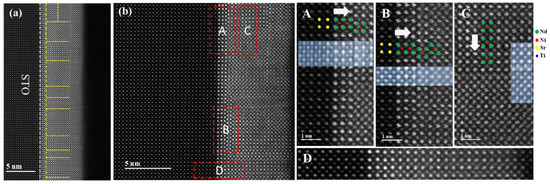
Figure 1.
(a) An overview HAADF image of a NdNiO3 film grown on a (001) SrTiO3 single-crystal substrate. (b) Enlarged image showing different types of RP faults and fault-free regions marked by red dashed boxes in the NdNiO3 layer: (A) a/2 <111> shift; (B) single intergrowth layer of {NdNiO3}; (C) identical contrast of A/B sites in NdNiO3; (D) fault-free region. The contrast-inverted ABF images (shaded regions) show the oxygen columns around the RP faults.
Although we cannot exclude non-stoichiometry during film growth as a reason for RP-fault formation, a major driving force in our system is the reduction in the lattice mismatch between STO (3.905 Å) and NNO (pseudocubic lattice constant: 3.807 Å) as we do not observe any misfit dislocation that could alternatively have reduced the strain. In the enlarged HAADF image (Figure 1b), several configurations of RP faults in the NNO layer are marked with red dashed boxes (A, B, and C, respectively). The apparent a/2<110> shift for RP fault A, where a is the lattice constant of the pseudocubic unit cell, is likely to be the component of the true displacement vector a/2<111> projected along the beam direction [24]. RP fault B shows a single intergrowth layer of {NdNiO3}, forming a typical ‘214’ structure of the RP phase (Nd2NiO4) by combining a rock-salt-type layer and a perovskite-type layer. In the case of RP fault C, the contrast difference between the A and B sites in NNO disappears due to the overlap of the A and B columns along the viewing direction. [13,23]. Additionally, the red dashed box D marks a fault-free region displaying a perovskite structure of the NNO layer.
Furthermore, we can observe the oxygen columns from the inverted ABF images (shaded in Figure 1) around the edges of these RP faults. The slight elongation of Ni–O bonds along the z-axis at the plane of RP fault A is apparent (see also Figure S2b), which can result in a significant splitting of the eg level of the Ni 3d orbital and a relative variation in the O 2p level based on the Jahn–Teller effect [11]. From a layer-by-layer structural perspective [11], the distortion of oxygen anions toward the fault plane can reduce the strong repulsion between two [NdO]+ layers and achieve an energetically favorable structure. Around RP fault B, the elongation of Ni–O bonds is not clear, accompanying a visible distortion of [NiO6] octahedra (see Figure S3). The reduced contrast of oxygen columns is possibly due to the existence of oxygen vacancies. Additionally, we observe distinct oxygen columns at RP fault C without apparent changes in the oxygen structure. Owing to the overlapping of elements around the edge of RP fault C, we observe a homogeneous distribution of oxygen.
To investigate the effects of RP faults on the electronic character of the NNO film, we performed STEM-EELS measurements with atomic resolution. Figure 2a,d show the HAADF images of RP faults A and B, respectively. For the sake of improving the signal-to-noise ratio, the O-K and Ni-L2,3 edges were extracted from the red dashed boxes with a width of one unit cell shown in Figure 2b,e. From the NdNiO3 reference, we observe a strong pre-peak A at the O K edge, which is associated with the hybridization of O 2p and Ni 3d orbitals, reflecting the covalency of Ni–O bonding and the oxidation state of Ni [28,29]. The pre-peak of the O K edge is weak or even absent around the RP faults, which is related to the changes in the local Ni–O distances due to epitaxial strain and RP faults [28,30]. In addition, the strong Nd–O interaction in the rock-salt layer results in a distinct shoulder of peak C. Close to the STO–NNO interface, the intermixing of Ti into Ni causes the appearance of peak B that arises from the Ti 3d–O 2p hybridized states. Peak B almost disappears in cells 4–7. Peak C corresponds to the O 2p states hybridized with Sr 4d in STO or Nd 5d in NNO. Peak D is due to the O 2p states hybridized with Ni 4 sp and Nd 5p states [31]. The L3 and L2 peaks of Ni arise from excitation of electrons from the 2p3/2 and 2p1/2 core levels to the unoccupied 3d band, which is used to determine the valence state of the transition metal from the white-line ratio and chemical shift [28]. The slight variations in peak positions and crystal-field splitting observed in Figure 2b,e imply changes in the electronic structure of Ni for both types of RP faults. We quantified the white-line ratio, which is shown in Figure 2c,f. From the DigitalMicrograph database [32], we calculated the Ni3+ and Ni2+ references, which are expected to correspond to the fault-free NdNiO3 and NiO films. These are shown as black and blue dashed lines in Figure 2c,f, respectively. We observe that the L3/L2 ratio increases near RP-fault planes and in the fault-free NNO layers close to the STO substrate, suggesting a decreased valence of Ni. In the fault-free NNO layer (the seventh unit cell) far from the fault planes, the valence of Ni is close to 3+, as expected. The Ni L3/L2 intensity ratio in RP fault B is a little higher than that in RP fault A, indicating a lower valence of Ni around RP fault B.
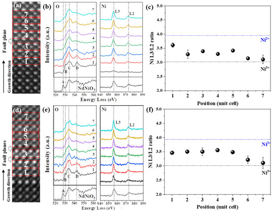
Figure 2.
The HAADF images of (a) RP fault A and (d) RP fault B used for EELS data acquisition. Atomic layers are numbered from 1 to 7 (b,e) O K and Ni L spectra extracted from the red dashed boxes in the HAADF images of RP faults A and B, respectively. Spectral features are marked by letters A–D (c,f) The calculated Ni L3/L2 white-line intensity ratio around RP fault A and RP fault B, respectively. The Ni3+ and Ni2+ references are from NdNiO3 and NiO, respectively. The error bar was obtained by measuring different regions.
The atomically resolved EELS maps shown in Figure 3 confirm the atomic arrangement around RP faults A and B. The distribution of cations from the color-coded EELS maps indicates elemental intermixing at the STO–NNO interface. In the RP fault regions, the zigzag arrangement of the Nd atoms and additional intergrowth of an NNO layer verify the atomic structures visible in ADF images. Figure 3a shows the EELS maps of RP fault A, where Ni and Nd columns can be clearly distinguished. In the RP fault B region (Figure 3b), a small amount of Ni is intermixed into Nd columns. Owing to the random distribution of RP faults, it is possible that the observed Nd/Ni signal intermixing arises from the partial overlapping of Ni and Nd. Similarly, the obvious intermixing of Ni and Nd signals at RP fault C shown in Figure S1a is due to the Ni/Nd overlapping, explaining why Ni and Nd columns display the same contrast in ADF images. Moreover, the Ni L2,3 and O K edges extracted from fault-free and Ni/Nd overlapping regions show the same shapes and peak positions. The pronounced small pre-peak of the O K edge is consistent with the Ni3+ reference in Figure 2b,e.
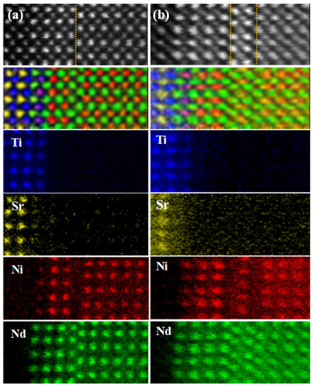
Figure 3.
HAADF images of RP fault A (a) and RP fault B (b). Color-coded elemental maps of Ti (blue), Sr (yellow), Ni (red), and Nd (green) determined from an EELS spectrum image. The RP fault planes are marked with yellow dashed lines. The EELS spectra are shown in Figure S4.
In order to explore the potential mechanism of the valence change in Ni, we quantitatively analyzed the variation in the lattice constant around RP faults A and B. As the lattice constant of STO is a little larger than that of NNO, an in-plane tensile strain of ~2.5% is induced in the NNO film. From Figure 4a,b, the critical thickness of the NNO layer is two unit cells. By calculating the Nd–Nd distance across the STO–NNO interface and across the RP fault plane from the HAADF images, we found that the in-plane tensile strain is maintained at ~2.5% for the first two unit cells before the formation of RP faults. The in-plane Nd–Nd distance decreases to 3.85 ± 0.04 Å at the fault-free layers far from the RP fault plane shown in Figure 4c,d. According to theoretical calculations, the O stoichiometry in NNO is sensitive to the in-plane tensile strain [33]. The formation energy of an oxygen vacancy becomes negative when the in-plane tensile strain is higher than 1.9% [33]. Therefore, the probability for the generation of oxygen vacancies close to the interface is higher than that in fault-free layers where the in-plane strain is significantly released. In addition, oxygen vacancies are more easily generated in the NiO2 plane as their formation energy in the NiO2 plane is about 1.7 eV lower than in the NdO plane under a tensile strain [33]. From the inverted ABF image in Figure S2, we can clearly observe that the contrast of oxygen columns in the NiO2 planes (marked with white arrows) is smaller than that in the NdO planes (marked with orange arrows), indicative of the possible existence of oxygen vacancies in our sample. Thus, the strain-induced oxygen vacancies in the region close to the STO–NNO interface can result in a decrease in the Ni valence. In addition, the sharp drop of the out-of-plane Nd–Nd distance to ~3.5 Å observed a few atomic columns away from the fault plane suggests a large out-of-plane contraction, which gradually increases to ~3.8 Å across the fault-plane and into the fault-free region as shown in Figure 4c,d. Therefore, the generation of RP faults effectively relaxes the epitaxial strain from the substrate, which is consistent with the previous report [12].
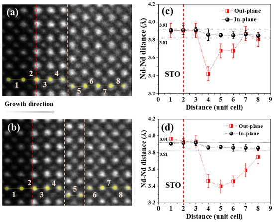
Figure 4.
(a,b) HAADF images of RP fault A and B, respectively, used for the quantitative analysis of Nd–Nd distances. The numbers indicate the positions of unit cells. (c,d) The Nd–Nd distances along in-plane and out-of-plane directions across RP fault A and B, respectively. The red dashed lines indicate the STO–NNO interface. The orange dashed lines mark the fault planes.
It is worth mentioning that the average oxidation state of nickel varies between 2+ and 3+ for different n in the RP structure (Ndn+1NinO3n+1). In principle, Ni is divalent in the ‘214’ end member of the RP structure (Nd2NiO4), where the [NdO]+ layer donates an additional electron for the NNO layer [34]. However, the measured Ni valence in RP fault B shows a mixed valence between 2+ and 3+. The RP fault B structure is similar to the Nd2NiO4 structure, but the [NdO]+ layer is shared by adjacent NNO layers. We can observe the irregular distribution of different types of RP faults and fault-free NNO layers in Figure 1b. As mentioned above, at the NNO layer close to the substrate, the tensile strain can induce the formation of oxygen vacancies, which means that the additional electron can be partially compensated for by oxygen vacancies in the adjacent NNO layer. Thus, the Ni valence can be higher than 2+ in the intergrowth layer of NNO. Given that the Ni/Nd signal intermixing occurs at the intergrowth layer of NNO, it is possible that the measured Ni signal partially arises from the fault-free NNO layer, which can also lead to a mixed Ni valence in RP fault B. In terms of RP fault A, there is no obvious elemental intermixing and Ni ions show a higher valence (closer to 3+) than in RP fault B. The variation in the Ni oxidation state is mainly ascribed to the additional NdO layer and the possible oxygen vacancies.
4. Conclusions
Based on STEM and EELS measurements, we systematically studied the atomic structure of RP faults and the effects of RP faults on the local electronic configuration of Ni in a NdNiO3 film. Several RP faults were detected, showing, e.g., a/2<111> shifts, intergrowth layers of NdNiO3, and overlapping Nd and Ni columns. The critical thickness for RP fault formation is around two unit cells and no misfit dislocations are visible. The generation of a high density of RP faults effectively relaxes the epitaxial strain from the substrate. We observed the elongation and distortion of the oxygen sublattice around RP-fault planes, which is theoretically beneficial to reduce the strong repulsion between two neighboring [NdO]+ layers. We analyzed the variation in the Ni oxidation state around RP faults in NNO. The changed valence of Ni around RP-fault planes is mainly associated with the variations in the strain and atomic structure. On the one side, the tensile strain might induce oxygen vacancies at the fault-free layer of NdNiO3 close to the substrate. On the other side, the additional [NdO]+ layer can lead to a reduction in the valence of Ni in RP fault regions. This work highlights how the distribution of strain and atomic structure changes around RP faults lead to a spatially varying electronic configuration in NdNiO3.
Supplementary Materials
The following supporting information can be downloaded at: https://www.mdpi.com/article/10.3390/sym14030464/s1. Figure S1. (a) HAADF image of RP fault C and corresponding EELS maps of Ni (red) and Nd (green). (b) Ni L edge and (c) O K edge extracted from regions marked by red dashed boxes in the HAADF image. Figure S2. (a) HAADF and (b) inverted ABF images of RP fault A. The white arrows indicate basal O, and orange arrows represent apical O. Ni columns are marked by red circles. Figure S3. (a) HAADF and (b) inverted ABF image of RP fault B. The yellow circles indicate O columns, and red spots mark the Ni columns. White and green arrows indicate the fault planes. Figure S4. (a) HAADF image used for EELS data acquisition. (b,c) EELS spectra extracted from the red dashed boxes in the HAADF image.
Author Contributions
Methodology, C.Y., D.P., R.A.O. and G.L.; formal analysis, C.Y., H.W.; resources, B.K. and P.A.v.A.; writing—original draft, C.Y.; writing—review and editing, W.S., H.W., E.B. and P.A.v.A.; supervision, Y.W., W.S. and P.A.v.A. All authors have read and agreed to the published version of the manuscript.
Funding
The authors acknowledge the funding support from the European Union’s Horizon 2020 research and innovation program under Grant Agreement No. 823717-ESTEEM3 and the Deutsche Forschungsgemeinschaft (DFG, German Research Foundation) TRR 80-project G1.
Institutional Review Board Statement
Not applicable.
Informed Consent Statement
Not applicable.
Data Availability Statement
The datasets generated during and/or analysed during the current study are available from the corresponding author on reasonable request.
Acknowledgments
We are thankful to U. Salzberger for the TEM sample preparation and K. Hahn and P. Kopold for the help with the TEM.
Conflicts of Interest
The authors declare no conflict of interest.
References
- Li, D.; Lee, K.; Wang, B.Y.; Osada, M.; Crossley, S.; Lee, H.R.; Cui, Y.; Hikita, Y.; Hwang, H.Y. Superconductivity in an infinite-layer nickelate. Nature 2019, 572, 624–627. [Google Scholar] [CrossRef] [PubMed]
- Lee, K.; Goodge, B.H.; Li, D.; Osada, M.; Wang, B.Y.; Cui, Y.; Kourkoutis, L.F.; Hwang, H.Y. Aspects of the synthesis of thin film superconducting infinite-layer nickelates. APL Mater. 2020, 8, 041107. [Google Scholar] [CrossRef] [Green Version]
- Li, D.; Wang, B.Y.; Lee, K.; Harvey, S.P.; Osada, M.; Goodge, B.H.; Kourkoutis, L.F.; Hwang, H.Y. Superconducting Dome in Nd1−xSrxNiO2 Infinite Layer Films. Phys. Rev. Lett. 2020, 125, 027001. [Google Scholar] [CrossRef] [PubMed]
- Hepting, M.; Li, D.; Jia, C.J.; Lu, H.; Paris, E.; Tseng, Y.; Feng, X.; Osada, M.; Been, E.; Hikita, Y.; et al. Electronic structure of the parent compound of superconducting infinite-layer nickelates. Nat. Mater. 2020, 19, 381–385. [Google Scholar] [CrossRef] [PubMed]
- Goodge, B.H.; Li, D.; Lee, K.; Osada, M.; Wang, B.Y.; Sawatzky, G.A.; Hwang, H.Y.; Kourkoutis, L.F. Doping evolution of the Mott–Hubbard landscape in infinite-layer nickelates. Proc. Natl. Acad. Sci. USA 2021, 118, e2007683118. [Google Scholar] [CrossRef] [PubMed]
- Hayward, M.A.; Green, M.A.; Rosseinsky, M.J.; Sloan, J. Sodium Hydride as a Powerful Reducing Agent for Topotactic Oxide Deintercalation: Synthesis and Characterization of the Nickel(I) Oxide LaNiO2. J. Am. Chem. Soc. 1999, 121, 8843–8854. [Google Scholar] [CrossRef]
- Bak, J.; Chung, S.-Y. Observation of fault-free coherent layer during Ruddlesden-Popper faults generation in LaNiO3 thin films. J. Korean Ceram. Soc. 2020, 58, 169–177. [Google Scholar] [CrossRef]
- Qi, H.; Chen, X.; Wu, M.; Benckise, E.; Logvenov, G.; Christiani, G.; Keimer, B.; Kaiser, U. Formation mechanism of Ruddlesden-Popper faults in compressive-strained ABO3 perovskite superlattices. Nanoscale 2021, 13, 20663–20669. [Google Scholar] [CrossRef]
- Ruddlesden, S.N.; Popper, P. New compounds of the K2NIF4 type. Acta Crystallogr. 1957, 10, 538–539. [Google Scholar] [CrossRef]
- Yu, Y.; Zhang, D.; Yang, P. Ruddlesden-Popper Phase in Two-Dimensional Inorganic Halide Perovskites: A Plausible Model and the Supporting Observations. Nano Lett. 2017, 17, 5489–5494. [Google Scholar] [CrossRef] [Green Version]
- Bak, J.; Bin Bae, H.; Kim, J.; Oh, J.; Chung, S.-Y. Formation of Two-Dimensional Homologous Faults and Oxygen Electrocatalytic Activities in a Perovskite Nickelate. Nano Lett. 2017, 17, 3126–3132. [Google Scholar] [CrossRef] [PubMed]
- Bak, J.; Bin Bae, H.; Oh, C.; Son, J.; Chung, S.-Y. Effect of Lattice Strain on the Formation of Ruddlesden-Popper Faults in Heteroepitaxial LaNiO3 for Oxygen Evolution Electrocatalysis. J. Phys. Chem. Lett. 2020, 11, 7253–7260. [Google Scholar] [CrossRef] [PubMed]
- Detemple, E.; Ramasse, Q.M.; Sigle, W.; Cristiani, G.; Habermeier, H.U.; Keimer, B.; Van Aken, P.A. Ruddlesden-Popper faults in LaNiO3/LaAlO3 superlattices. J. Appl. Phys. 2012, 112, 013509. [Google Scholar] [CrossRef] [Green Version]
- Thind, A.S.; Luo, G.; Hachtel, J.A.; Morrell, M.V.; Cho, S.B.; Borisevich, A.Y.; Idrobo, J.; Xing, Y.; Mishra, R. Atomic Structure and Electrical Activity of Grain Boundaries and Ruddlesden-Popper Faults in Cesium Lead Bromide Perovskite. Adv. Mater. 2019, 31, e1805047. [Google Scholar] [CrossRef] [PubMed]
- Li, Z.; Guo, W.; Zhang, T.T.; Song, J.H.; Gao, T.Y.; Gu, Z.B.; Nie, Y.F. Epitaxial growth and electronic structure of Ruddlesden-Popper nickelates (Lan+1NinO3n+1, n = 1–5). APL Mater. 2020, 8, 091112. [Google Scholar] [CrossRef]
- Wang, W.Y.; Tang, Y.L.; Zhu, Y.L.; Suriyaprakash, J.; Xu, Y.-B.; Liu, Y.; Gao, B.; Cheong, S.-W.; Ma, X.L. Atomic mapping of Ruddlesden-Popper faults in transparent conducting BaSnO3-based thin films. Sci. Rep. 2015, 5, 16097. [Google Scholar] [CrossRef]
- Gauquelin, N.; Benckiser, E.; Kinyanjui, M.K.; Wu, M.; Lu, Y.; Christiani, G.; Logvenov, G.; Habermeier, H.U.; Kaiser, U.; Keimer, B.; et al. Atomically resolved EELS mapping of the interfacial structure of epitaxially strained LaNiO3/LaAlO3 superlattices. Phys. Rev. B 2014, 90, 195140. [Google Scholar] [CrossRef]
- Lee, C.-H.; Orloff, N.; Birol, T.; Zhu, Y.; Goian, V.; Rocas, E.; Haislmaier, R.; Vlahos, E.; Mundy, J.A.; Kourkoutis, L.; et al. Exploiting dimensionality and defect mitigation to create tunable microwave dielectrics. Nature 2013, 502, 532–536. [Google Scholar] [CrossRef]
- Jing, H.M.; Cheng, S.; Mi, S.B.; Lu, L.; Liu, M.; Cheng, S.D.; Jia, C.L. Formation of Ruddlesden-Popper faults and their effect on the magnetic properties in Pr0.5Sr0.5CoO3 thin films. ACS Appl. Mater. Interfaces 2018, 10, 1428–1433. [Google Scholar] [CrossRef]
- Oh, Y.S.; Luo, X.; Huang, F.-T.; Wang, Y.; Cheong, S.-W. Experimental demonstration of hybrid improper ferroelectricity and the presence of abundant charged walls in (Ca, Sr)3Ti2O7 crystals. Nat. Mater. 2015, 14, 407–413. [Google Scholar] [CrossRef]
- Wang, W.; Zhang, H.; Shen, X.; Guan, X.; Yao, Y.; Wang, Y.; Sun, J.; Yu, R. Atomic structures of Ruddlesden-Popper faults in LaCoO3/SrRuO3 multilayer thin films induced by epitaxial strain. J. Cryst. Growth 2018, 490, 110–115. [Google Scholar] [CrossRef]
- Mundet, B.; Jareño, J.; Gazquez, J.; Varela, M.; Obradors, X.; Puig, T. Defect landscape and electrical properties in solution-derived LaNiO3 and NdNiO3 epitaxial thin films. Phys. Rev. Mater. 2018, 2, 063607. [Google Scholar] [CrossRef] [Green Version]
- Coll, C.; López-Conesa, L.; Rebled, J.M.; Magén, C.; Sánchez, F.; Fontcuberta, J.; Estradé, S.; Peiró, F. Simulation of STEM-HAADF Image Contrast of Ruddlesden-Popper Faulted LaNiO3 Thin Films. J. Phys. Chem. C 2017, 121, 9300–9304. [Google Scholar] [CrossRef] [Green Version]
- Palgrave, R.G.; Borisov, P.; Dyer, M.S.; McMitchell, S.R.C.; Darling, G.R.; Claridge, J.B.; Batuk, M.; Tan, H.; Tian, H.; Verbeeck, J.; et al. Artificial Construction of the Layered Ruddlesden-Popper Manganite La2Sr2Mn3O10 by Reflection High Energy Electron Diffraction Monitored Pulsed Laser Deposition. J. Am. Chem. Soc. 2012, 134, 7700–7714. [Google Scholar] [CrossRef] [PubMed]
- Wang, H.; Srot, V.; Fenk, B.; Laskin, G.; Mannhart, J.; van Aken, P.A. An optimized TEM specimen preparation method of quantum nanostructures. Micron 2021, 140, 102979. [Google Scholar] [CrossRef]
- Lucas, G.; Burdet, P.; Cantoni, M.; Hébert, C. Multivariate statistical analysis as a tool for the segmentation of 3D spectral data. Micron 2013, 52-53, 49–56. [Google Scholar] [CrossRef]
- Nellist, P.; Pennycook, S. Incoherent imaging using dynamically scattered coherent electrons. Ultramicroscopy 1999, 78, 111–124. [Google Scholar] [CrossRef]
- Tan, H.; Verbeeck, J.; Abakumov, A.; Van Tendeloo, G. Oxidation state and chemical shift investigation in transition metal oxides by EELS. Ultramicroscopy 2012, 116, 24–33. [Google Scholar] [CrossRef]
- Ahn, C.C. Transmission Electron Energy-Loss Spectrometry in Materials Science and the EELS Atlas, 2nd ed.; Wiley: Darmstadt, Germany, 2004. [Google Scholar]
- Phillips, P.J.; Rui, X.; Georgescu, A.B.; Disa, A.; Longo, P.; Okunishi, E.; Walker, F.; Ahn, C.H.; Ismail-Beigi, S.; Klie, R. Experimental verification of orbital engineering at the atomic scale: Charge transfer and symmetry breaking in nickelate heterostructures. Phys. Rev. B 2017, 95, 205131. [Google Scholar] [CrossRef] [Green Version]
- Mundet, B.; Domínguez, C.; Fowlie, J.; Gibert, M.; Triscone, J.-M.; Alexander, D.T.L. Near-Atomic-Scale Mapping of Electronic Phases in Rare Earth Nickelate Superlattices. Nano Lett. 2021, 21, 2436–2443. [Google Scholar] [CrossRef]
- Ahn, C.C.; Krivanek, O.L. EELS Atlas. Gatan Inc. & ASU HREM Facility, 1983. Available online: https://eels.info/atlas (accessed on 1 February 2022).
- Kim, T.H.; Paudel, T.R.; Green, R.J.; Song, K.; Lee, H.-S.; Choi, S.-Y.; Irwin, J.; Noesges, B.; Brillson, L.J.; Rzchowski, M.S.; et al. Strain-driven disproportionation at a correlated oxide metal-insulator transition. Phys. Rev. B 2020, 101, 121105. [Google Scholar] [CrossRef] [Green Version]
- Wrobel, F.; Geisler, B.; Wang, Y.; Christiani, G.; Logvenov, G.; Bluschke, M.; Schierle, E.; van Aken, P.A.; Keimer, B.; Pentcheva, R.; et al. Digital modulation of the nickel valence state in a cuprate-nickelate heterostructure. Phys. Rev. Mater. 2018, 2, 035001. [Google Scholar] [CrossRef] [Green Version]
Publisher’s Note: MDPI stays neutral with regard to jurisdictional claims in published maps and institutional affiliations. |
© 2022 by the authors. Licensee MDPI, Basel, Switzerland. This article is an open access article distributed under the terms and conditions of the Creative Commons Attribution (CC BY) license (https://creativecommons.org/licenses/by/4.0/).