1. Introduction
GaN-based materials and devices play increasingly important roles in various industries areas due to their large band gaps and high saturation velocities [
1]. They are applied in laser diodes, high-speed transistors, and light-emitting diodes (LEDs) [
2]. In general, Mg is the only effective acceptor in GaN that can become
p-GaN that generates a hole conduction reliably [
3,
4]. Unfortunately, in the case of Mg-doped
p-GaN, grown by metal-organic chemical vapor deposition (MOCVD), the
p-GaN layer is highly resistive because the Mg acceptors are passivated by hydrogen to form electrically inactive Mg–H complexes [
5,
6,
7]. As a consequence, an additional post-growth surface treatment is necessary to activate Mg acceptors to enhance the electrical and optical properties of GaN epitaxial wafers [
8]. So far there are several methods to activate Mg acceptors and generate more holes including laser irradiation, thermal annealing under nitrogen atmosphere, low-energy electron beam irradiation, and microwave treatment [
9,
10,
11].
It has been found that after laser irradiation, some physical properties, such as dielectric [
12], electrical conductivity [
13], luminescence [
14,
15], piezoelectric [
16], and hydrophobic properties [
17] can be improved in some thin films, crystals, ceramics, or polymers.
To date, excimer laser irradiation has been considered one of the most effective methods to activate Mg acceptors and improve the GaN epitaxial wafers electrical properties due to its many potential advantages such as high speed, less pollution, and selective area processes [
4,
18]. Lin et al. [
3] have indicated that for the activation of the Mg-doped GaN layers irradiated by 248 nm laser, the dissociation of the Mg–H complexes and the formation of hydrogenated Ga vacancies (i.e., V
GaH
2) and/or the Ga vacancies occupied by interstitial Mg during the laser irradiation process led to an increasing of hole concentration. Oh et al. [
19] have reported the 248 nm laser-irradiation effect on the electrical properties of no alloyed Ni/Au contacts on
p-GaN and the samples that were laser-irradiated in N
2 ambient produce higher sheet carrier concentrations and lower sheet resistances as compared with those of the as-grown samples. To further improve the GaN epitaxial wafer electrical properties, however, little previous work contains annealing treatment with appreciate atmosphere and temperature after laser irradiation. It is well known that excellent optical and electrical properties in GaN wafers are helpful for enhancing the light emission of LEDs [
20]. However, previous research only focused on the connection between the laser irradiation effect and improving the basic optical and electrical properties in the
p-GaN layer. There was no report on the luminescent performance of LEDs following the laser treatment.
In this study, we performed a pulsed KrF excimer laser irradiation on GaN epitaxial wafers followed by annealing in O2 with an appropriate temperature. The changes of optical and electrical properties of GaN epitaxial wafers with the two-step treatment were examined with Photoluminescence (PL), X-ray Photoelectron Spectroscopy (XPS), Hall treatment test, ohmic contact current–voltage (I–V) characteristics, and Secondary-Ion-Mass Spectroscopy (SIMS). Furthermore, the electrical properties of related LEDs were investigated through light output power-energy density and current-energy density measurements to inquire about the effect of the O2-annealed treatment after laser irradiation.
2. Experimental
The GaN epitaxial wafers purchased from Veeco® Company were grown on c-face (0001) sapphire substrates using a metal-organic chemical vapor deposition system. Trimethyl gallium (TMGa), ammonia (NH3), and bis (cyclopentadienyl) magnesium (Cp2Mg) were used as the metal-organic precursors for Ga, N, and Mg, respectively. The 430 μm thick sapphire substrates were deposited with a 30 nm GaN buffer layer, a 1.6 μm undoped GaN layer, and a 2 μm n-GaN layer. The active region included twelve periods of 2 nm AlGaN quantum wells and 18 nm GaN barriers. A 20 nm electron blocking layer and a 130 nm p-GaN layer were grown on top of the active region. Before the laser irradiation, the as-grown samples, with a size of 1 × 1 cm2, were immersed in acetone, alcohol, and deionized water for 5 min of ultrasonic cleaning in each step.
The GaN epitaxial wafers were then irradiated by a pulsed KrF (248 nm) excimer laser in air under different energy densities and pulse numbers [
13,
14,
15]. The KrF excimer laser has a pulse duration of 23 ns at a repetition rate of 3 Hz. A 248 nm laser beam homogenizer was used to maintain a uniform beam spot size of 1 × 1 cm
2 [
21]. After the laser irradiation, some of the irradiated samples were annealed for the purpose of generating holes at 500 °C in pure O
2 ambient (O
2-activated sample) for 6 min.
The PL was acquired at room temperature by a monochromator (Princeton Instruments Acton SP2750) with a 325 nm line of a He–Cd laser as the UV excitation source. The surface chemistry properties of samples before and after laser irradiation were analyzed by XPS (Axis Ultra XPS). Ni/Au (3 nm/3 nm) layers were then deposited on the epitaxial wafers by electron beam evaporation. The electrical properties of the samples were examined by Hall effect measurements using an HL5500 system. The I–V curve was measured using a Semiconductor Characterization System (Keithley 4200-SCS). In order to explore the changes of lighter elements (H, O) during the laser irradiation, SIMS (Cameca IMS-6f) was employed using an ion beam with a primary kinetic energy of 8 keV to show the principle of the test.
To fabricate the LEDs [
22,
23], a 240 nm ITO thin film was subsequently evaporated on the top of the sample surface by an electron beam evaporator as a transparent conducting layer. Then, a Cr/Au layer structure was deposited as
n-type and
p-type contact electrodes. Finally, the current and light-output characteristics of LEDs were measured under specific DC-bias conditions at room temperature.
3. Results and Discussion
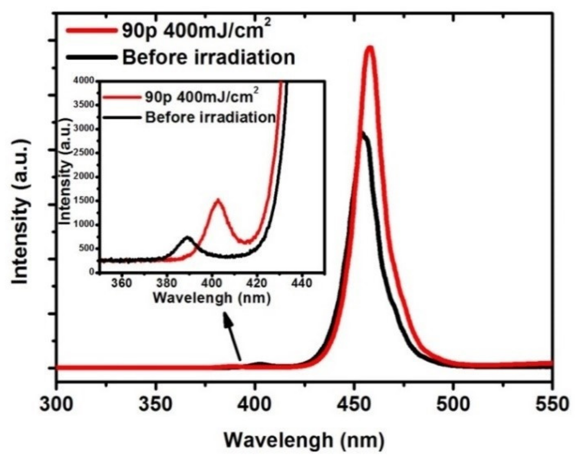
Figure 1 shows the room temperature PL spectra of as-grown and after laser irradiation with specific laser energy density and pulse numbers. The KrF excimer laser irradiated the GaN epitaxial wafers samples with 90 pulses at a repetition rate of 3 Hz. The energy density of the laser was 400 mJ/cm
2. The samples were also irradiated by an energy density of 500 mJ/cm
2 and 600 mJ/cm
2, respectively. We have also investigated the laser-irradiated samples with the same energy density but with different laser pulses. However, damage to the surface of the samples was evident, the PL peak intensity decreased when the sample was irradiated at a laser energy density of 500 mJ/cm
2 or the laser pulse numbers of 100. Therefore, it will be necessary to determine the optimum laser energy density and laser pulse number, in order to effectively enhance
p-type optical and electrical properties of GaN samples with no surface damage.
The inset shows more clearly the intrinsic peak of the PL spectra. It can be seen that the intrinsic peak and the defect peak display a redshift after laser irradiation and this behavior is usually attributed to carrier localization which is common in highly inhomogeneous semiconductor materials and the changing of defect type and content during the laser irradiation. It is also worth noting that the intensity of the PL peaks, including the intrinsic peak and the defect peak, increased about 50% more than the as-grown sample after the laser irradiation. It is well known that the increasing PL intensity is due to the recrystallization of the sample surface, by which the crystalline symmetry was improved significantly. This indicates that a proper energy density of 400 mJ/cm2 and 90 pulses could activate the Mg acceptor and enhance the optical and electrical properties of the GaN material without leading to any deterioration of the optical properties of the sample surface.
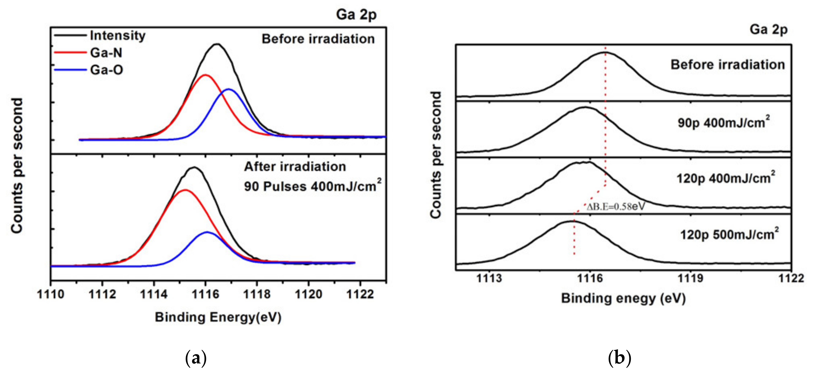
To further investigate the mechanisms of the sample surface during the laser irradiation, XPS was used to analyze the chemical composition of the surface of the GaN epitaxial wafers after laser irradiation at an energy density of 400 mJ/cm
2 and pulse number of 90. In
Figure 2a, the result of the Ga 2
p XPS shows that the Ga-2
p core-level peak shifts toward the lower-energy level side by 0.8 eV, compared with those untreated samples. It means that the shifts in the surface Fermi level toward the valence-band edge attributes to the increased hole concentration of the sample due to the laser irradiation of the
p-GaN surface wafer layer. The results of the XPS also show that there is an oxygen signal before and after laser irradiation. Additionally, we believe that an interfacial oxide layer increases the barrier height for hole injection from metal to
p-GaN films, which results in a detrimental effect for the Ohmic contacts to
p-GaN films. Furthermore, the intensity of the GaO peak energy decreases compared to the untreated sample. As
Table 1 shows, proper laser irradiation improves hole concentration and lowers sheet resistance.
Table 1 also shows that the carrier mobility did not change significantly during the laser irradiation. It is noted that carrier mobility is a critical electrical characteristic that reflects the quality of the sample’s lattice structure. Thus, one can hypothesize that due to the laser irradiation there is no damage to the sample’s lattice structure. To investigate the connection between the shifting Ga-2
p core-level peak position and the corresponding electrical properties,
Figure 2b shows the Ga2
p XPS spectra under different irradiation conditions. We can conclude that the shifting peak position exists under all the irradiated conditions. However, at 120 pulses and 500 mJ/cm
2, compared to the as-grown sample, the shifting extent is nearly 0.58 eV, which is the maximum among the irradiated samples. It is noteworthy that the results of the XPS analysis support the conclusion in
Table 1.
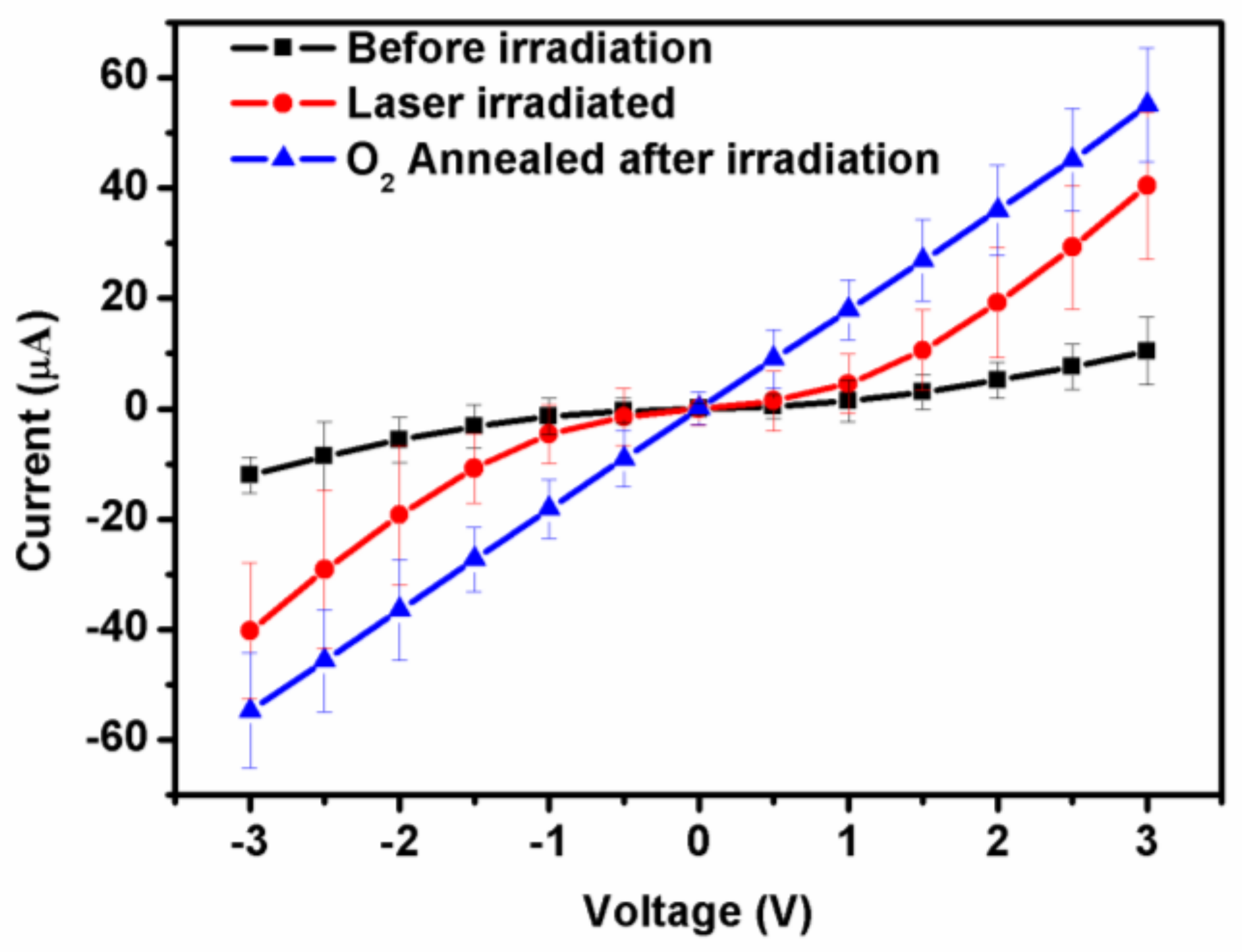
Many previous studies have focused on the individual effect of laser irradiation or annealing treatment, respectively [
24,
25]. In order to compare ohmic contact properties for the laser-irradiated GaN epitaxial wafers and the annealed sample, we conducted I–V characteristic measurement. It is well known that I–V characteristics reflect the contact quality of the GaN epitaxial wafers and the electrode metal, and its quality directly affects the luminescent properties of the GaN-based LED devices.
Figure 3 shows the I–V characteristics for a non-alloyed Ni–Au contact before and after laser irradiation and annealing with O
2. We can see clearly that the I–V characteristics of a sample after irradiation have a rectifying behavior, but with the same forward voltage, the current is larger than the as-grown sample, indicating that an improvement in the sheet resistance and carrier concentration has occurred during the laser irradiation. Furthermore, the O
2-annealed sample after laser irradiation and annealing shows a linear behavior, indicating that the sheet resistance is further reduced and the carrier concentration is further increased during the annealing treatment. We believe that good in ohmic contact was formed after the O
2-annealing treatment.
Table 1 also shows the electrical properties after the annealing treatment.
In order to further investigate the changes of element contents during the laser irradiation, the samples were detected by SIMS, which plays an important role in detecting lighter element contents near the sample surface [
4]. As we all know, using MOCVD growth of GaN epitaxial wafers methods is inevitably uneven sample surface hydrogen content of the element. Since the hydrogen ion has a positive charge, the main coupling unstable compounds such as magnesium would be easily formed and a magnesium-doped
p-type GaN by impurities. We know the Mg–H bond energy of about 1.5 eV, and the photon energy of the KrF excimer laser reaches 5 eV. After the laser irradiation the Mg–H bond acceptor Mg could be activated, so that an improvement in the electrical properties of the sample was achieved. From
Figure 4a it can be seen that, after laser irradiation, the hydrogen near the surface was reduced compared with the sample before irradiation. Hydrogen can be seen in the vicinity of the depth, highlighting the role of laser irradiation to activate the surface acceptor. As we know, the degree of oxidation of the surface of epitaxial wafers can influence its electrical properties. From
Figure 4b, one can see that after laser irradiation, a lower oxygen content was obtained compared to those before the irradiation, indicating that the laser irradiation had caused the release of surface oxide to improve the electrical properties of the sample.
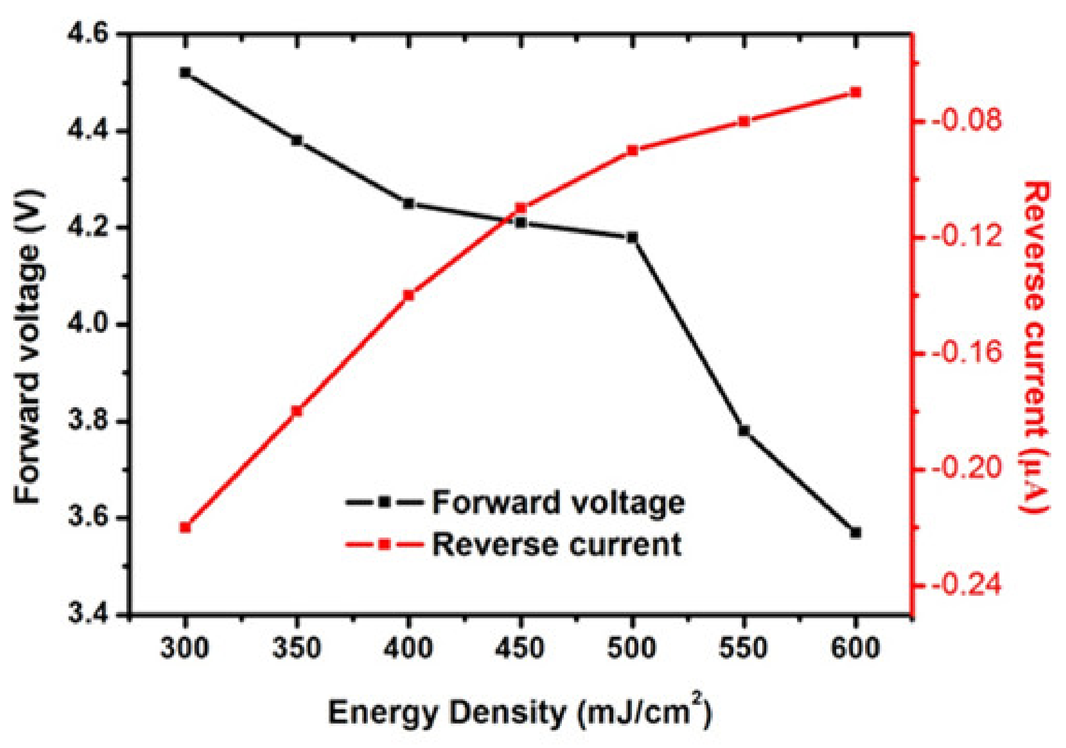
In order to investigate the impact of laser irradiation on the GaN-based LED, I–V characteristics and output power with different energy densities were examined by a conventional technique to test semiconductor light-emitting devices.
Figure 5 shows typical I–V characteristics of the laser-irradiated samples with different laser energy densities. It can be seen that the forward voltages at 20 mA decrease significantly when the energy density becomes larger. Based on a previous report [
4], the decreased forward voltage of the irradiated sample may be attributed to the proper laser-irradiated energy that could activate acceptors without any irreversible damage during the irradiation. The secondary shaft of
Figure 5 shows the reverse I–V characteristics of irradiated samples with different laser energy densities. It is well known that the reverse leakage current is an important criterion of good or bad quality for semiconductor devices. As the energy density increases, the reverse leakage current is measured to be 7.7 × 10
−8 A at the bias of −5 V when the energy density is 600 mJ/cm
2, being smaller than any other irradiated samples. This is considered to be due to the presence of more dislocations in InGaN/GaN MQWs and improvement in the quality of GaN-based LED devices.
To compare the luminescent properties of O
2-annealed and only laser-irradiated samples, L–I characteristics were measured at an injection current of 20 mA.
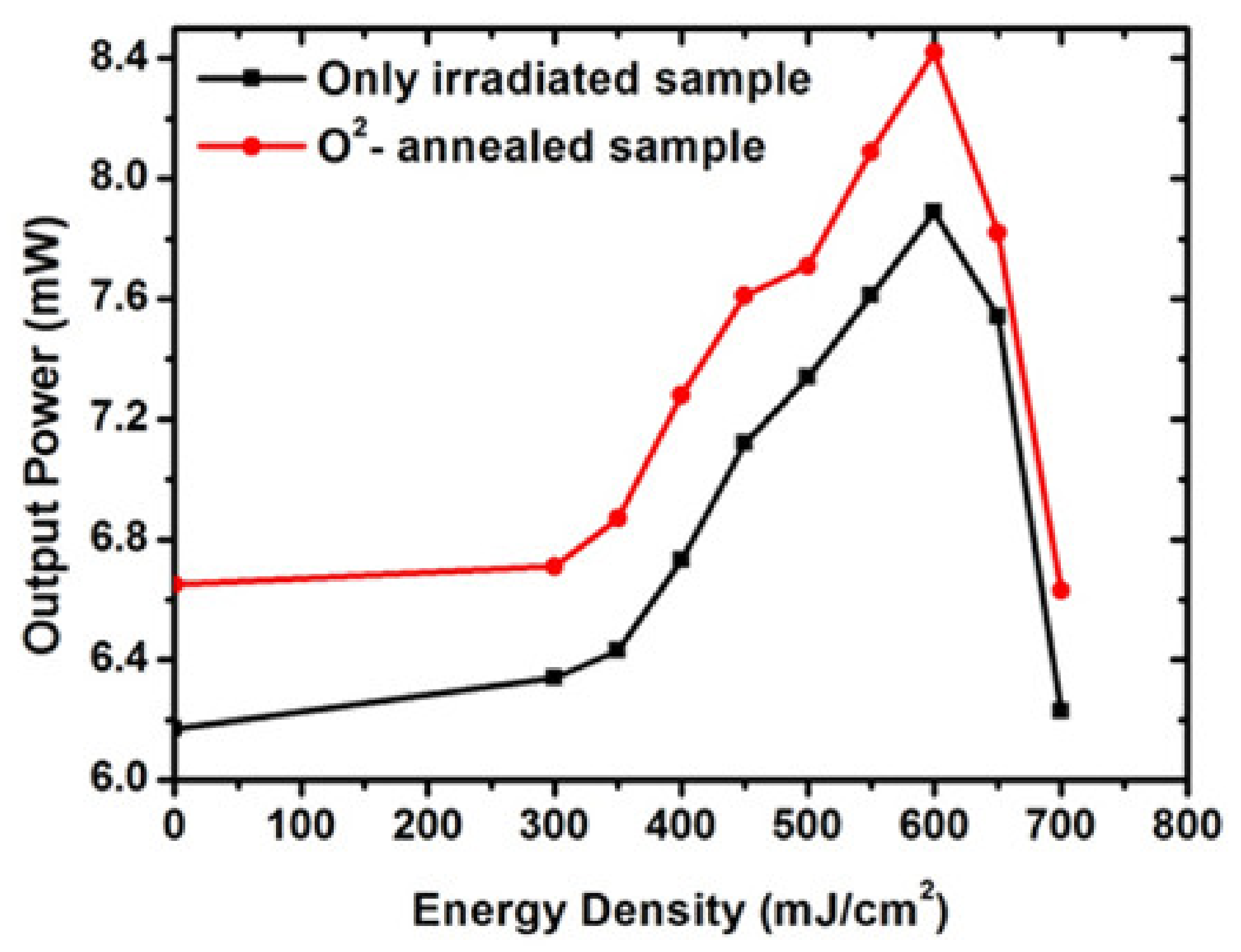
Figure 6 shows that the light output power of O
2-annealed and only laser-irradiated LEDs at different laser energy densities during the irradiation. The O
2-annealed samples show better performance at light output power at any laser energy density compared to the laser-irradiated samples. It is worth mentioning that under appropriate laser conditions with pulse numbers of 90 at an energy density of 400 mJ/cm
2 and O
2-activated annealing, the light output of the laser-irradiated GaN-based LED sample is about 1.44 times that of a conventional LED at 20 mA, and it is found that wall-plug efficiency is 10% higher at 20 mA, the reverse leakage current is 80% lower at 5 V. These results imply that annealing in O
2 ambient is a necessary step to enhance the luminescent properties of GaN-based LED.


