Article

28 GHz Single-Chip Transmit RF Front-End MMIC for Multichannel 5G Wireless Communications

1
Tomsk State University of Control Systems and Radioelectronics, 634050 Tomsk, Russia
2
Institute of Atmospheric Optics V.E. Zuev SB RAS, 634055 Tomsk, Russia
3
Research and Production company Micran, 634045 Tomsk, Russia
*
Author to whom correspondence should be addressed.
Symmetry 2020, 12(7), 1167; https://doi.org/10.3390/sym12071167
Submission received: 15 June 2020 / Revised: 6 July 2020 / Accepted: 8 July 2020 / Published: 14 July 2020
(This article belongs to the Special Issue Information Technologies and Electronics)

Abstract

:
Millimeter-wave wireless networks of the new fifth generation (5G) have become a primary focus in the development of the information and telecommunication industries. It is expected that 5G wireless networks will increase the data rates and reduce network latencies by an order of magnitude, which will create new telecommunication services for all sectors of the economy. New electronic components such as 28 GHz (27.5 to 28.35 GHz) single-chip transmit radio frequency (RF) front-end monolithic microwave integrated circuits (MMICs) will be required for the performance and power consumption of millimeter-wave (mm-wave) 5G communication systems. This component includes a 6-bit digital phase shifter, a driver amplifier and a power amplifier. The output power P3dB and power-added efficiency (PAE) are 29 dBm and 19.2% at 28 GHz. The phase shifter root-mean-square (RMS) phase and gain errors are 3° and 0.6 dB at 28 GHz. The chip dimensions are 4.35 × 4.40 mm.

1. Introduction

The population of our planet is gradually increasing and has already exceeded 7 billion people. The information needs of the population are growing; at the same time, new technologies such as the Internet of Things (IoT), intelligent transport systems (such as Vehicular Ad hoc Network (VANETs)) and virtual and augmented reality are actively developing [1]. The growth of data traffic and device connections will require data rates to increase by more than an order of magnitude [2]. Responding to these requests, the International Telecommunication Union (ITU) decided to develop a new generation of 5G wireless communications with high transmission speeds (>10 Gbit/s) and ultralow response times (<1 ms). However, an increase in the transmission date rate is mainly possible due to the expansion of the band that the frequencies use. The requirements for 5G networks can only be implemented in the millimeter-wave frequency range [3].
The advantages of millimeter waves (mm-waves) when used for radio communications have been well known for many years [4]. The advantageous features of millimeter-wave radio waves are responsible for their widespread use in radar systems, remote sensing, navigation and communications. Interest in millimeter waves has increased due to the need to expand the radio frequency spectrum for commercial applications. Compared with previous generations, mm-wave 5G wireless communication systems have higher data rates and data transfer density, millisecond latency and enhanced spectral energy. The International Telecommunication Union (ITU) has specified a number of the mm-wave frequency bands for 5G [5] wireless networks, but the 27.5–28.35 GHz band was proposed for wide usage in many countries and was licensed by the Federal Communications Commission (FCC) [6].
Power consumption is one of the most significant technical barriers for practical mm-wave 5G wireless communications because multiple devices connected at the same time increase the power consumption of the base stations and data centers. Photonic technologies can be utilized in order to solve this problem. In data centers, chip-to-chip optical or electro-optical interconnects enable an increase in the bandwidth and capacity of those systems as well as a reduction in power consumption [7,8].
In a conventional 4G communication system, one or more passive antennas are used. Wireless 5G networks are based on active massive-element antenna systems that improve the capacity, efficiency and coverage of RF streams [9] (Figure 1).
To improve the bandwidth and data rate, the multiple-input multiple-output (MIMO) transceivers based on phased beamforming arrays are used [10,11,12,13]. Usually, active antenna systems consist of massive antenna arrays with integrated MIMO transceiver RF front-ends.
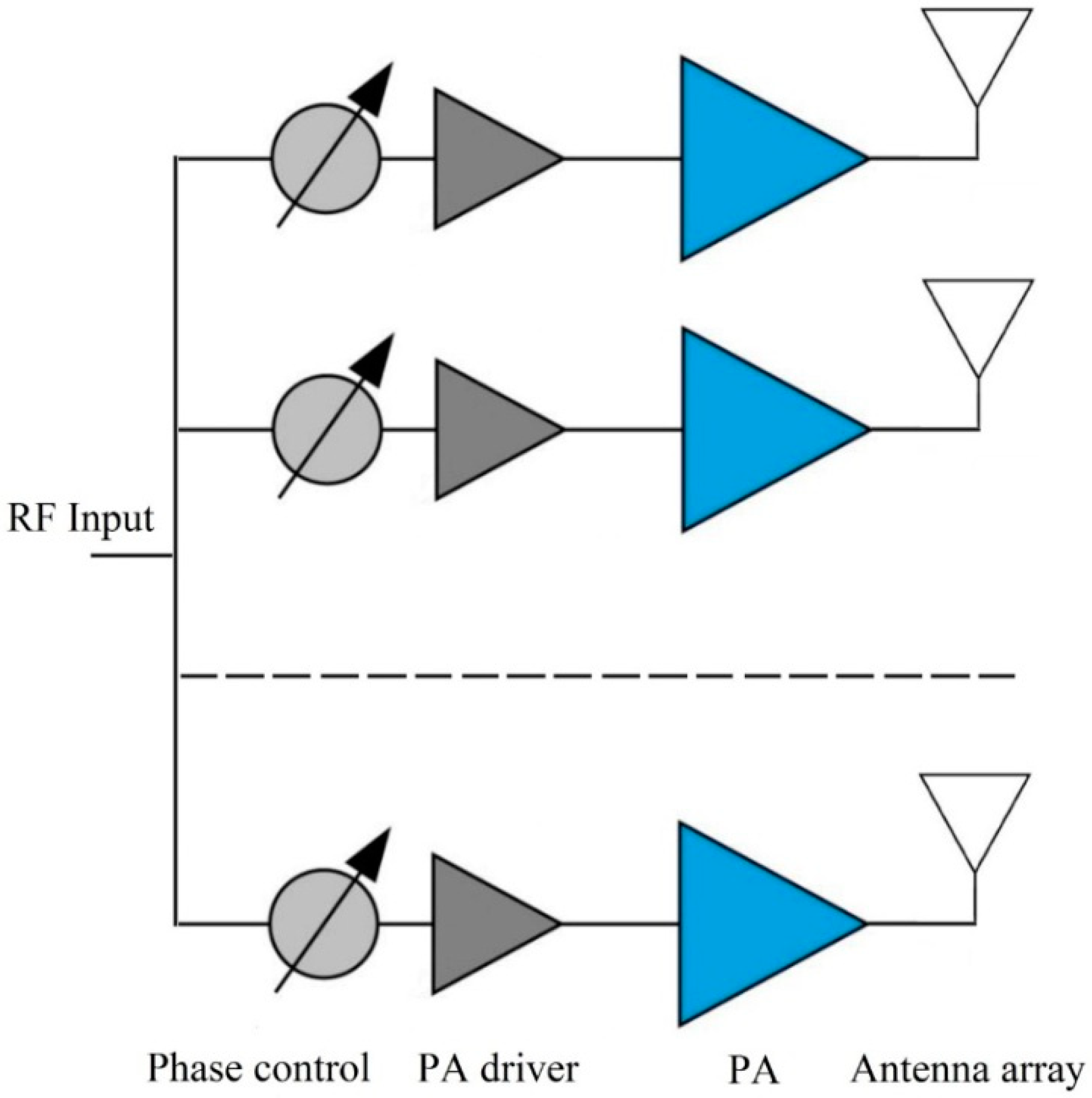
Figure 2 shows the design of a multichannel transmit RF front-end (RFFE) module for 5G MIMO transceivers. There is a symmetrical antenna array where each channel consists of a phase shifter, a driver amplifier and a power amplifier. The input splitter divides the RF signal into a number of channels. The symmetry of the RFFE module architecture allows for a balance between input and output losses and power consumption.
The performance and power consumption of millimeter-wave 5G communication systems are mainly dependent on the electrical parameters of using RF electronic components based on semiconductor monolithic integrated circuits, which are the key elements for mm-wave RF transmit/receive modules. The development of such elements is a difficult challenge.
A previous study presented the results of the development of a 28 GHz phase adjustable power amplifier monolithic microwave integrated circuit (MMIC) for 5G front-ends [14]. It consisted of a 4-bit digitally controlled phase shifter and power amplifier. The MMIC was designed by Plextek RFI and fabricated by Win Semiconductors using a 0.15 µm GaAs pHEMT process. The main disadvantage of this MMIC is a low phase shift resolution of 22.5°, which results in reduced beamforming opportunities and low antenna gain.
In this study, the design approach for a 28 GHz single-chip transmit RFFE MMIC with high phase shift resolution (5.625°) for multichannel 5G wireless communications is presented, along with its electrical performance. The integrated circuit (IC) consists of a 6-bit digital phase shifter, a driver amplifier and a power amplifier and was designed using a 0.25 µm GaAs pHEMT process of JSC Micran (Tomsk, Russian Federation) for low-cost volume production.

2. Single-Chip RF Front-End MMIC

2.1. Design Approach

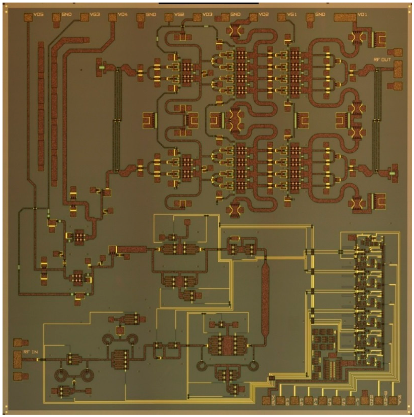
Figure 3 shows a photo of a fabricated one-channel single-chip transmit RF front-end MMIC. The chip dimensions are 4.35 mm × 4.40 mm. The single-chip IC consists of a 6-bit phase shifter with a transistor-transistor logic (TTL) driver, a driver amplifier and a power amplifier (PA) and was designed using a 0.25 µm GaAs pHEMT process for low-cost volume production.
The phase shift level of a single-chip transmit RFFE MMIC is controlled by an integrated TTL driver. The 6-bit digital driver can precisely adjust a phase from 0 to 360° with a step of 5.625°. Table A1 in Appendix A shows the phase shifter state table. There are two control levels (0 and 1) for all bits. Low (0) and high (1) TTL control levels are 0 and +5 V. Applying different control levels for all 6 bits of the digital phase shifter may change the phase shift across the full 360° range.
The high- and low-pass (HP-LP) RF filters were used to design the 6-bit digital phase shifter [15]. The applied TTL control voltages across all bits allowed the switching of states between HP-LP filters to form the required output phase shift level. This solution exhibits good return losses, phase shift performance in RMS phase and gain errors.
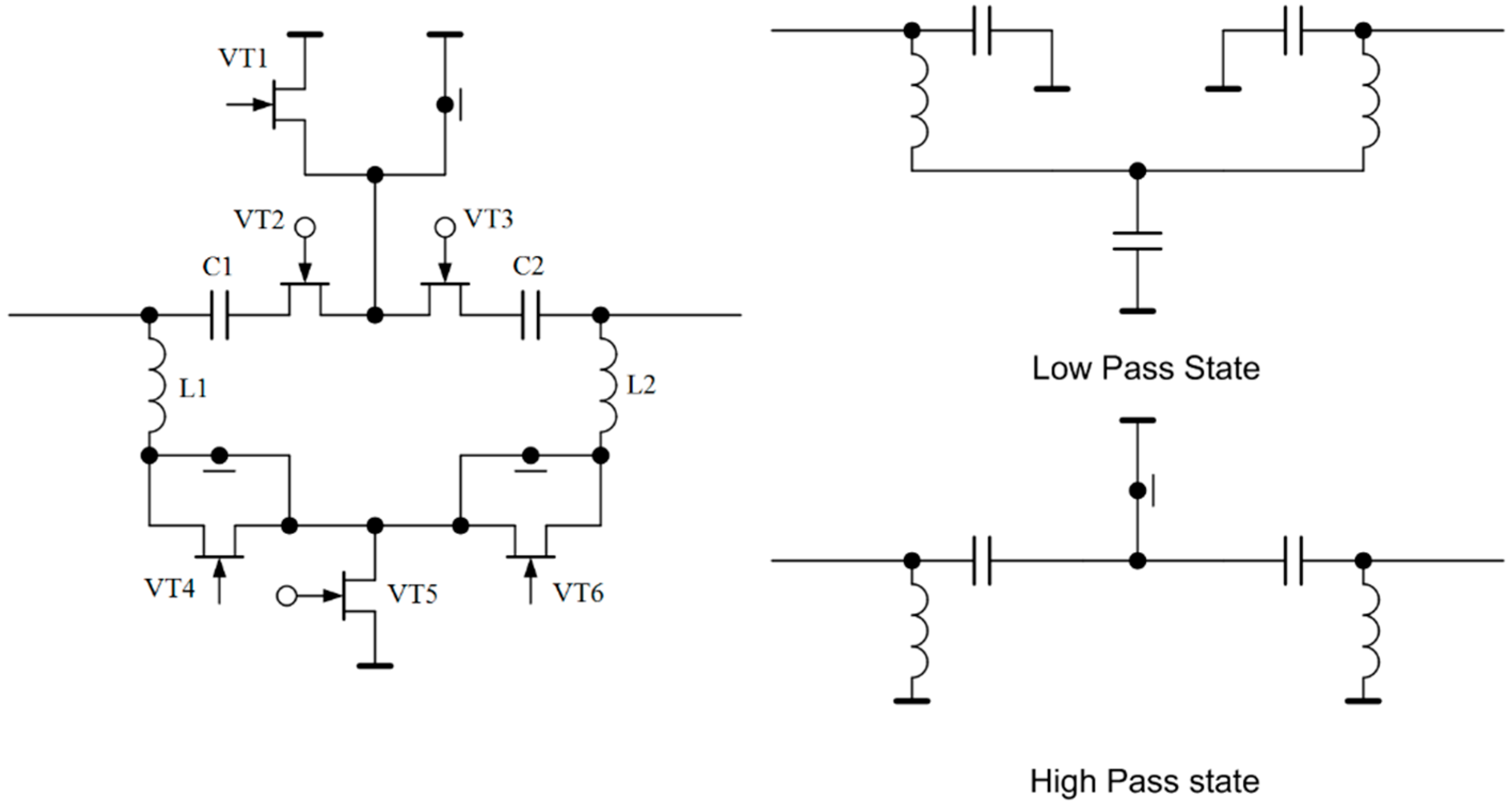
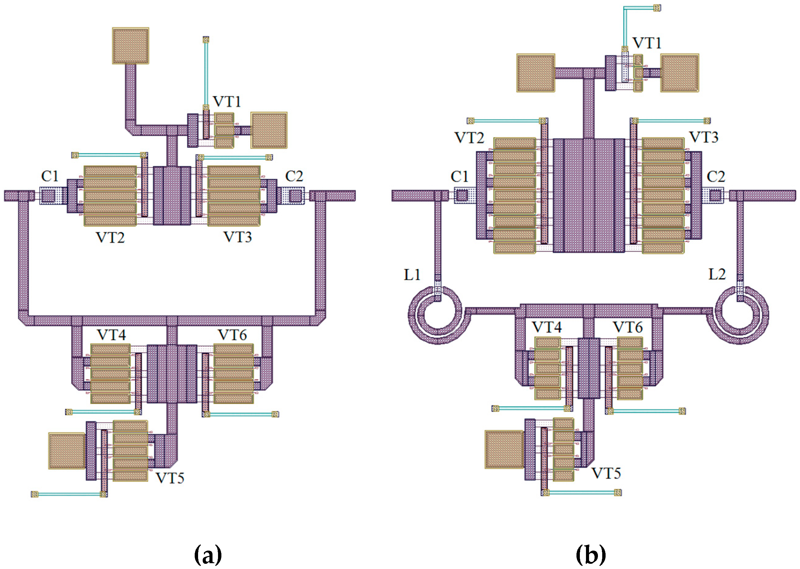
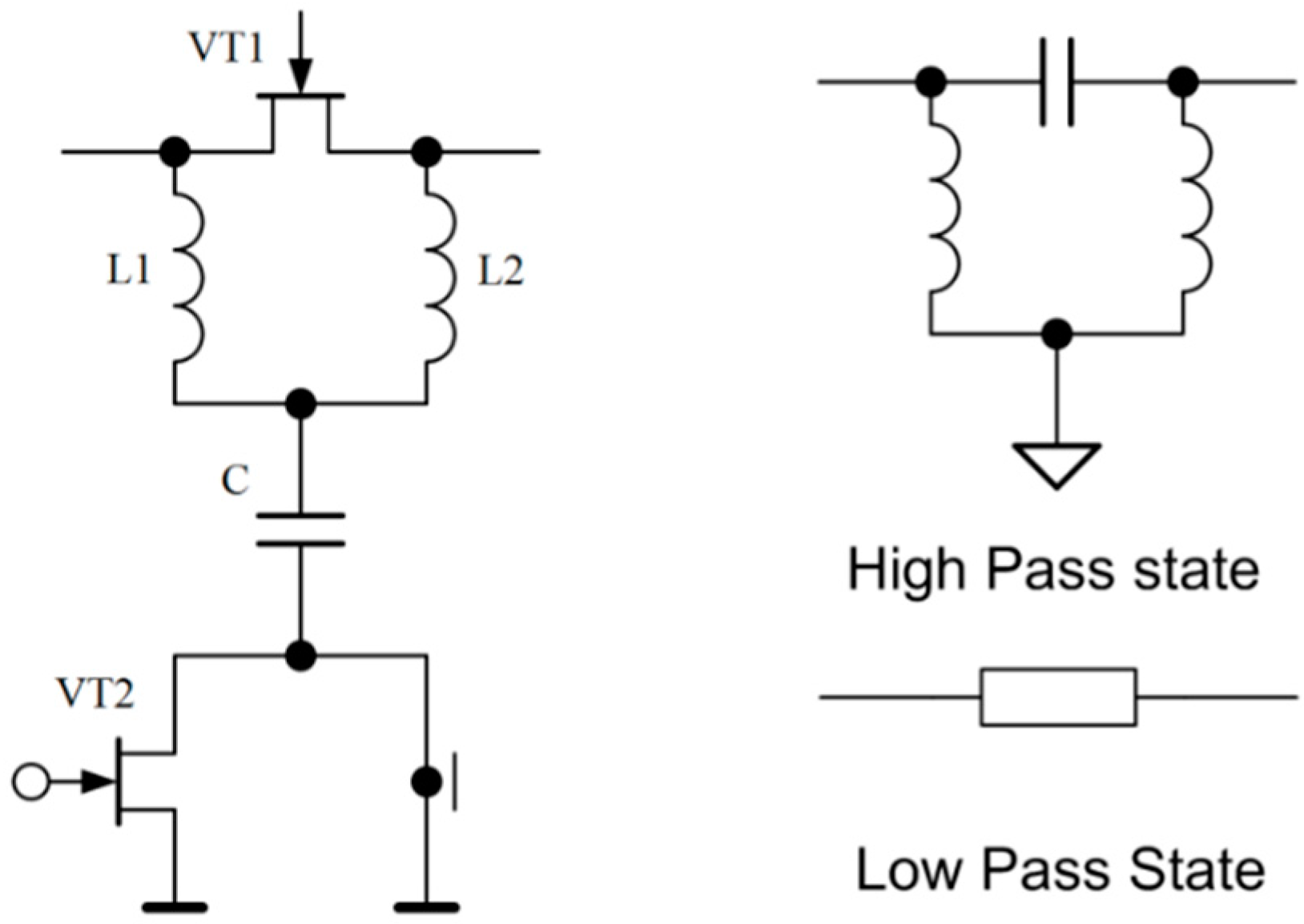
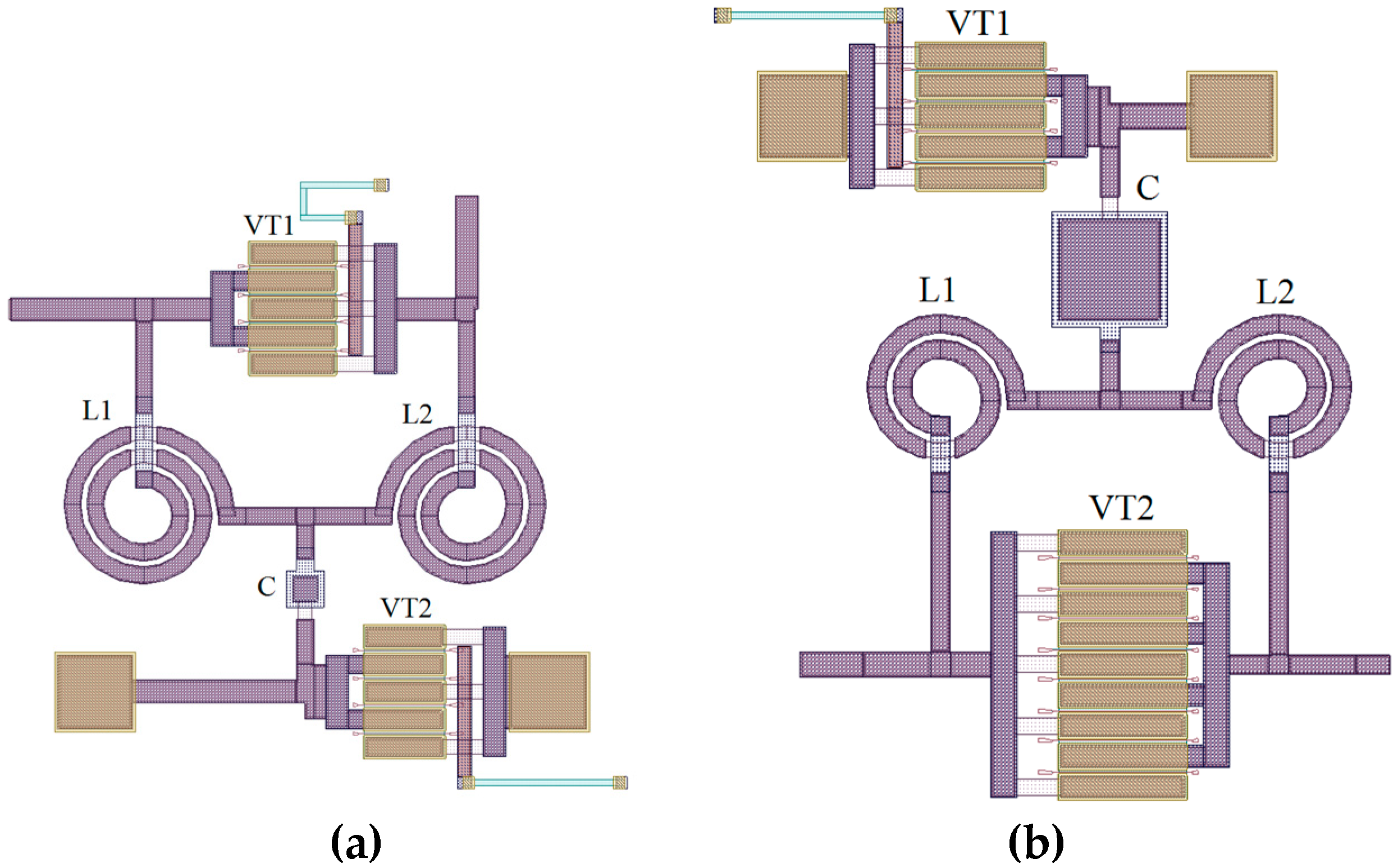
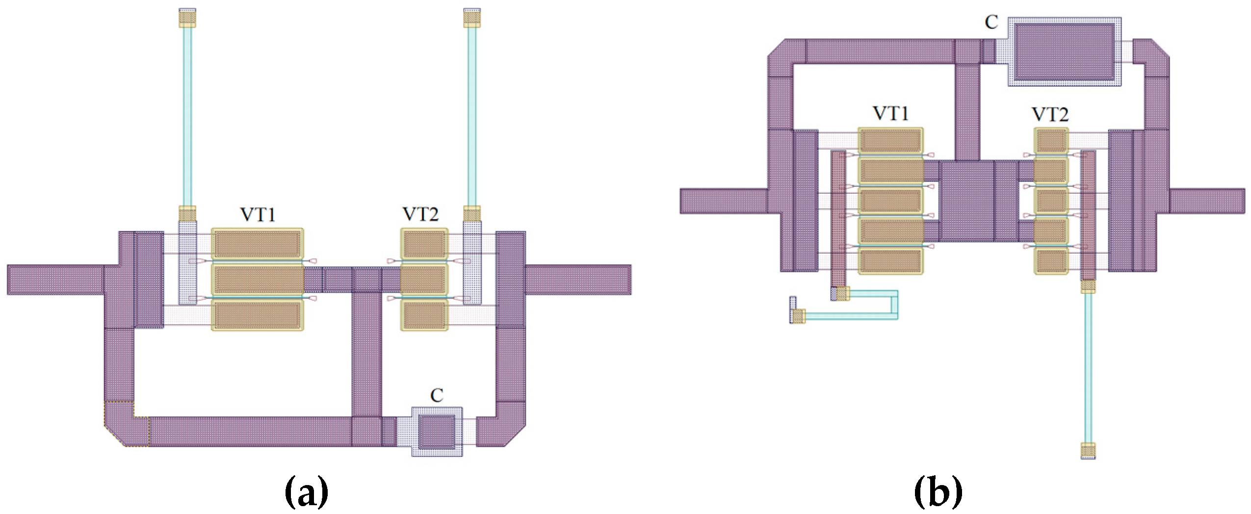
The electrical schemes and layout plots of 180, 90, 45, 22.5, 11.25 and 5.625° bits are presented in Figure 4, Figure 5, Figure 6, Figure 7, Figure 8 and Figure 9. For 180 and 90° bits, a circuit was selected with switchable filters using an inactive arm in the filter. The classical solution of using switchable filters does not provide a sufficient level of decoupling of the active and inactive arms, which leads to an increase in the initial bit losses. The 45 and 22.5° bits were designed according to the scheme with switched elements in the filter. This is the only possible solution for the 27.5–28.35 GHz band. For 11.5 and 5.625° bits, a circuit was designed with a serial connection of filters due to a very small inductance. In this circuit, the inductance is shunted because the required phase shift requires a large length of the microstrip.
The choice in the order of the phase shifter bits was carried out strictly on the principle of minimal influence of the reflection coefficient between the bits. To do this, the sections with the lowest similarity of the reflection coefficient are placed between the sections with the highest similarity of the reflection coefficient. The most stable bits are 180 and 90°, and the least stable bits are 11.25 and 5.625°. Therefore, the optimal bit ordering is selected as follows: 22.5 to 11.25 to 90 to 5.625 to 180 to 45°. This ordering allows the RMS phase shift error to be reduced.
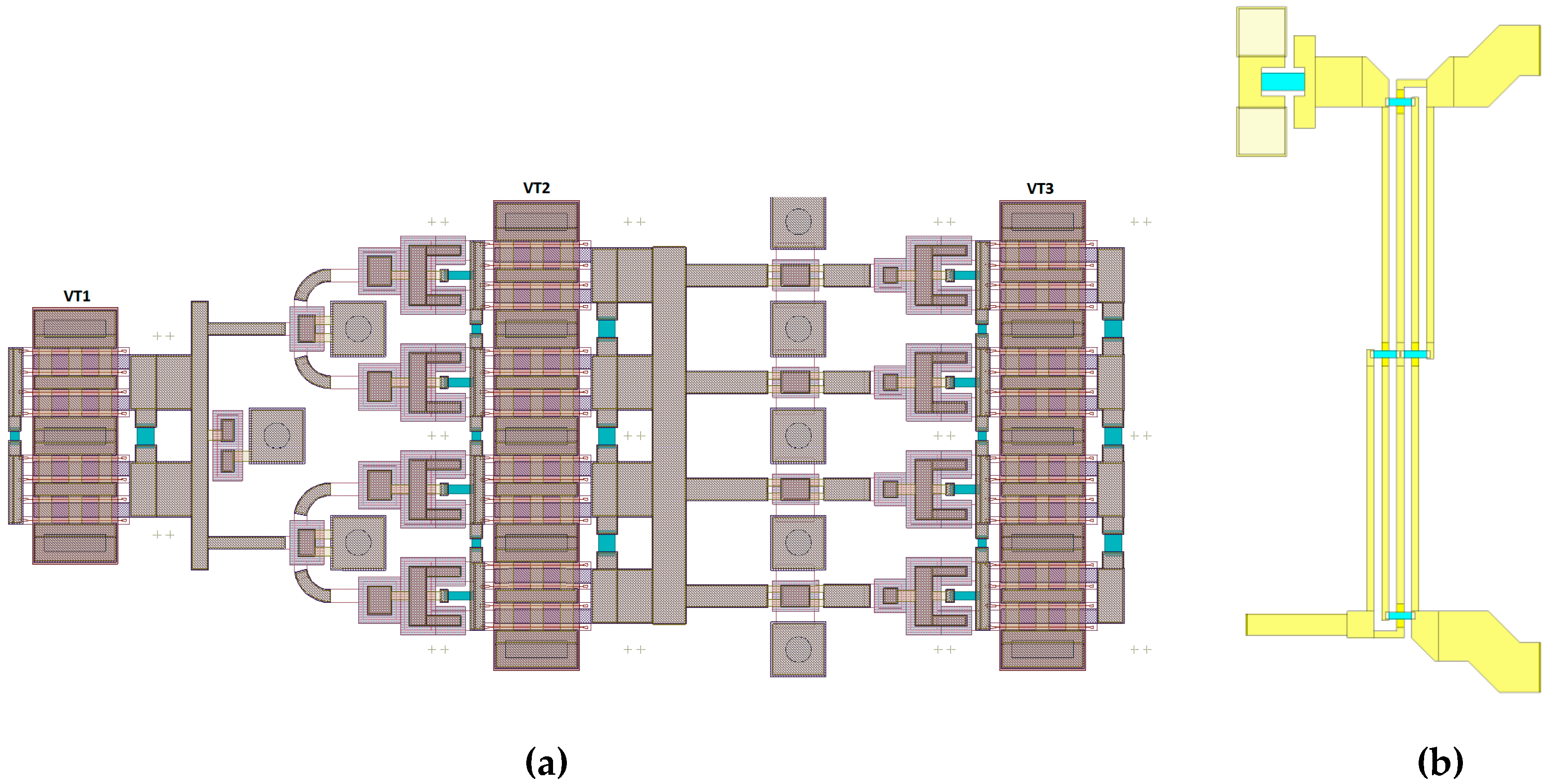
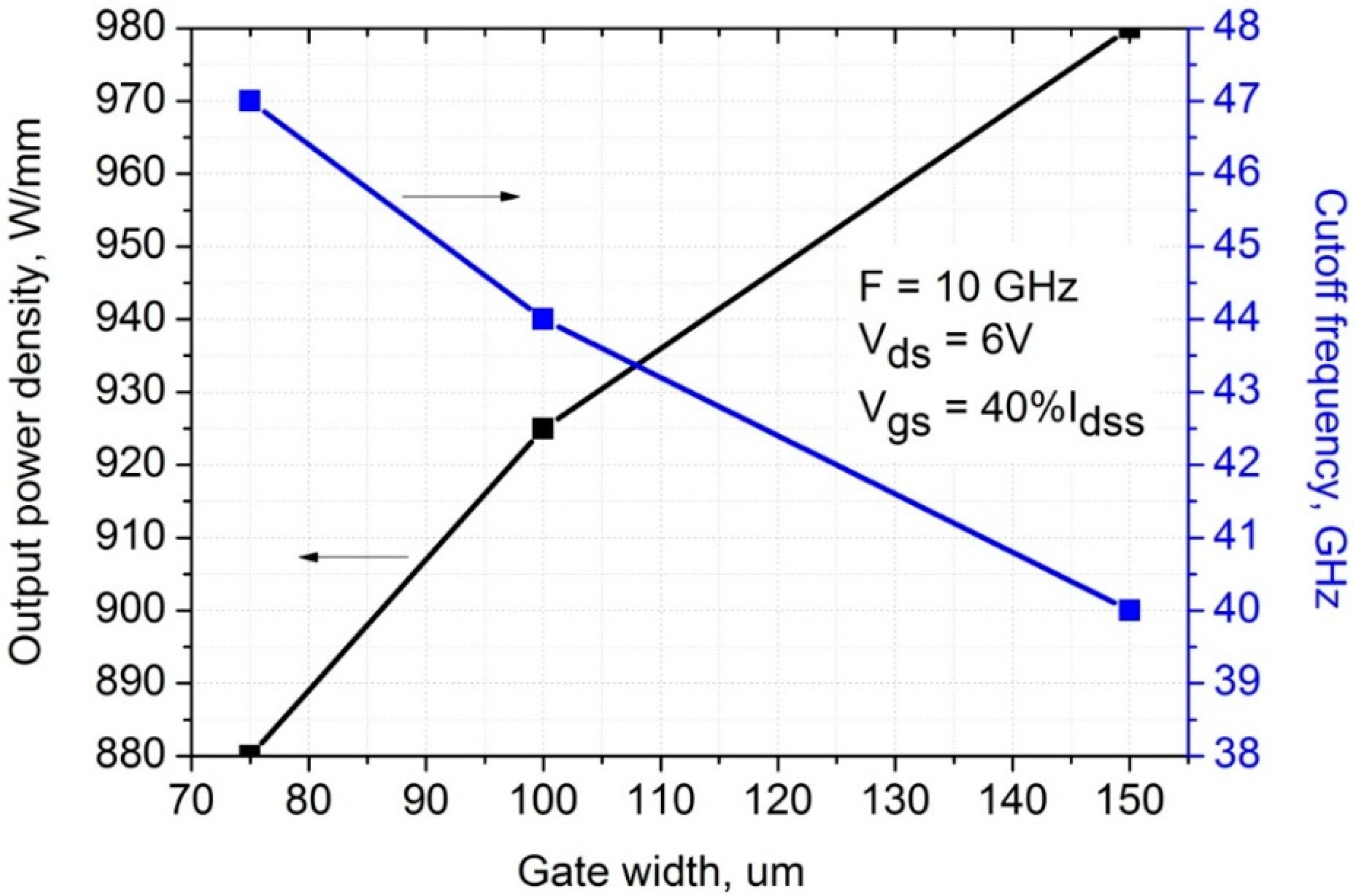
The power amplifier (PA) of a single-chip transmit front-end MMIC consists of three power stages and matching networks (Figure 10a). The base active element of the PA is a GaAs pHEMT with a 0.25 µm length gate. To achieve a balance between output power capability and cutoff frequency, the transistor gate width is 100 µm (Figure 11). The increase in gate width can improve the output power of the transistor, but higher parasitic capacitance will reduce the cutoff frequency. The peripheries of the transistors are 1600 µm (16 × 100 µm) for the first stage (Q1), 3200 µm (32 × 100 µm) for the second stage (Q2) and 3200 µm (32 × 100 µm) for the third stage (Q3). The supply voltage for all power stages is Vd = 6 V.
The matching networks of the power amplifier consist of thin-film NiCr-based resistors, metal-insulator-metal (MIM) capacitors based on silicon nitride, Au-based transmission lines and Lange quadrature couplers (LQCs). The proposed LQCs (Figure 10b) are used in input and output matching networks to improve the bandwidth and achieve a compact PA size. The symmetrical design of the PA layout and electromagnetic simulation were completed at the AWR Microwave Office [16].

2.2. Electrical Performance

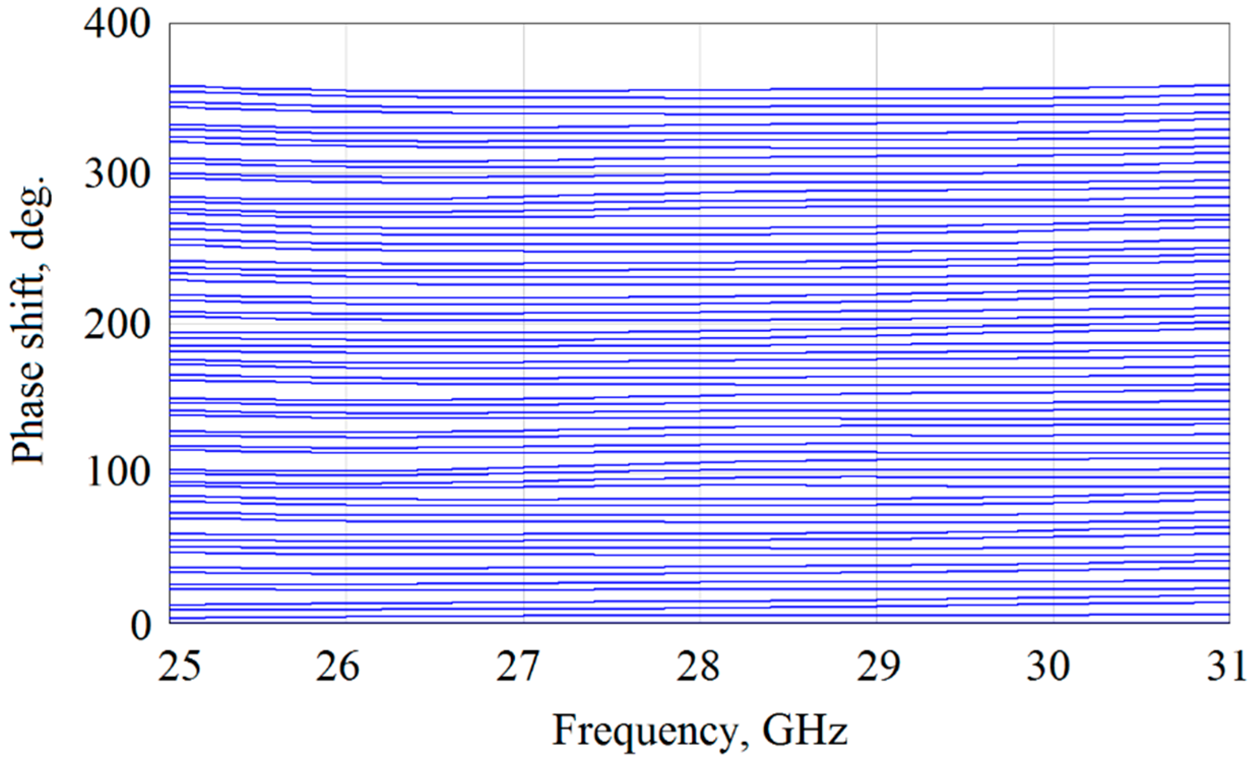
Figure 12 shows the dependences of the simulated phase shift performance on the frequency for 64 states of a one-chip RF front-end MMIC.
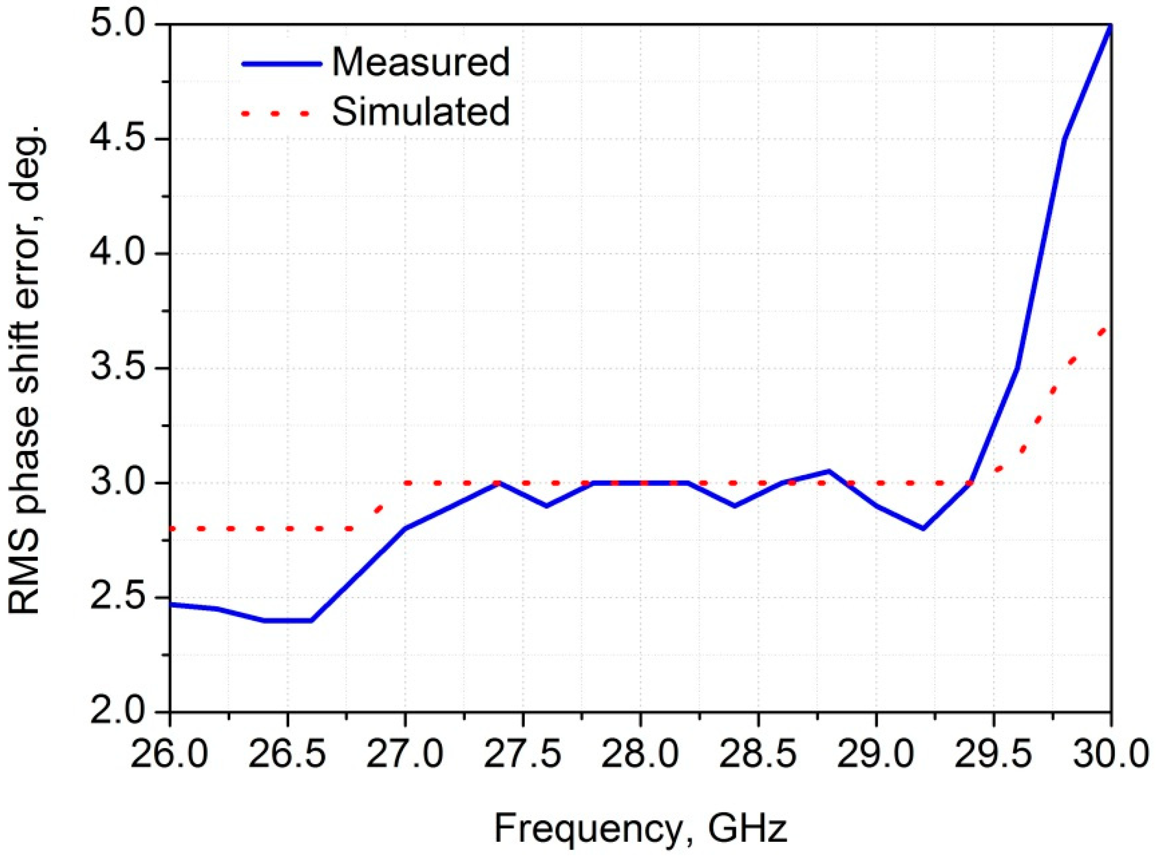
Figure 13 shows the dependence of the RMS phase shift error (PSE) of the single-chip RF front-end MMIC on frequency in the range of 26 to 30 GHz. The measured RMS PSE was calculated according to Equation (1):
σ φ = ( ε φ 1 ε φ ) 2 + ( ε φ 2 ε φ ) 2 + + ( ε φ ( N 1 ) ε φ ) 2 N = i = 1 N 1 ( ε φ i ε φ ) 2 N
where N is the number of phase states number, εφ is the measured phase shift in degrees and <εφ> is the average phase shift for states of the 6-bit phase shifter.
According to the results presented in Figure 13, RMS phase shift error is about 3° across the entire 27.5–28.35 GHz range.
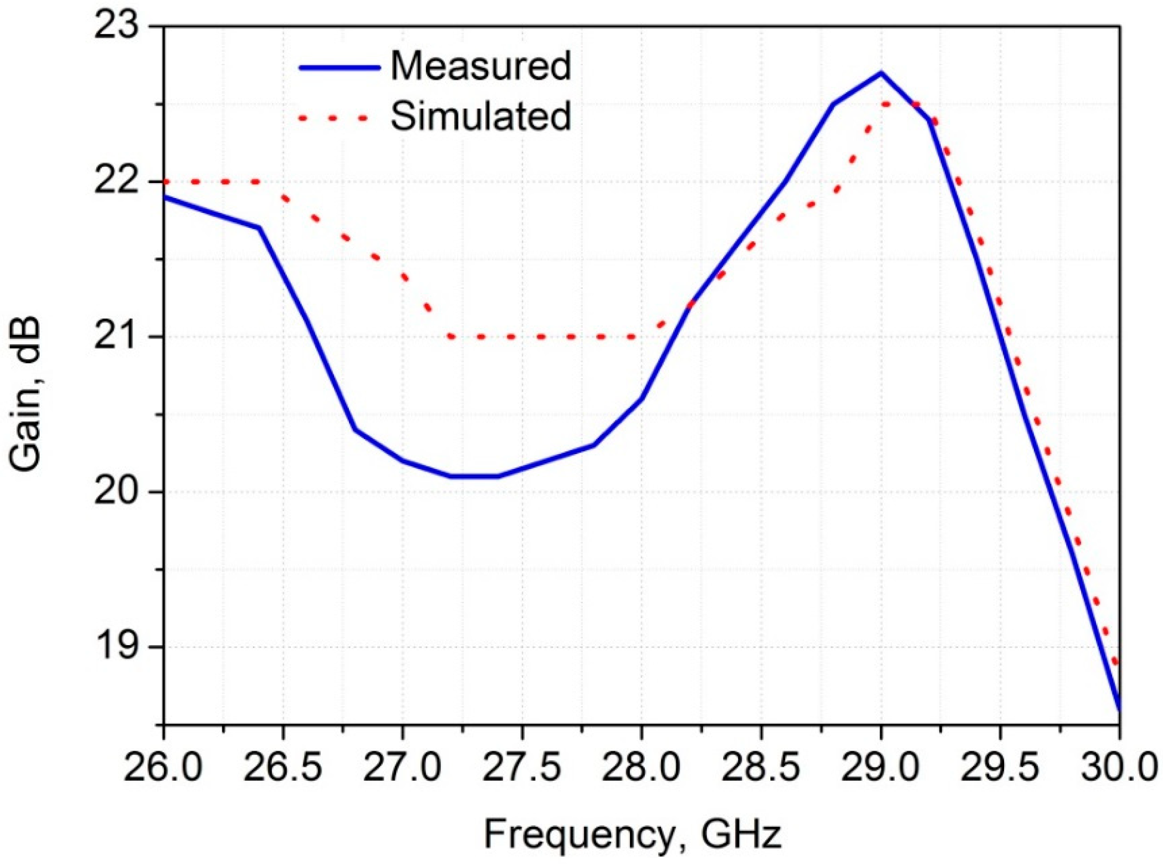
Figure 14 shows the dependence of small signal gain in all phase states of the single-chip RF front-end MMIC on frequency in the 26 to 30 GHz frequency range. There is a nominal small signal gain of over 20 dB in the frequency range of 27.5 to 28.35 GHz. The maximum gain of 22.7 dB is achieved at 29 GHz.
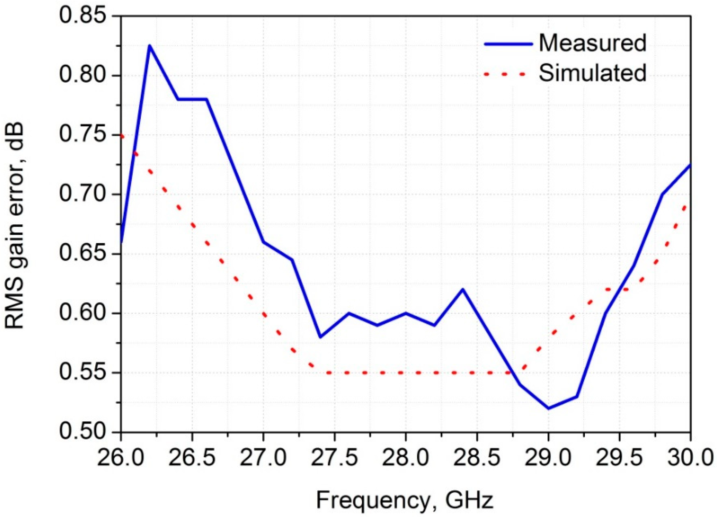
Figure 15 shows the dependence of RMS gain error (GE) of the single-chip RF front-end MMIC on frequency in the 26 to 30 GHz frequency range. The measured RMS (GE) was calculated according to Equation (2):
σ | S 21 | = i = 0 N 1 ( | S 21 | i | S 21 | ) 2 N
where N is the number of phase states, |S21| is the measured gain in dB and <|S21|> is the average gain for states of the 6-bit phase shifter.
According to the results presented in Figure 15, RMS GE is 0.6 dB for the entire 27.5–28.35 GHz range.
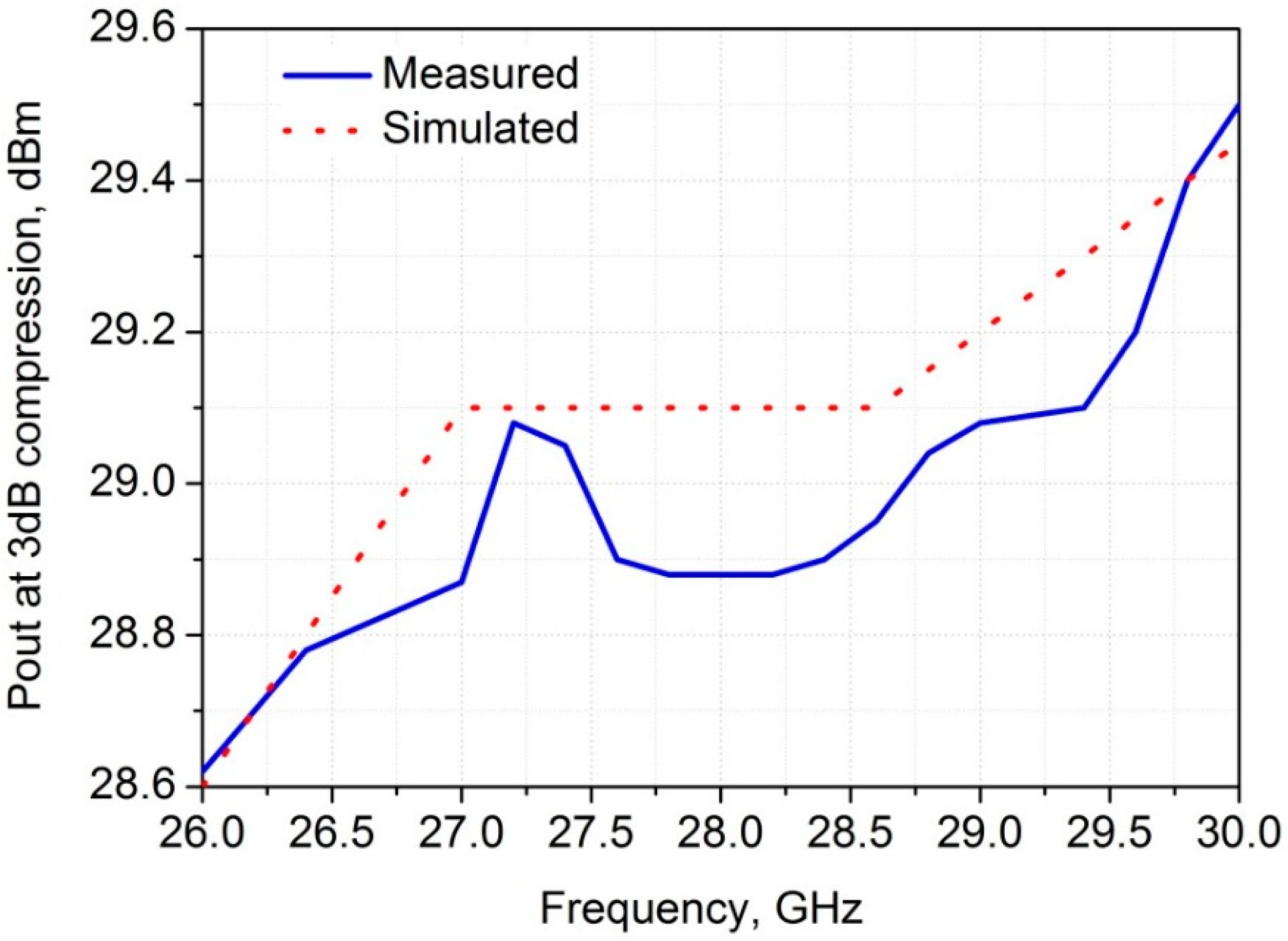
Figure 16 shows the dependence of the output power capability at 3 dB gain compression (P3dB) for the 0° phase state of the single-chip RF front-end MMIC on frequency. The output power P-3dB is 29 dBm across the full 27.5 to 28.35 GHz band. The maximum P3dB of about 29.5 dBm is achieved at 30 GHz.
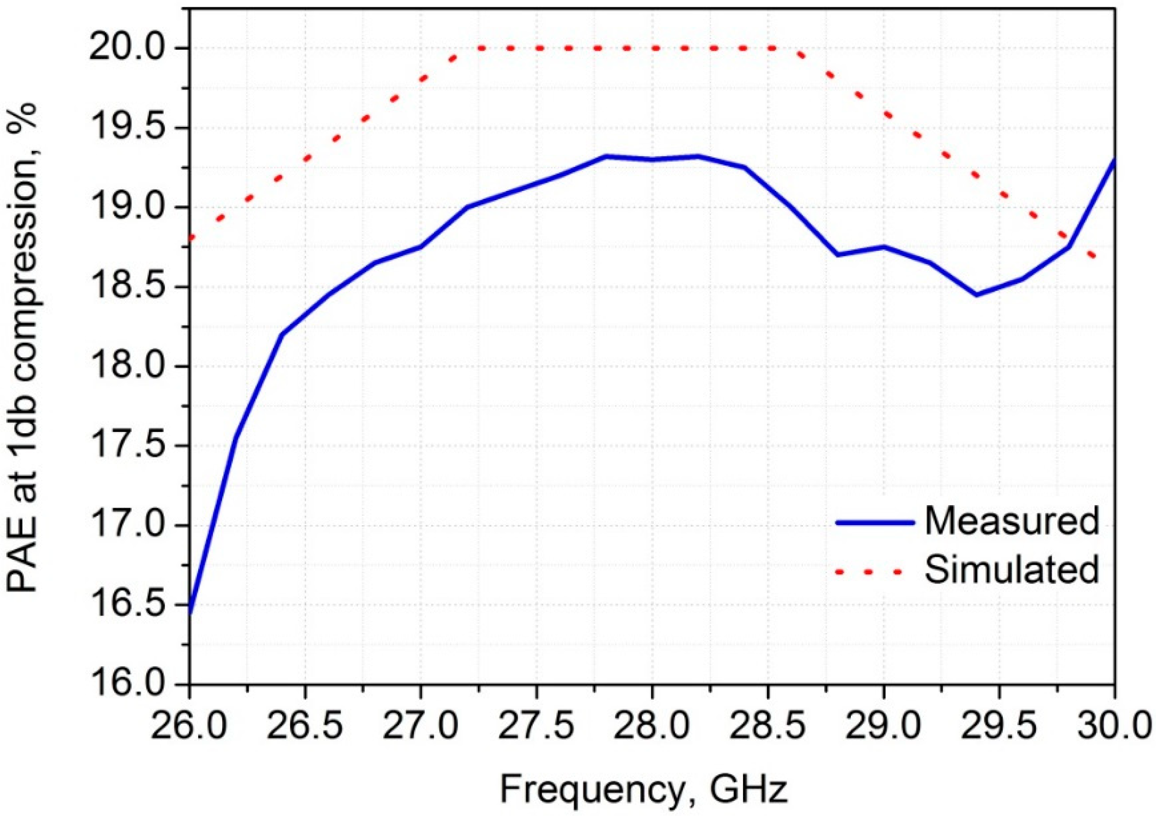
Figure 17 shows the power-added efficiency (PAE) at 1 dB gain compression for the 0° phase state of the single-chip RF front-end MMIC frequency. A maximum PAE of 19.3% is achieved in the 27.5 to 28.35 GHz frequency range. Further optimization of the input and output matching networks in power amplifier stages can improve the PAE and the output power capability.
Table 1 shows the electrical performance of the developed single-chip transmit RFFE MMIC in comparison with state-of-the-art single-chip transmit RFFE MMICs [14]. The fabricated MMIC has a comparable performance and a higher phase shift resolution. The improved output power and PAE of the RF front-end presented in [14] can be attributed to the use of the 0.15 µm GaAs pHEMT process of Win Semiconductors, with lower gate length resulting in better high-frequency performance.

3. Conclusions

Millimeter-wave wireless networks have attracted the most interest as 5G communication systems of the new generation (5G). The 27.5 to 28.35 GHz band was licensed for 5G wireless networks by the FCC. The performance and power consumption of millimeter-wave 5G communication systems mainly depend on the electrical parameters of the electronic RF components used inside RF transmit/receive modules.
The design approach for a 28 GHz single-chip transmit RF front-end MMIC is presented in this paper, along with its electrical performance. The IC includes a 6-bit digital phase shifter, a driver amplifier and a power amplifier. It was designed using a 0.25 µm GaAs pHEMT process for low-cost volume production. The output power P3dB and PAE are 29 dBm and 19.2% at 28 GHz. The phase shifter RMS phase and gain errors are 3° and 0.6 dB at 28 GHz. The fabricated single-chip RF front-end MMIC can be used in multichannel transmit 5G front-end modules based on phased antenna arrays.

Author Contributions

Conceptualization, V.A.; methodology, V.A.; software, M.S.; validation, M.S.; formal analysis, A.V.; investigation, A.K. and V.K.; resources, M.S.; data curation, E.E.; writing—original draft preparation, E.E.; writing—review and editing, E.E.; visualization, A.K. and V.K.; supervision, E.E.; project administration, E.E.; funding acquisition, V.A. and E.E. All authors have read and agreed to the published version of the manuscript.

Funding

The work was carried out with financial support from the Ministry of Science and Higher Education of the Russian Federation (Project name: Theoretical and experimental studies of ultra-wideband optoelectronic devices of fiber-optic information systems and radiophotonics based on photonic integrated circuits own development, Agreement No. 075-03-2020-237/1 from 05.03.2020, project number: FEWM-2020-0040) and Project No. AAAA-A19-119110690036-9. Experimental results were obtained by the team of the Integrated Optics and Radiophotonics Laboratory of the Tomsk State University of Control Systems and Radioelectronics using equipment of the “Impulse” center of collective usage (registration number 200568).

Conflicts of Interest

The authors declare no conflict of interest.

Appendix A

Table A1. Phase shifter state table («0» is low control level and «1» is high control level).
Bit1Bit2Bit3Bit4Bit5Bit6Relative Phase Shift, deg.
0000000.000
1000005.625
01000011.250
11000016.875
00100022.500
10100028.125
01100033.750
11100039.375
00010045.000
10010050.625
01010056.250
11010061.875
00110067.500
10110073.125
01110078.750
11110084.375
00001090.000
10001095.625
010010101.250
110010106.875
001010112.500
101010118.125
011010123.750
111010129.375
000110135.000
100110140.625
010110146.250
110110151.875
001110157.500
101110163.125
011110168.750
111110174.375
000001180.000
100001185.625
010001191.250
110001196.875
001001202.500
101001208.125
011001213.750
111001219.375
000101225.000
100101230.625
010101236.250
110101241.875
001101247.500
101101253.125
011101258.750
111101264.375
000011270.000
100011275.625
010011281.250
110011286.875
001011292.500
101011298.125
011011303.750
111011309.375
000111315.000
100111320.625
010111326.250
110111331.875
001111337.500
101111343.125
011111348.750
111111354.375

References

  1. Osseiran, A. 5G Mobile and Wireless Communications Technology; Cambridge University Press: Cambridge, UK, 2016. [Google Scholar]
  2. Agiwal, L.; Roy, A.; Saxena, N. Next generation 5G wireless networks: A comprehensive survey. IEEE Commun. Surv. Tutor. 2016, 18, 1617–1655. [Google Scholar] [CrossRef]
  3. Marcus, M. 5G and “IMT for 2020 and beyond”. IEEE Wirel. Commun. Mag. 2015, 22, 2–3. [Google Scholar] [CrossRef]
  4. Albreem, M. 5G wireless communication systems: Vision and challenges. In Proceedings of the 2015 International Conference on Computer, Communications, and Control Technology (I4CT) 2015, Kuching, Malaysia, 21–23 April 2015; pp. 493–497. [Google Scholar]
  5. International Telecommunications Union. 2019. Available online: http://www.itu.int/en/ITU-R/study-groups/rsg5/rwp5d/imt-2020/Pages/default.aspx (accessed on 1 July 2020).
  6. Federal Communications Commission 2020: Upper Microwave Flexible Use Service Millimeter Frequency Bands. Available online: https://www.fcc.gov/wireless/bureau-divisions/broadband-division/upper-microwave-flexible-use-service-umfus (accessed on 1 July 2020).
  7. Testa, F.; Pavesi, L. Optical Switching in Next Generation Data Centers; Springer International Publishing: Cham, Switzerland, 2018. [Google Scholar]
  8. Liu, X. Emerging optical access network technologies for 5G wireless. IEEE/OSA J. Opt. Commun. Netw. 2016, 8, B70–B79. [Google Scholar] [CrossRef]
  9. Roh, W.; Seol, J.; Park, J.; Lee, B.; Lee, J.; Kim, Y.; Cho, J.; Cheun, K.; Aryanfar, F. Millimeter-wave beamforming as an enabling technology for 5G cellular communications: Theoretical feasibility and prototype results. IEEE Commun. Mag. 2014, 52, 106–113. [Google Scholar] [CrossRef]
  10. Gupta, A.; Jha, R. A survey of 5G network: Architecture and emerging technologies. IEEE Access. 2015, 3, 1206–1232. [Google Scholar] [CrossRef]
  11. Zhou, B.; Liu, A.; Lau, V. Successive localization and beamforming in 5G mmWave MIMO communication systems. IEEE Trans. Signal Process. 2019, 67, 1620–1635. [Google Scholar] [CrossRef]
  12. Yang, B.; Yu, Z.; Lan, J.; Zhang, R.; Zhou, J.; Hong, W. Digital Beamforming-Based Massive MIMO Transceiver for 5G Millimeter-Wave Communications. IEEE Trans. Microw. Theory Tech. 2018, 66, 1–16. [Google Scholar] [CrossRef]
  13. Vook, F.; Ghosh, A.; Thomas, T. MIMO and beamforming solutions for 5G technology. IEEE Int. Microw. Symp. 2014, 1–4. [Google Scholar] [CrossRef]
  14. Glynn, S.; Devlin, L. A 28GHz, 4-channel Phase Adjustable Power Amplifier IC for 5G front-ends. In Proceedings of the Automated RF & Microwave Measurement Society (ARMMS) Conference, Oxford Belfry, Nr Thame, UK, 20–21 April 2015. [Google Scholar]
  15. Devlin, L. The Design of Integrated Switches and Phase Shifters. In Proceedings of the IEEE Tutorial Colloquium on Design of RFICs and MMICs. 1999, pp. 1–14. Available online: https://ieeexplore.ieee.org/document/827279 (accessed on 1 June 2020).
  16. AWR Microwave Office Software. Available online: https://www.awr.com/awr-software/products/microwave-office (accessed on 6 July 2020).
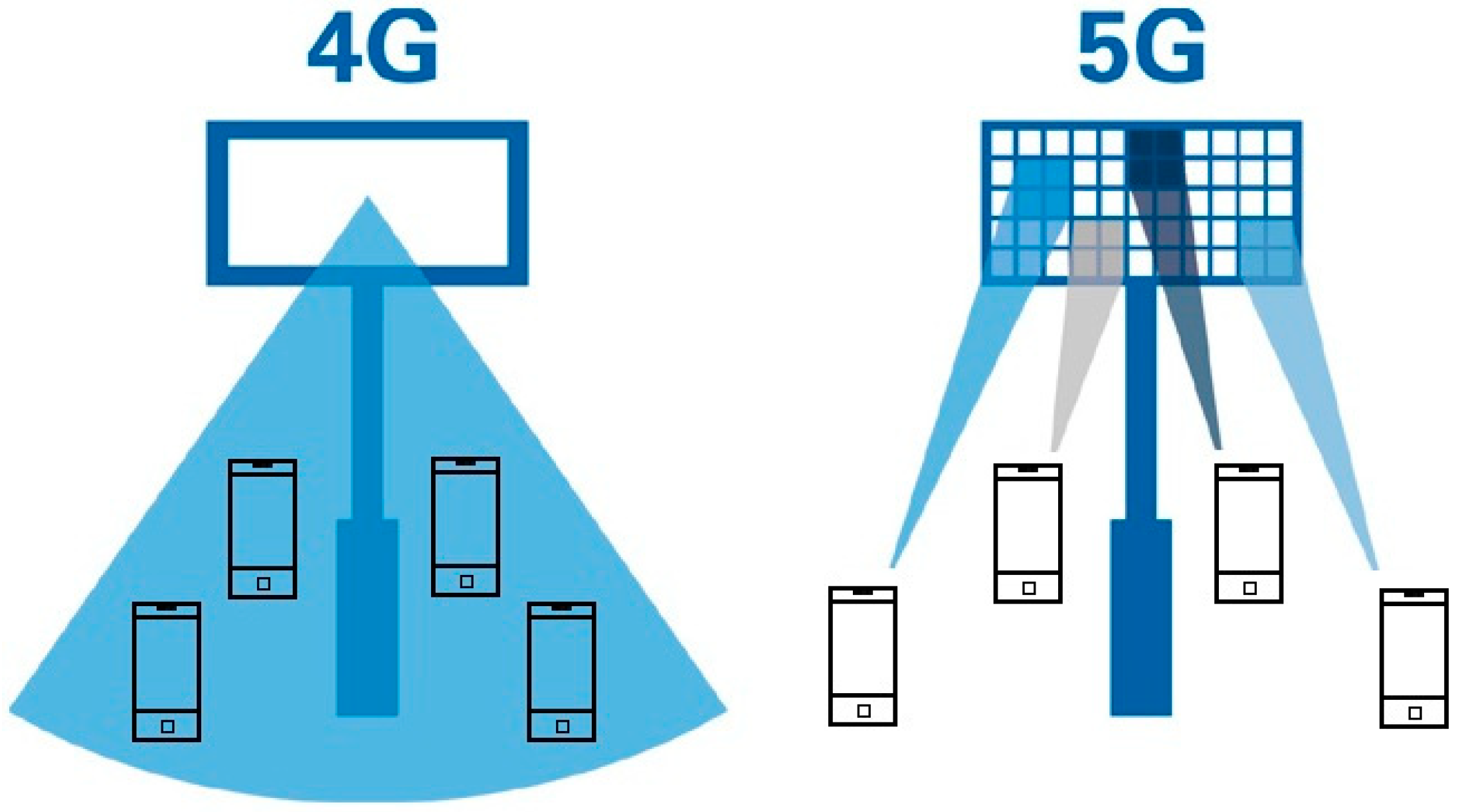
Figure 1. Conventional 4G and 5G antenna systems.
Symmetry 12 01167 g001
Figure 2. Design of the multichannel symmetry transmit RF front-end.
Symmetry 12 01167 g002
Figure 3. Photo of one-channel single-chip transmit RF front-end (RFFE) monolithic microwave integrated circuit (MMIC).
Symmetry 12 01167 g003
Figure 4. Electrical scheme of the 180 and 90° bits of the phase shifter.
Symmetry 12 01167 g004
Figure 5. Layout plot of the 180 (a) and 90° (b) bits of the phase shifter.
Symmetry 12 01167 g005
Figure 6. Electrical scheme of the 45 and 22.5° bits of the phase shifter.
Symmetry 12 01167 g006
Figure 7. Layout plot of the 45 (a) and 22.5° (b) bits of the phase shifter.
Symmetry 12 01167 g007
Figure 8. Electrical scheme of the 11.25 and 5.625° bits of the phase shifter.
Symmetry 12 01167 g008
Figure 9. Layout plot of the 11.25 (a) and 5.625° (b) bits of the phase shifter.
Symmetry 12 01167 g009
Figure 10. Layout plot of the three stages of the power amplifier (a) and the Lange quadrature coupler (b).
Symmetry 12 01167 g010
Figure 11. Dependences of output power density and cutoff frequency on the gate width of the 0.25 µm GaAs pHEMT.
Symmetry 12 01167 g011
Figure 12. Phase shift versus frequency of the single-chip RF front-end MMIC.
Symmetry 12 01167 g012
Figure 13. Dependence of RMS phase shift error of the single-chip RF front-end MMIC on the frequency.
Symmetry 12 01167 g013
Figure 14. Dependence of gain of the single-chip RF front-end MMIC on the frequency.
Symmetry 12 01167 g014
Figure 15. Dependence of RMS gain error of the single-chip RF front-end MMIC on the frequency.
Symmetry 12 01167 g015
Figure 16. Dependence of output power (P-3dB) at the 0° phase state of the single-chip RF front-end MMIC on the frequency.
Symmetry 12 01167 g016
Figure 17. Dependence of PAE at 1 dB gain compression at the 0° phase state of the single-chip RF front-end MMIC on the frequency.
Symmetry 12 01167 g017
Table 1. State-of-the-art single-chip transmit RFFE MMICs.
This WorkRef. [14]
ParameterMinMaxMinMaxUnits
Frequency27.528.3527.528.35GHz
RMS Phase Error 3 2.38deg.
RMS Gain Error 0.63 0.23dB
Gain20.021.320.521.5dB
P1dB at 0°--29.830.2dBm
P3dB at 0°28.729.0--dBm
PAE at P1dB at 0°19.219.32324.2%