Abstract
Transition metal functional oxides, e.g., perovskite manganites, with strong electron, spin and lattice correlations, are well-known for different phase transitions and field-induced colossal effects at the phase transition. Recently, the interfaces between dissimilar perovskites were shown to be a promising concept for the search of emerging phases with novel functionalities. We demonstrate that the properties of manganite films are effectively controlled by low dimensional emerging phases at intrinsic and extrinsic interfaces and appeared as a result of symmetry breaking. The examples include correlated Jahn–Teller polarons in the phase-separated (La1−yPry)0.7Ca0.3MnO3, electron-rich Jahn–Teller-distorted surface or “dead” layer in La0.7Sr0.3MnO3, electric-field-induced healing of “dead” layer as an origin of resistance switching effect, and high-TC ferromagnetic emerging phase at the SrMnO3/LaMnO3 interface in superlattices. These 2D polaronic phases with short-range electron, spin, and lattice reconstructions could be extremely sensitive to external fields, thus, providing a rational explanation of colossal effects in perovskite manganites.
1. Introduction
Complex transition metal oxides with perovskite structure possess strong electronic correlations and display coupled phase transitions, caused by the interplay of charge, spin, and lattice degrees of freedom. The general chemical formula of such materials is RE1−xAxTMO3 (RE = La, Pr, Nd, etc.; A = Ca, Ba, Sr, and TM = Mn, Co, N, Cu) and the typical representative are the so-called manganites, nickelates, cobaltates, cuprates and “double perovskites”, e.g., La2CoMnO6. For doped manganites, such as La1−xSrxMnO3, electronic correlations, being more or less strongly coupled to the lattice (phonons), drive a ferro-paramagnetic (FM-PM), PM-antiferromagnetic (AFM), metal–insulator (MI) and structural phase transition depending on the material composition [1,2]. These phase transitions have been summarized in rich phase diagrams with a number of thermodynamically stable phases, such as FMM, PMI, AFMI [3,4,5]. In addition, the spin-ordered insulating phases can be charge and/or orbital ordered (COO) at low temperatures. It is due to the phase transitions and strong spin–spin, spin–phonon, and electron–phonon couplings that strongly correlated oxides display drastic changes in electrical resistivity, called as colossal magnetoresistance [6,7] (CMR) as well as in optical and elastic properties, dubbed “colossal magnetorefractive” [8] and “colossal magnetoelastic” [9] effects, respectively.
Furthermore, strongly correlated oxides with Mn, Cu or Ti at B-sites are inclined to a structural instability, called Jahn–Teller (JT) effect [10]. This leads to the formation of the so called JT correlated polarons [11] or bipolarons [12] and results in the localization of charge carriers by means of lattice distortions additionally enhanced by a random distribution of A-site cations, e.g., La3+ and Ca2+. Remarkably, electronic properties of manganites with strong electron–phonon coupling, i.e., (La1−yPry)0.7Ca0.3MnO3, can be spatially inhomogeneous: They possess a unique phenomenon nanoscale electronic phase separation, the evidence for which was demonstrated experimentally [13,14] and studied theoretically [15,16]. A direct relation between the phase separation and colossal magnetoresistance was also shown in the earlier reports.
A rich diversity of functionalities based on the involved charge, spin, and lattice degrees of freedom is the hallmark of strongly correlated oxides, also called functional oxides. They possess technologically important properties, such as (a) high-TC superconductivity, e.g., YBa2Cu3O7−δ (YBCO) with transition temperature, TC~90 K; (b) ferroelectricity, e.g., Pb(Zr,Ti)O3 (PZT), with high remnant electrical polarization, p~100 μC/cm2, and high Curie temperature, TC~500 K; (c) a half-metallic ferromagnetism in doped manganites, e.g., (La,Sr)MnO3, with relatively high TC = 370 K; and (d) multiferroic behavior in BiFeO3 with coexisting magnetic (G-type AFM) and ferroelectric order parameters at room temperature [17]. All these properties are promising for future emerging technologies, especially for magnetic- and resistive-random access memories (MRAM and RRAM). Conceptually new multiferroic devices with electrically/elastically coupled ferromagnetic and ferroelectric counterparts cross-controlled by electric and magnetic fields were conceived based on the magnetoelectric and multiferroic effects.
All this underscores a great scientific and technological interest in thin films and heterostructures of correlated oxides. Considering fundamental problems of known semiconducting materials at the nanoscale, i.e., strong fluctuations in the distribution of dopants and the fact that quantum confinement dominates already at the 100 nm scale [18], the oxide films could play an important role in the next generation of electronics (oxytronics) and in the nanoscience. Recent successes in the thin film growth technologies demonstrated their extreme precision and advantages for the study and control of electronic correlations down to the atomic scale. As a result, a promising research avenue appeared in the last few years with the main goal to search for interfacial emergent phases (EP) in perovskite heterostructures. EPs reveal an unusual electronic behavior, which could not be observed in the constituent layers. The most prominent example is a metallic EP between two insulators LaAlO3 (LAO) and SrTiO3 (STO), i.e., the LAO/STO interface [19]. Generally, the EPs, are confined within a very narrow interfacial region of 1 to 2 unit cells (u.c.) and can be treated as two dimensional (2D) phases, the properties of which are less dependent on the thickness of the constituting layers. A fundamentally interesting aspect of heterostructures is that they allow to search for new symmetry-breaking-induced phases at the interfaces, where dimensional confinement, strain, chemical interactions, topological singularities, and discontinuities of the electromagnetic field/potential can take place [20]. All these ingredients contribute to insulator–metal transitions, magnetism, and superconductivity, [21,22,23,24] observed for EPs.
However, there is an essential bottleneck on the way to understanding the correlation physics and to practically implementing strongly correlated oxides. Namely, doped or isovalent-cation-substituted manganites, e.g., (La1−yPry)0.7Ca0.3MnO3 (LPCMO) are multicomponent compounds and, thus, they are prone to the chemical (substitutional) disorder [25]. Such “quenched disorder” was even considered to be an unavoidable problem of manganites and correlation physics as well, because both “filling” (FC) and/or “bandwidth” (BC) control tactics [26] of the parent Mott insulator, e.g., LaMnO3, can lead to random distributions of electrostatic (Coulomb) and elastic (strain) fields due to the difference of valence state (La3+ and Ca2+) and size (La3+ and Pr3+) of A-site cations. As a result, the mobility of itinerant charge carriers additionally decreases (Anderson localization), yielding a hopping transport. This is another important reason why the layered architecture of perovskite films in heterostructures, in addition to the opportunity to search for EPs, could be promising to suppress the cation disorder.
The motivation for this review article was to summarize our recent results, about the search for new low dimensional (nanoscale) emergent phases in manganite films and superlattices. Special attention was paid to further development of the metalorganic aerosol deposition (MAD) [27] along the improvement of growth accuracy down to 1 monolayer of growing film and elaboration of an in situ growth control using optical ellipsometry [28,29]. Our results are concentrated along two main research lines: (a) intrinsic JT polaronic nanophases located at the surface and in the volume of phase-separated CMR manganites and (b) artificial nanoscale EPs, induced by applied voltage pulses, or static EPs located at the interfaces in perovskite superlattices. By using Raman, surface- and tip-enhanced Raman (SERS and TERS) spectroscopy we have directly demonstrated that the CMR effect is related to the magnetic-field-induced suppression of JT polaronic nanophases [30,31]; in this sense, it could also be called the colossal magneto–phononic effect. By applying SERS, we observed such phases at the surface of a manganite [32] because of the symmetry-break-induced electronic reconstruction, theoretically predicted by Calderon et al. [33]. The importance and novelty of artificial nanoscale EPs is highlighted by the observations of (1) a high-TC ferromagnetic EP at the SrMnO3(top)/LaMnO3(bottom) (SMO/LMO) interface [34] caused by the electron transfer from the LMO “donor” layer into the SMO “acceptor” layer, and (2) the electric-field-induced resistance switching in the layer-by-layer fashion [35] of electrically highly isolated “dead layer” at the La0.7Sr0.3MnO3 (LSMO) surface and formation of the embedded conducting layers, which allow a robust multi-state memristive functionality.
2. Experimental Techniques
2.1. Metalorganic Aerosol Deposition (MAD) Technique
The MAD technique was originally developed to grow epitaxial films of high-TC superconductors YBa2Cu3O7−x [36]. Later on, other functional oxides, such as manganites, cobaltates, titanites, ruthenates, manganite/titanite superlattices, and nanocomposite films [22,37,38,39,40,41,42], as well as single-oxide films of ZnO, MgO, Al2O3, have been successfully obtained by MAD. The essence of a vacuum-free MAD, operating at a high partial pressure of oxygen, pO2~0.2 bar, is the use of aerosols of solutions of metalorganic precursors, containing all necessary chemical ingredients, e.g., La-, Ca- and Mn-acetylacetonates, in a molecular form. The precursor solution is sprayed using a pneumatic nozzle onto a heated substrate, Tsub = 400–900 °C, by using a compressed spraying gas (air or oxygen). An oxide film grows as a result of a heterogeneous pyrolysis reaction at the substrate surface in an oxygen-containing gas media. A high-temperature gradient close to the substrate leads to the formation of a dense mixed phase with coexisting liquid, vapor, and solid fractions in a very narrow “stagnation” region ≤1 mm over the substrate surface. This high-temperature “precursor phase” is the hallmark of MAD: The growth here deviates strongly from the non-equilibrium growth in physical (PVD) and chemical (CVD) vapor deposition and approaches an equilibrium growth similar to that in a liquid phase epitaxy (LPE). The advantage is a drastic decrease in the temperature-dependent supersaturation degree, α, and a concomitant increase in the nucleation cluster size, rS ~ 1/α [43,44]. As a result, the MAD growth conditions allow one to obtain epitaxial oxide films, nanocomposites, and heterostructures of high crystalline quality and perfect surface morphology [37,38,41].
In Figure 1 we present the scheme of the advanced MAD apparatus [28], which was developed recently with the main aim of improving growth precision. A specially designed pneumatic nozzle with up to 6 liquid channels is supplied by a SyrDos liquid dosing units (HiTec Zang GmbH). The precursor volume was controlled with accuracy, δV = 0.1 μL, which corresponds to a layer with the thickness ≈ 10−2 u.c. The film growth can be monitored in situ using an optical ellipsometry setup of polarizer–modulator-sample-analyzer (PMSA) type [45]. The complex reflection coefficient, ρ = rp/rs = tanψ × eiΔ, of a linearly polarized He–Ne laser beam (λ = 632.8 nm) at the Brewster incidence angle, θB(STO) = 62°, was measured using a lock-in-technique on ω = 50 kHz and 2ω = 100 kHz, frequencies. The phase shift, Δ, between the parallel (p-) and perpendicular (s-) component of the reflected beam, was calculated as Δ = arctan(Iω/I2ω) [45]; here Iω and I2ω are the measured intensities of the reflected light. The ellipsometric signal at an angle of incidence θB, being extremely sensitive [45] to the changes of the film’s optical properties, is used for the in situ growth monitoring of semiconducting AIIIBV films [46,47] within metalorganic chemical vapor deposition (MOCVD). Since MAD is a vacuum-free technique, the optical ellipsometry provides a unique possibility for in situ growth control. Note, the reflection high-energy electron diffraction (RHEED) technique can operate at very low pO2 < 1 mbar in pulsed laser deposition (PLD) and molecular beam epitaxy (MBE) setups.
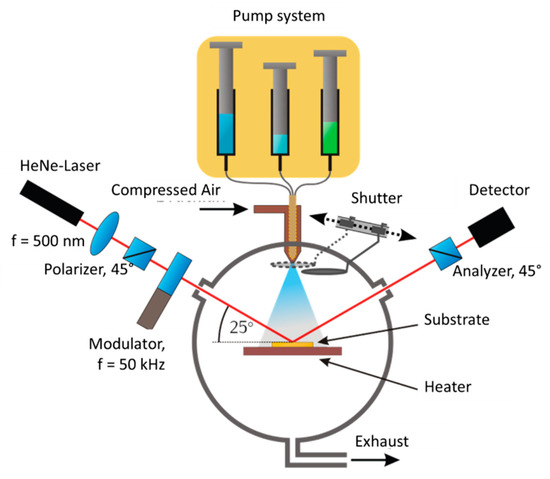
Figure 1.
The scheme of the metalorganic aerosol deposition (MAD) apparatus equipped with a precision liquid pump system and in situ growth monitoring by means of optical ellipsometry. Reproduced from [28] with the permission of AIP Publishing.
Ellipsometry monitoring during the MAD growth of 5 nm thick LSMO/STO(100) film is shown in Figure 2. After overcoming a transition region with a thickness D0 ~ 3 u.c. close to the STO substrate, a linear time dependence Δ(t) was observed in agreement with a constant growth rate, v =4.8 nm/min. The Δ(t) behavior can be renormalized into a thickness dependence as Δ = A*(v*t) = A*D and the phase shift rate, ALSMO = dΔ/dD ≈ 0.32°/u.c., was found to be constant during the growth, reflecting the constant optical properties of a homogeneously doped LSMO film with constant electronic density, N = 1 − x. Thus, the ellipsometric phase shift rate, dΔ/dD, is assumed to be a probe of the charge density/u.c. or, in case of (LMO)m/(SMO)n superlattices34 of the averaged doping level, x = n/(m + n) in superlattices (SLs) (see Section 3.3 below).
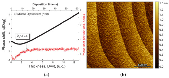
Figure 2.
(a) The time dependence of the phase shift angle, Δ(t), during the growth of a 5 nm thick La0.7Sr0.3MnO3/SrTiO3 (LSMO/STO) (100) film. After overcoming a transition region of D0 ≈ 3 u.c., a linear increase in Δ with time is evident in agreement with a constant deposition rate, v ≈ 4.8 nm/min. “Reprinted figure from [34] under permission licensed by John Wiley and Sons (Nr. 4654230253827)”; (b) paramagnetic-antiferromagnetic (AFM) image of epitaxial LSMO/STO(100) film reveals a layer-by-layer growth with one atomic layer height terraces and mean square roughness, RMS = 0.2 nm.
The currently developed MAD was shown to be successful in preparation of various oxide films and heterostructures of correlated oxides with very high crystalline quality. Moreover, B-site ordered double perovskite films, e.g., RE2CoMnO6 (RE = La, Pr, Nd, etc.), with perfect crystallinity and a high degree of B-site ordering ~98% were obtained [48,49,50]. In addition, we have demonstrated the growth of intrinsically layered Ruddlesden–Popper heterostructures, e.g., SrO(SrTiO3)n (n = 1–4), by means of the atomic layer epitaxy [28,29] (ALE); this type of growth has been realized earlier only by means of MBE [51]. All this demonstrates that MAD with the growth control down to 1 monolayer has a great potential for oxide films and heterostructures.
2.2. Raman Spectroscopy
Since the discovery of high-TC superconductivity in cuprates [52], Raman spectroscopy has been shown to be a powerful and nondestructive method to study the structure and electron–phonon coupling in strongly correlated oxides. Numerous Raman studies on doped manganites, performed up to now, focused on the relationships between the structure, chemical composition, and temperature [53,54,55,56,57,58,59]. Moreover, Iliev et al. [60] addressed the JT disorder due to the statistical distribution of Mn3+ and Mn4+ caused by doping. They have shown that Raman spectra reflect unambiguously the structural disorder induced by short-range JT distortions, which vary with doping level and temperature. The difference between the Raman spectra of the JT disordered LPCMO film [30] and of the cation ordered La2CoMnO6 (LCMO) film [48,49] is shown in Figure 3. One can clearly see that LPCMO (Figure 3a) with stochastically distributed Mn3+/Mn4+ ions due to Ca-doping display weak and very broad two Raman bands with FWHM~100 cm−1, which can be fitted by Gauss functions. These bands originate from the antistretching (A2g around 490 cm−1) and stretching (B2g around 614 cm−1) JT vibrations of MnO6 octahedra. In addition, one can also see a sharp bending mode (B2g around 440 cm−1). In contrast, the Raman spectrum of a B-site ordered double perovskite film LCMO (Figure 3b) with only Co2+ and Mn4+ ions [48] (they both are not JT ions) and without JT disorder is composed of narrow and strong Raman phonon modes (Ag breathing and B1g combined modes around 640 cm−1 and 480 cm−1, respectively) with FWHM~30 cm−1, which can be nicely fitted by Lorenz functions.
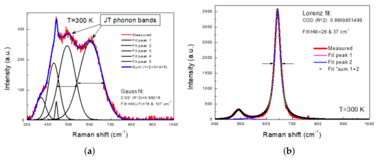
Figure 3.
Raman spectra of a typical colossal magnetoresistance (CMR) manganite (La1−yPry)0.7Ca0.3MnO3 film (a) and of a B-site ordered double perovskite film La2CoMnO6; and (b) measured at room temperature by using a second harmonic of Nd:YAG laser excitation with λ = 532 nm.
To study the JT correlated polaronic phases, we applied additionally to normal Raman spectroscopy the Tip-(TERS) [61] and surface-enhanced-Raman spectroscopy [32] (SERS). These techniques, both based on the enhancement of electric field close to a metallic surface, i.e., Au tip in TERS and Au nanoparticles in SERS, by surface plasmons, allow one to significantly increase the Raman cross-section and, thus, to “visualize” lattice vibrations (phonons) at the film surface. TERS and SERS are widely used for studies of biomolecules as they allow an ultimate high sensitivity down to the single molecule. However, SERS and TERS have been rarely applied to study surfaces of thin solid films.
3. Emergent Phases in Manganite Films and Superlattices
3.1. Polaronic EPs at the Internal Interfaces in the Phase Separated LPCMO
We have studied the classical CMR manganite–LPCMO (y = 0.4) films [30,31] heteroepitaxially grown on MgO(100) in a strain-free state by the MAD technique. Complex measurements of magnetization, linear and nonlinear electrical resistance, as well as Raman spectroscopy, were carried out to monitor the temperature- and magnetic field-driven development of JT correlated polarons (see Figure 4). The main result is that CMR in the phase separation regime for 180 K < TC < 220 K originates from a peculiar magnetic/electric state with FM nano-domains with averaged radius, RFM ~ 6–8 nm, AFM coupled by correlated JT polarons (CPs). The anomalous increase in the coercive field by approaching TC from below in Figure 4 evidences the enhancement of AFM coupling. The concentration of polarons, estimated from the nonlinear electrical resistance (see Figure 4), increases steeply to a value nCP ~ 0.5% as the temperature approaches TC.
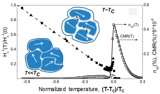
Figure 4.
Normalized coercive field, Hc(T)/Hc(0) (left scale), concentration of correlated polarons, nCP in percent (open squares) and colossal magnetoresistance, CMR × 5 × 10⁻⁶ (line), in two (La1−yPry)0.7Ca0.3MnO3 (LPCMO)/MgO(100) films with different Pr-substitution (y = 0.375 and 0.4) as a function of the normalized temperature, (T−TC)/TC, because the films have different TC values, i.e., 195 K (y = 0.4) and 210 K (y = 0.375). Closed squares and triangles depict the Hc(T) ~ T1/2 behavior for films with Pr concentration y = 0.375 and 0.4, respectively. An anomalous increase in the coercive field close to TC indicates the enhancement of AFM coupling in the phase-separated state. “Reprinted figure with permission from [30] Copyright (2014) by the American Physical Society”.
This agrees nicely with the increase in the intensity of JT bands in the vicinity of TC, observed by the temperature-dependent Raman spectroscopy shown in Figure 5. As the film undergoes an FM phase transition, the intensity of JT phonon bands (ωs) gets suppressed, and the intensity of the bending mode (ωbend) starts to grow in the FMM state.
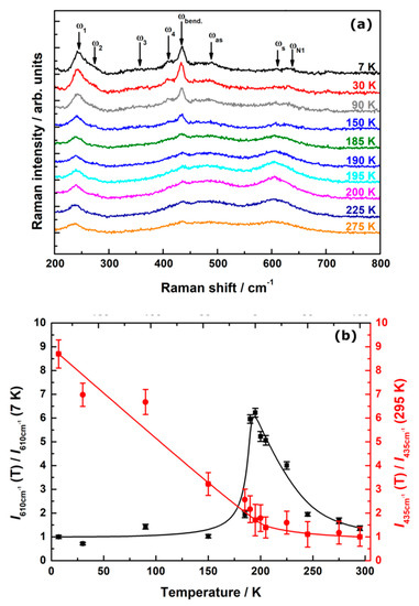
Figure 5.
(a) Raman spectra of an LPMCMO/MgO(100) film (y = 0.4) measured in the temperature range 7to 300 K; and (b) Normalized intensity of the JT phonon band (ωs) I610 cm−1 and of the bending mode (ωbend) as a function of temperature. “Reprinted figure from [31]. Licensed under the Creative Commons Attribution 4.0 International License, http://creativecommons.org/licenses/by/4.0/”.
The ultimate evidence for the decisive role of correlated polarons in CMR was obtained by magnetic-field-dependent Raman spectroscopy. As one can see in Figure 6, the applied field close to TC suppresses the JT phonon bands or, in other words, the JT disorder in the MnO6 network. Simultaneously, the lattice order, described by the enhancement of the bending phonon mode (ωbend), increases. Far below and far above TC, no effect of the magnetic field on Raman spectra was detected in remarkable analogy to the minor resistance changes in the magnetic field for T << TC and T >> TC seen in Figure 4. Note, that even quantitative agreement between the calculated values of CMR = 100% × (R(0) − R(5T))/R(5T) = 7000% and the magnetic-field-induced suppression of the intensity of JT phonon band (ωs), 100% × (I(0) − I(5T))/I(5T) = (6–9) × 103 was obtained [31], unambiguously evidencing the decisive role of JT correlated polarons in CMR.
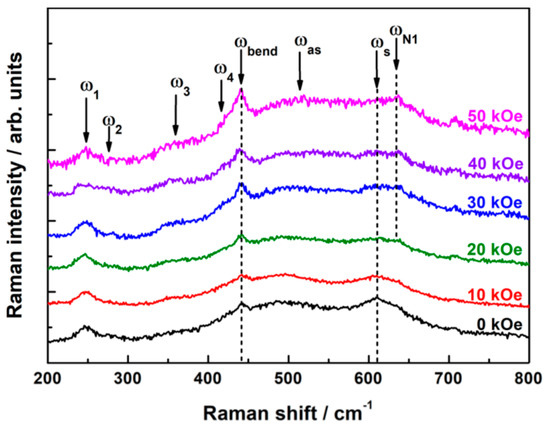
Figure 6.
Raman spectra of an LPCMO/MgO film measured close to TC = 197 K at different applied external fields, H = 0–50 kOe. “Reprinted figure from [31]. Licensed under the Creative Commons Attribution 4.0 International License, http://creativecommons.org/licenses/by/4.0/”.
We modeled the magnetic structure (see the sketch in Figure 4) within the phase separation scenario [15] as an assembly of single-domain ferromagnetic nanoparticles, antiferromagnetically coupled (pinned) by correlated JT polarons (CPs) located at the domain walls. CPs as short-range-ordered lattice superstructures with correlation length δ ~ 1–2 nm and charge/orbital ordering (COO) of CE type were detected previously in neutron and x-ray scattering [62,63,64,65]. A preferred formation of the insulating COO phase at two-dimensional defects, such as surfaces and interfaces, is well documented in the literature [40,66,67] and can be understood by assuming a weakening of the concurring FM double exchange at defects. Phenomenological Ginzburg–Landau approaches predict the formation of a charge-ordered [68] and AFM state [69] within the domain wall, especially when the bulk (domain) phase is located not far away from the FM/AFM boundary in the phase diagram [5]. This is exactly the case for our LPCMO, which is bandwidth controlled by Pr substitution to be close [70] but not crossing the FMM/AFMI phase boundary, which lies at y ~ 0.6–0.7 [71]. A nice correspondence between generic theoretical phase diagram [5] and experimental data [70] on optimally doped strain-free manganite films with different Goldschmidt tolerance factor1, t = (rA + rB)/√2(rB + rO) was obtained assuming the electron–phonon coupling constant, λ, scales with the deviation of the perovskite structure from the cubic one with t = 1, i.e., λ ~ 1−t. Thus, domain walls in LPCMO provide a unique intrinsic possibility to host CPs, which then possess short-range AFM correlations in agreement with the AFM ground state of the CE phase.
As a result, a peculiar low-field CMR behavior with magnetic hysteresis and slow resistance relaxation, both induced by the magnetization reversal, was observed in the phase-separated (mixed) state [30]. The T-scale for the mixed state and the underlying AFM coupling in LPCMO is limited from above by the appearance of charge ordering at TCO ∼ 220–230 K [13,31], which breaks the high symmetry of the PM phase and enhances the formation of CPs. Within the narrow temperature interval, 180 K < TC < TCO, a mixed phase with AFM layers and coupled FM nanodomains exists, yielding extremely large field-induced changes in the resistance and in the Raman spectra, accompanied by a metamagnetic transition [30]. If a manganite undergoes FM transition above TCO, such as optimally doped La0.7Ca0.3MnO3 with TC ~ 260 K, a much moderated CMR ~ 400% can be observed because the concentration of CPs [30] in LCMO, nCP ~ 10−4%, is much lower than that in LPCMO. It is worth noting, a very small CMR~30%, observed in a classical double exchange material La0.7Sr0.3MnO3 with rhombohedral (R-3c) structure, is explained by the absence of CPs simply because this structure is not compatible with static JT distortions.
Summarizing, the small size of FM nanodomains, RFM ∼ 6–8 nm, in compositionally tuned LPCMO with relatively strong electron–phonon coupling taken together with the estimated coupling constant, JAFM = 4.5 × 10⁴ J/m2, provide a rational solution of the long-standing issue in CMR physics, i.e., how a tiny amount of CPs can be responsible for extremely large magnetic-field-induced changes in electrical resistance. Note, that colossal effects are not limited to CMR, very large and hysteretic field-induced changes of refractive index [8] and of the elastic moduli [9] were also observed in LPCMO.
3.2. EPs at the Surface of Manganite Films
3.2.1. Symmetry Breaking Effect
Considering the above mentioned preferable nucleation of correlated JT polarons at 2D defects, one can suggest the surface of a manganite can also host CPs. Moreover, we can correlate the CPs at the surface with a well-known problem of the so-called “dead layer” (DL) at the surface and/or at the interface manganite/substrate. A non-ferromagnetic and insulating DL at the surface of manganite films was observed by conducting atomic force microscopy [72,73], x-ray magnetic circular dichroism (XMCD) [74] on La0.7Ca0.3MnO3 (LCMO) and by x-ray resonant magnetic scattering (XRMS) [75,76] on La0.7Sr0.3MnO3 (LSMO). The DL behavior, being in strong contrast to the FMM ground state in the volume of a manganite film, points out to a symmetry-break-induced electronic and structural reconstruction at the manganite surface. According to earlier theoretical models, the surface (DL) was predicted to be electronically-rich [33] or to show a peculiar 2D structure of CE type, which is similar to that found in half-doped manganites [66].
As we have shown very recently [32] the SERS technique with its high sensitivity can be applied for the study of real surfaces of LSMO and LCMO films. To do this, we have elaborated a simple way to deposit Au-nanoparticles (Au-NPs) on the surface of a film by using the MAD technique [77]. High pO2 ~ 0.2 bar within MAD allows one to prevent deoxygenation of the manganite surface while deposition of Au-NPs, thus, keeping the surface intact. As a result, magnetic and electric properties of ultrathin LSMO/STO(001) films with a thickness of 12 u.c. remain the same before and after the deposition of Au-NPs (see Figure 7). A scanning electron microscopy image in the inset of Figure 7 indicates a homogeneous covering of Au-NPs with a rather broad particle size distribution, commonly observed for aerosol- or vapor-based nanoparticle growth [78,79]. A mean particle size of dAu~16 nm was obtained.
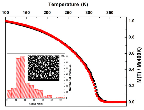
Figure 7.
Temperature dependence of the normalized magnetization, M(T)/M(400 K) of a 12 u.c. thick LSMO/STO(100) film before (black) and after (red) deposition of Au-nanoparticles (Au-NPs). The inset shows particle size distribution calculated over the shown secondary electron microscopy image. “Reprinted figure from [32]. Licensed under the Creative Commons Attribution 4.0 International License, http://creativecommons.org/licenses/by/4.0/”.
The usual (bulk) Raman spectrum and SERS of an LSMO/MgO(200) film are presented in Figure 8a,b, respectively. The important lines in the “bulk” spectrum of LSMO relate to the rotational (178 cm−1, A1g) and bending (422 cm−1, Eg) modes in agreement with previous reports [80,81] and lattice dynamics calculations [82]. Additional, forbidden in the R-3c structure of LSMO [82,83], weak “orthorhombic” contributions at 331 and 396 cm−1 and the JT modes at 470 and 630 cm−1 were also observed. The probable reason is the existence of small orthorhombic distortion at the film/substrate interface [84,85] due to strain-releasing misfit dislocations within the first ≈ 2 nm from the interface [86]. After overcoming this defect- and strain-rich region the film grows strain- and almost defect-free [37] with the pseudocubic lattice constant, Cfilm = 3.882 Å, very close to the bulk value.
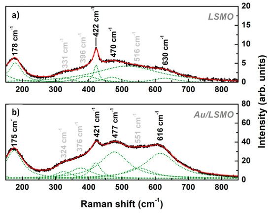
Figure 8.
(a) Raman “bulk”; and (b) surface-enhanced Raman spectroscopy (SERS) spectra of an LSMO/MgO film with thickness d = 89 nm. [32]. Licensed under the Creative Commons Attribution 4.0 International License, http://creativecommons.org/licenses/by/4.0/”.
A broad feature with a maximum at ~515 cm−1 corresponds to a collective plasma-like excitation in LSMO [58]. The SERS of LSMO, shown in Figure 8b reveals a strong enhancement of the JT bands at 477 and 616 cm−1, i.e., the SERS contrast ISERS/IRaman = 31–34, compared to the relatively weak enhancement of the rotational and bending mode ISERS/IRaman = 7. The enhancement cannot be caused by the film/substrate interface since the surface plasmon electric field decays very fast within the film body. Considering the film thickness, dfilm = 89 nm, and the distance dependence of the plasmonic enhancement [87], I(r)~1/r10, the enhancement contribution from the film/substrate interface would be only ~10−8 compared to that of the surface. Thus, the observed enhancement of the JT modes in the SERS of LSMO is definitely a surface phenomenon.
We have argued [32] the appearance of the JT-like modes at the LSMO surface is an electronically driven intrinsic process directed to compensate the electrostatic mismatch at the film/vacuum interface. This proceeds by means of a charge transfer from the film volume to the surface and leads to the formation of an insulating Mn3+-rich surface layer in accordance with the earlier theoretical model of Calderon et al. [33]. As a consequence, the crystal structure at the surface of LSMO changes from the rhombohedral (R3c) in bulk the orthorhombic (Pnma) structure [88], which is compatible with the JT modes. In addition, we assume that the enhancement of the Mn3+/Mn4+ disorder in octahedral network yields to a highly insulating surface layer called the dead layer.
To model the surface structure of LSMO, we compared the intensity contrasts of the different modes. Considering the 1/r10 distance dependence of the plasmonic enhancement [87], the significantly higher SERS contrast of JT modes compared to the bending mode is directly related to a stronger JT surface contribution. The bending mode can be considered as a bulk-like mode and can be used to estimate the thickness of the JT-distorted surface layer. Using the simplified sphere model, the SERS intensity shows a distance dependence [87] ISERS ∼ [(1 + r/a)]−10, shown in Figure 9. Here ISERS is the SERS intensity of the Raman mode, a is the curvature radius of the field enhancing Au surface, approximated by the mean particle size dNP ≈ 16 nm, and r the distance from the metallic surface to the adsorbate. Since the bending mode is treated as a bulk mode, the determined ratio η = Cbend/CJT ≈ 7/31 represents the weakening of plasmonic enhancement within the distorted surface layer. Its thickness can be estimated from the dependence in Figure 9 by finding the distance, r, at which the η ≈ 7/31; this yields the thickness of LSMO surface layer, dJT ≈ 7 u.c. ≈ 2.7 nm. This value corresponds well to those obtained for the AFMI surface layer from XMCD [74] and XRMS [76].
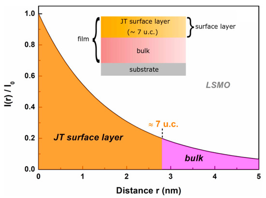
Figure 9.
The distance dependence of plasmonic enhancement and the estimated thickness of the surface layer in LSMO. The inset shows the proposed model of the surface layer. [32]. “Licensed under the Creative Commons Attribution 4.0 International License, http://creativecommons.org/licenses/by/4.0/”.
3.2.2. Electric Field Effect
Electric-field-driven resistive switching, being widely spread phenomenon in heterostructures of correlated oxides, including perovskite manganites, [89,90,91] was believed to be promising for novel multistate resistive memory (memristive) applications including advanced neuromorphic computing [73,92,93]. Recently [35] we have demonstrated that a multistate functionality can be obtained in an intrinsic heterostructure, comprising the “dead layer” (DL) at the surface of a manganite film. The DL acting as a tunneling barrier plays a most active role being electrically switchable in monolayer steps between two intrinsically well-defined resistance states.
The resistive switching behavior at the free surface of a heteroepitaxial La0.85Sr0.15MnO3/MgO film grown by MAD was analyzed by conductive atomic force microscopy (CAFM). Switching experiments were carried out at room temperature with an Omicron VT-AFM under UHV (< 3 × 10⁻¹⁰ mbar). Commercial Pt-coated probes from MikroMasch with a spring constant of 0.15 N/m were used. CAFM measurements were recorded at vertical force set points ≤ 5 nN, and all current maps were recorded at a positive tip bias of 0.1 V. CAFM scanning over the sample surface, accompanied by switching on a nanometer-scale and simultaneous recording of the topography and current maps, has proven indispensable for microscopic study of memristive effects [73,94,95,96,97,98]. Previously, we have shown that the surface of manganite epitaxial [73,98,99] and nanocolumnar [97] films initially exhibit a very high resistance state (HRS). It can be switched to a low resistive state (LRS) by applying a positive electric pulse voltage to the tip, U > 3 V, and back to HRS by applying a negative voltage pulse.
Beyond the previously reported switching characteristics, we observed discrete conductance levels on a microscopic scale. First, the LRS metal was initialized by several fast scans (1000 nm) under a positive electrical tip bias of 6 V; simultaneously recorded current maps confirmed the LRS on the entire scan area. Next, voltage pulses of reversed (negative) polarity, applied at four cantilever positions, yielded the emergence of two extended areas (see Figure 10a) of increased resistivity: (1) around the lower right pulse position and (2) including both upper pulse positions. Comparison with the topography data in Figure 10b, illustrated by line profiles of height and resistance in Figure 10d, reveals a remarkable correlation between the sample height and the magnitude of the discrete resistance levels: the regions of lower (higher) resistance are found primarily in shallow (protruding) regions, respectively. As the vertical length scale spans only a few lattice constants, we claim that the discrete current values stem from the insulating barriers with thicknesses of integer numbers of atomic layers. The intensity maps in Figure 10c suggest a nonrandom, logarithmic spacing of the possible current values, indicating the HRS acts as a tunnel barrier. Therefore, we ascribed the HRS levels to the existence of DLs induced by the symmetry break at the surface. Recent studies on LSMO elucidated the loss of inversion symmetry at the surface results in a preferential occupation of the out-of-plane 3z2 − r2 orbital and in the emergence of a C-type antiferromagnetic layer with a thickness of ≈ 2.4 nm [100,101]. Our results imply that both direct HRS-LRS (Utip > 0) and back LRS-HRS (Utip < 0) transformations proceed in a layer-by-layer fashion.
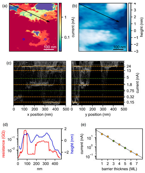
Figure 10.
(a) A current map recorded at U = 0.1 V after switching to the low resistive state (LRS) (red). Negative voltage pulses have been applied at the locations indicated by circles; (b) Corresponding topography image. The correlation between contact resistance (red) and height (blue) is illustrated by profiles along the indicated path (d); (c) Distribution of current values depending on the “x” and “y” locations as an intensity map. The identified logarithmically spaced current values are shown in orange (missing levels are indicated in green); and (e) Current as a function of the tunnel barrier thickness with a fit curve according to the Metal–Insulator–Metal model. “Reprinted figure with permission from [35] Copyright (2019) by the American Physical Society”.
According to our model [35], a dead layer at the surface, in contrast to the metallic LSMO in bulk, is viewed as a Mott–Hubbard insulator with a gap opening due to electronic correlations. Because of this gap, an intrinsic tunnel barrier is formed between the bottom (bulk metallic-like LSMO) and the top (Pt-coated AFM tip) electrodes. The width of this barrier and, thus, the tunneling conductance can be modified by electric fields. In this scenario, only two well-defined intrinsic resistive states are involved, and the observed multitude of “device” resistance levels (Figure 10c) originates solely from the varying number of layers, forming the insulating barrier at the surface. This picture is conceptually similar to that of switchable domain boundaries in multiferroic materials [101,102] and to the switching of ferroelectic and multiferroic tunnel junctions [103,104].
From the fitting of the current-thickness dependence in Figure 10e by the Simmons model [35] reasonable values for the minimum barrier thickness z0 ≈ 1.3 nm and the electrical contact area A ≈ 2.0 nm2 were obtained. The evaluated barrier height ϕ = 46 meV has to be considered as a rough estimate, but in any case, ϕ cannot exceed 60 meV. Thus, the observed exponential thickness dependence of the current and a convincing fit by the Simmons model both evidence a tunneling behavior in our CAFM measurements. Being remarkably small, this barrier height between bulk LSMO and the dead layer indicates a band bending and concomitant reduction of the bulk hole doping (x = 0.15) at the surface. While the minimal barrier thickness cannot be accurately determined from the given fit and some thickness values might be allowed yet unrealized in the presented experiments, it is yet remarkable that the obtained value of 1.3 nm is in perfect agreement a 2 to 4 u.c. thick very robust C-type antiferromagnetic layer at LSMO interfaces [99,100].
3.3. High-TC Ferromagnetic EP at SMO/LMO Interfaces
Perovskite heterostructures provide a rich playing field for design and engineering of oxide interfaces with the final goal to obtain interfacial EPs with unusual electronic behavior not present in the parent layers [105]. Recently we have reported [34] the MAD grown LaMnO3/SrMnO3 (LMO/SMO) superlattices (SLs), showing a ferromagnetic EP with Curie temperature TC≈ 360 K, originated from the electron transfer from the LMO “donor” layer to the overlying “acceptor” SMO layer. As a result, the SMO(top)/LMO(bottom) interface acquires ferromagnetic magnetization revealed by polarized neutron reflectometry.
The (LMO)m/(SMO)n superlattices (SLs) with integer number (m,n) of unit cells are artificial layered systems, in which the metal–insulator transition at TMI was found to depend on the m/n ratio [106,107,108]. The layered architecture allows diminishing the A-site disorder while keeping the averaged Sr-doping, x = n/(m+n), close to the optimal level, e.g., x = 1/3 for m = 2n. Such SLs have been usually grown by PLD and MBE. A bulk-like LSMO electrical and magnetic behavior was observed in SLs with very thin LMO and SMO layers, n = 1–2 u.c.; for n ≥ 3 an insulating ground state was established. In addition, an interfacial FM emergent phase with Curie temperature, TC ≈ 100–180 K, has been detected by polarized neutron scattering [107,108] and ascribed to the atomically sharp LMO/SMO interface. The rough reverse interface SMO/LMO did not contribute to the magnetic signal [109].
It is believed that EP formation is related to interfacial charge transfer [24,110], driven by the electrostatic (polar) mismatch. Some indications for the electronic/orbital interfacial reconstruction have been revealed by resonant soft X-ray scattering [106] and by linear/circular magnetic dichroism at the Mn L2,3-edge [19,111,112]. One can suggest that the charge transfer could be affected by the film growth conditions, such as temperature, oxygen partial pressure, epitaxy stress, etc. We have applied the MAD technique, providing high oxygen partial pressure pO2 ≈ 0.2 bar during deposition and equipped by in situ growth control by optical ellipsometry to study the EP formation in LMO/SMO SLs.
In Figure 11, we present the in situ measured time dependence of the ellipsometric phase shift ∆(t) during deposition of an [(LMO15/SMO5)]10 SL. One can see a different behavior during the growth of LMO and SMO layers. Namely, Δ(t) increases linearly by the LMO growth in agreement with an increase in the LMO thickness similar to the case of LSMO growth [34] (see also Figure 2). In contrast, the SMO layer displays a complex behavior clearly seen in the inset in Figure 11—the initial fast increase in Δ(t), followed by slowing it down at the end of SMO growth.
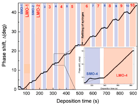
Figure 11.
Ellipsometric ∆(t) curve measured during deposition of an [(LMO15/SMO5)]10. The “blue”- and “red”-colored time intervals depict the SrMnO3 (SMO) and LaMnO3 (LMO) precursor pulses, respectively. During the delay time (“white”) between precursor pulses the ∆(t) does not change, indicating constant optical properties of the already grown layers. A zoomed view on the 4th (SMO/LMO) bilayer in the inset shows a nonmonotonous Δ(t) behavior during the SMO growth and a linear increase in Δ by the LMO deposition. “Reprinted figure from [34] under permission licensed by John Wiley and Sons (Nr. 4654230253827)”.
In Figure 12, we present a comparison between the temperature- and field-dependent magnetism in SLs and in LSMO and LMO single films grown on STO(001). The LSMO displays a classic double exchange ferromagnetism1 with TC = 355 K. The LMO film, in contrast to the A-AFM ground state in the stoichiometric bulk samples [1], reveals an FM behavior with TC = 160 K, stabilized probably by epitaxy strain [113] and stoichiometric oxygen concentration [114] provided by MAD. Remarkably, the M(T) curve (see Figure 12a,b) in SL with n = 5 reveals two well-separated transitions with TC1 < TC2, marking the low (LTP)- and high-temperature (HTP) FM phases, respectively. Moreover, the suppressed Msat(5 K) ≈ 1.3 μB/Mn, the increased Hc = 550 Oe, and a pronounced exchange bias field, HEB ≈ 100 Oe (see Figure 12b) point out the presence of an AFM phase at low temperatures.
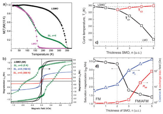
Figure 12.
(a) M(T) dependences with phase transitions at TC(LSMO) = 355 K and TC(LMO) ≈ 160 K and a two-phase behavior for a superlattice (SL) with n = 5; (b) M(H) curves measured at 5 K: LSMO (black curve, right scale) shows low coercivity and optimally large Msat = 3.6μB/Mn. SL with n = 5 reveals suppressed Msat = 1.3μB/Mn (olive), huge coercive field (Hc = 550 Oe) and a pronounced exchange bias field (HEB = 100 Oe). The high-TC FM phase in the SL is evidenced by the M(H) curve @ 300 K (red) and @ T = 160 K (blue); (c) Curie (TC) temperature behavior shows the emergence of a high-TC2 FM and reduction of TC1 for n > 2; (d) Increase in Hc and appearance of HEB accompanied by suppression of Msat illustrate a progressive AFM enhancement in SLs with n > 2. A phase boundary at n ≈ 2 separates a homogeneous FM and an FM/AFM phase coexistence in SLs. “Reprinted figure from [34] under permission licensed by John Wiley and Sons (Nr. 4654230253827)”.
We found the magnetism in SLs depends strongly on the thickness of the constituting SMO and LMO layers: SLs with very thin layers (n = 1,2) behave similar to a homogeneous LSMO film and for n > 3 an inhomogeneous AFM/FM behavior was observed (see Figure 12c,d). These data indicate that a boundary at ncr = 2 separates a homogeneous FM behavior (n ≤ 2) from a nonhomogeneous FM/AFM coexistence for SLs with n ≥ 3. As one can see in Figure 12c, TC1 decreases with increasing n and approaches TC ≈ 160 K for a single LMO film; we assigned it to the bulk-like LMO behavior. The enhanced AFM behavior for SLs n > 3 (see Figure 12d), is due to the SMO layer: It acquires the AFM character by increasing the thickness. Remarkably, the HTP for n > 3 reveals practically constant TC2 = 352–358 K, signaling a behavior typical for interfacial EPs [105].
The origin of the interfacial ferromagnetic EP can be obtained from the in situ growth monitoring by optical ellipsometry, superimposed onto the HRTEM HAADF image in Figure 13 (here the delays between SMO and LMO precursor pulses in the Δ(t) diagram were removed). One can see that the electronic properties of SMO in contrast to those of LMO are changing during the growth. Namely, the Δ-signal is additionally affected by the “electronic” parameter An(N, D), which reflects the changes in the electron density, N, within the first 2 u.c. of SMO growing on LMO. Here one can see a very large slope, dΔ/dD = An(N) ≈ 0.4°/u.c., which exceeds that for the following LMO layer ≈ 0.31°/u.c. This indicates an increase in the electronic density at the SMO(top)/LMO(bottom) interface. During the growth of the residual 3 u.c. of SMO, the phase shift rate decreases (Figure 13) leveling on the small value, An(N, D) ≈ 0.1°/u.c., in agreement with low electron concentration in SMO. The simulated the Δ(D) behavior (“green” curve in Figure 13, see also [29]) under the assumption of the electron transfer at the SMO/LMO interface fits nicely the measured Δ(D) behavior. Without charge transfer, the simulated “blue” curve (Figure 13) does not fit the measured one.
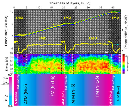
Figure 13.
Top panel: Phase shift Δ(D) (left scale) in SL n = 5, superimposed onto the HAADF HRTEM image. The experimental “yellow” curve is nicely reproduced by the simulated “green” one assuming an electron transfer within the first 2 u.c. of SMO. Without charge transfer, the simulated “cyan” curve does not fit the measured (“yellow”) one. The phase shift/unit cell (“yellow” curve, right scale), dΔ/dD, reflects the evolution of electron density in LMO/SMO layers. Middle panel: The 2D distribution of the electron-energy-loss spectra (EELS) of the O K edge structure for energies E = 532–537 eV along the growth direction shows the electron- (“yellow”) and hole-rich (“blue”) regions within the SMO and LMO layers, respectively. The EELS intensity increases from “blue” to “red”. Bottom panel: Qualitative model of the inhomogeneous electron density distribution along the growth direction: high-temperature (HTP) and low-temperature (LTP) ferromagnetic (FM) phases (“red” regions) are separated by two AFM phases: electron-rich (“red”) in SMO and hole-rich (“blue”) in the SMO and LMO. “Reprinted figure from [34] under permission licensed by John Wiley and Sons (Nr. 4654230253827)”.
A qualitative model of the charge distribution along the growth direction is shown in Figure 13 (bottom panel). Due to the electron transfer across the SMO/LMO interface, the SMO layers close to the interface acquire electrons, becoming quasi optimally doped and ferromagnetic in agreement with the phase diagram of Sr-doped LMO [4]. The electrostatic/polar mismatch between the SMO and LMO as the former possesses a shortage and the latter excess of electrons seems to be a driving force for charge transfer. It can be diminished by spreading the electrons into the SMO during growth. Another interface LMO(top)/SMO(bottom) is electronically sharp as the electrostatic mismatch between the LMO and vacuum drives electrons onto the surface of LMO. Our model agrees nicely with the theoretical predictions of Calderon et al. [33]. They pointed out an electron excess at the LSMO surface or in other words, an electron-rich and LMO-like surface termination. According to Figure 13, the characteristic scale of electron transfer ~ 2–3 u.c., explains clearly the existence of critical thickness ncr = 2 u.c., separating a homogeneous LSMO-like FM ground state (n ≤ 2) and inhomogeneous FM/AFM coexistence (n > 3).
4. Summary and Outlook
We wish to summarize this review on polaronic emergent phases (EPs) by pointing out the following important issues. First, an in situ growth control with a sub-monolayer sensitivity of thin films and heterostructures was demonstrated by MAD. Combined with different ex-situ characterization techniques (x-ray diffraction and x-ray reflectivity, transmission electron microscopy, atomic force microscopy, etc.), it allowed us to get electronic and structural information of film samples with the resolution down to atomic scale. Moreover, MAD specific growth conditions were shown to be advantageous for oxide films and superlattices.
Second, a remarkable similarity between polaronic emergent phases (EPs) of different types can be emphasized. Indeed, they all are low dimensional (2D) phases induced by broken symmetry of different types: (a) translational symmetry break at the surface yields to an electronic-rich and LMO-like JT-disordered insulating surface layer with a thickness of ~7 u.c. as detected by surface-enhanced Raman spectroscopy (SERS); (b) This dead layer can be additionally switched in a layer-by-layer fashion by an applied electric field; (c) inversion symmetry break at the SMO(top)/LMO(bottom) interface leads to an electron transfer and high-TC ferromagnetic interfacial 2 to 3 u.c. thick layer; and (d) the break of highly symmetrical paramagnetic phase due to charge ordering/localization leads to a JT correlated polaronic phase with a short-ordered charge and AFM spin correlations on a scale of ~1 to 2 nm. The concept of broken symmetry (translation and inversion) as an overarching theme for the appearance of emerging polaronic phases could be especially relevant for manganites containing cations with different valence, i.e., Mn3+/Mn4+.
Third, these 2D polaronic EPs are formed as a result of charge, spin, and lattice reconstructions at the interface with broken symmetry. Moreover, the reconstructed EPs were found to be extremely susceptible to applied external fields, e.g., electric, magnetic, temperature, strain, and, thus, can play a decisive role in colossal effects observed in perovskite manganites. Such high field sensitivity is probably caused by the 2D geometry of polaronic EPs and related to it a short-range-interaction between charge, spin, and phonon degrees of freedom, preventing the formation of long-range ordered phases.
Concerning the high-TC FM phase at the SMO/LMO interface, our interpretation is based mainly on the electrostatic/polar mismatch between LMO and SMO, assuming the absence of lattice relaxation effects in LMO, such as Jahn–Teller and tetragonal distortions. The study of lattice relaxations on the development of EPs seems to be a very interesting outlook topic as they should accompany the charge transfer according to the “electron–spin–phonon” paradigm of strongly correlated oxides; it will be considered in the near future.
Furthermore, an interesting and important avenue of research is the study and growth control of the so-called double perovskites, e.g., La2NiMnO6, promising ferromagnetic insulating materials for spintronic applications due to the magnetodielectric coupling and multiferroic behavior [49]. The structure of a double perovskite along the [111]-axis can be viewed as an infinite sequence of LaNiO3/LaMnO3 (LNO/LMO) layers. Considering the ionic formula of a B-site ordered double perovskite, e.g., La23+Ni2+Mn4+O62−, the B-site ordered phase differs from a disordered one by a charge transfer reaction: Mn3+ + Ni3+ → Mn4+ + Ni2+, i.e., an electron from Mn3+ will be transferred to Ni3+ ion. Analogously to the SMO/LMO interfaces, the B-site ordered phase can be viewed as an EP, appeared in, e.g., (LNO)m/(LMO)m superlattices, as a result of charge transfer. Such SLs provide a tool for ultimate control of B-site ordering by atomic layering.
Author Contributions
Conceptualization, V.M.; writing—original draft preparation, V.M.; writing—review and editing, V.M. and K.S.; project administration, K.S.
Funding
Financial supports from EU FP7 (IFOX project) and DFG (SFB 1073, TP B01, B04, A02) are acknowledged.
Acknowledgments
The authors would like to thank S. Merten, M. Keunecke, V. Bruchmann-Bamberg, J.-P. Bange, R. Grouhl, F. Lyzwa, C. Meyer, S. Hühn, M. Jungbauer, A. Belenchuk, O. Shapoval, J.-O. Krisponeit for their great and creative contributions in various experiments, data evaluations and fruitful discussions given during their bachelor, master and doctor works.
Conflicts of Interest
The authors declare no conflict of interest.
References
- Tokura, Y. Colossal Magnetoresistive Oxides; CRC Press: Boca Raton, FL, USA, 2000. [Google Scholar]
- Dagotto, E. Nanoscale Phase Separation and Colossal Magnetoresistance; Springer: Berlin, Germany, 2003. [Google Scholar]
- Schiffer, P.; Ramirez, A.P.; Bao, W.; Cheong, S.-W. Low temperature magnetoresistance and the magnetic phase diagram of La1−xCaxMnO3. Phys. Rev. Lett. 1995, 75, 3336–3339. [Google Scholar] [CrossRef] [PubMed]
- Hemberger, J.; Krimmel, A.; Kurz, T.; Von Nidda, H.A.K.; Ivanov, V.Y.; Mukhin, A.A.; Balbashov, A.M.; Loidl, A. Structural, magnetic, and electrical properties of single-crystalline La1-xSrxMnO3 (0.4 < x < 0.85). Phys. Rev. B 2002, 66, 94410. [Google Scholar]
- Mathur, N.; Littlewood, P. Mesoscopic texture in manganites. Phys. Today 2003, 56, 25–30. [Google Scholar] [CrossRef]
- Von Helmolt, R.; Wecker, J.; Holzapfel, B.; Schultz, L.; Samwer, K. Giant negative magnetoresistance in perovskite-like La2/3Ba1/3MnOx ferromagnetic films. Phys. Rev. Lett. 1993, 71, 2331–2333. [Google Scholar] [CrossRef] [PubMed]
- Chahara, K.; Ohno, T.; Kasai, M.; Kozono, Y. Magnetoresistance in magnetic manganese oxide with intrinsic antiferromagnetic spin structure. Appl. Phys. Lett. 1993, 63, 1990–1992. [Google Scholar] [CrossRef]
- Jungbauer, M.; Hühn, S.; Krisponeit, J.-O.; Moshnyaga, V. Visible range colossal magnetorefractive effect in (La1−yPry)2/3Ca1/3MnO3 films. New J. Phys. 2014, 16, 63034. [Google Scholar] [CrossRef]
- Michelmann, M.; Moshnyaga, V.; Samwer, K. Colossal magnetoelastic effects at the phase transition of (La0.6Pr0.4)0.7Ca0.3MnO3. Phys. Rev. B 2012, 85, 14424. [Google Scholar] [CrossRef]
- Jahn, H.A.; Teller, E. Stability of polyatomic molecules in degenerate Electronic states I-orbital degeneracy. Proc. R. Soc. Lond. Ser. A Math. Phys. Sci. 1937, 161, 220–235. [Google Scholar]
- Millis, A.J.; Littlewood, P.B.; Shraiman, B.I. Double exchange alone does not explain the resistivity of La1−xSrxMnO3. Phys. Rev. Lett. 1995, 74, 5144–5147. [Google Scholar] [CrossRef]
- Alexandrov, A.S.; Bratkovsky, A.M. Carrier density collapse and colossal magnetoresistance in doped manganites. Phys. Rev. Lett. 1999, 82, 141–144. [Google Scholar] [CrossRef]
- Uehara, M.; Mori, S.; Chen, C.H.; Cheong, S.-W. Percolative phase separation underlies colossal magnetoresistance in mixed-valent manganites. Nature 1999, 399, 560–563. [Google Scholar] [CrossRef]
- Becker, T.; Streng, C.; Luo, Y.; Moshnyaga, V.; Damaschke, B.; Shannon, N.; Samwer, K. Intrinsic inhomogeneities in manganite thin films investigated with scanning tunneling spectroscopy. Phys. Rev. Lett. 2002, 89, 237203. [Google Scholar] [CrossRef] [PubMed]
- Dagotto, E.; Hotta, T.; Moreo, A. Colossal magnetoresistant materials: The key role of phase separation. Phys. Rep. 2001, 344, 1–153. [Google Scholar] [CrossRef]
- Sen, C.; Alvarez, G.; Dagotto, E. Competing ferromagnetic and charge-ordered states in models for manganites: The origin of the colossal magnetoresistance effect. Phys. Rev. Lett. 2007, 98, 127202. [Google Scholar] [CrossRef] [PubMed]
- Wang, J.; Neaton, J.B.; Zheng, H.; Nagarajan, V.; Ogale, S.B.; Liu, B.; Viehland, D.; Vaithyanathan, V.; Schlom, D.G.; Waghmare, U.V.; et al. Epitaxial BiFeO3 multiferroic thin film heterostructures. Science 2003, 99, 1719–1722. [Google Scholar] [CrossRef] [PubMed]
- Wise, F.W. Lead salt quantum dots: The limit of strong quantum confinement. Acc. Chem. Res. 2000, 33, 773–780. [Google Scholar] [CrossRef]
- Ohtomo, A.; Hwang, H.Y. A high-mobility electron gas at the LaAlO3/SrTiO3 heterointerface. Nature 2004, 427, 423. [Google Scholar] [CrossRef]
- Fiebig, M. Phase engineering in oxides by interfaces. Philos. Trans. R. Soc. A Math. Phys. Eng. Sci. 2012, 370, 4972–4988. [Google Scholar] [CrossRef]
- Zubko, P.; Gariglio, S.; Gabay, M.; Ghosez, P.; Triscone, J.M. Interface physics in complex oxide heterostructures. Annu. Rev. Condens. Matter Phys. 2011, 2, 141–165. [Google Scholar] [CrossRef]
- Yamada, H.; Ogawa, Y.; Ishii, Y.; Sato, H.; Kawasaki, M.; Akoh, H.; Tokura, Y. Engineered interface of magnetic oxides. Science 2004, 305, 646–648. [Google Scholar] [CrossRef]
- Chakhalian, J.; Freeland, F.W.; Srajer, G.; Strempfer, J.; Khaliullin, G.; Cezar, J.C.; Charlton, T.R.; Dalgliesh, R.; Bernhard, C.; Habermeier, H.U.; et al. Magnetism at the interface between ferromagnetic and superconducting oxides. Nat. Phys. 2006, 2, 244–248. [Google Scholar] [CrossRef]
- Gozar, A.; Logvenov, G.; Kourkoutis Fitting, L.; Bollinger, A.T.; Giannuzzi, L.A.; Muller, D.A.; Bozovic, I. High-temperature interface superconductivity between metallic and insulating copper oxides. Nature 2008, 455, 782–785. [Google Scholar] [CrossRef] [PubMed]
- Rodriguez-Martinez, L.M.; Attfeld, J.P. Cation disorder and size effects in magnetoresistive manganese oxide perovskites. Phys. Rev. B 1996, 54, R15622–R15625. [Google Scholar] [CrossRef] [PubMed]
- Imada, M.; Fujimori, A.; Tokura, Y. Metal-insulator transitions. Rev. Mod. Phys. 1998, 70, 1039–1263. [Google Scholar] [CrossRef]
- Moshnyaga, V.; Khoroshun, I.; Sidorenko, A.; Petrenko, P.; Weidinger, A.; Zeitler, M.; Rauschenbach, B.; Tidecks, R.; Samwer, K. Preparation of rare-earth manganite-oxide thin films by metalorganic aerosol deposition technique. Appl. Phys. Lett. 1999, 74, 2842–2844. [Google Scholar] [CrossRef]
- Jungbauer, M.; Hühn, S.; Egoavil, R.; Tan, H.; Verbeeck, J.; Van Tendeloo, G.; Moshnyaga, V. Atomic layer epitaxy of Ruddlesden-Popper SrO(SrTiO3)n films by means of metalorganic aerosol deposition. Appl. Phys. Lett. 2014, 105, 251603. [Google Scholar] [CrossRef]
- Lyzwa, F.; Marsik, P.; Roddatis, V.; Bernhard, C.; Jungbauer, M.; Moshnyaga, V. In Situ monitoring of atomic layer epitaxy via optical ellipsometry. J. Phys. D Appl. Phys. 2018, 51, 125306. [Google Scholar] [CrossRef]
- Moshnyaga, V.; Belenchuk, A.; Hühn, S.; Kalkert, C.; Jungbauer, M.; Lebedev, O.I.; Merten, S.; Choi, K.-Y.; Lemmens, P.; Damaschke, B.; et al. Intrinsic antiferromagnetic coupling underlies colossal magnetoresistance effect: Role of correlated polarons. Phys. Rev. B 2014, 89, 24420. [Google Scholar] [CrossRef]
- Merten, S.; Shapoval, O.; Damaschke, B.; Samwer, K.; Moshnyaga, V. Magnetic-field-induced suppression of Jahn-Teller phonon bands in (La0.6Pr0.4)0.7Ca0.3MnO3: The mechanism of colossal magnetoresistance shown by Raman spectroscopy. Sci. Rep. 2019, 9, 2387. [Google Scholar] [CrossRef]
- Merten, S.; Bruchmann-Bamberg, V.; Damaschke, B.; Samwer, K.; Moshnyaga, V. Jahn-Teller reconstructed surface of the doped manganites shown by means of surface-enhanced Raman spectroscopy. Phys. Rev. Mater. 2019, 3, 60401. [Google Scholar] [CrossRef]
- Calderon, M.; Brey, L.; Guinea, F. Surface electronic structure and magnetic properties of doped manganites. Phys. Rev. B 1999, 60, 6698–6704. [Google Scholar] [CrossRef]
- Keunecke, M.; Lyzwa, F.; Schwarzbach, D.; Roddatis, V.; Gauquelin, N.; Mueller-Caspary, K.; Verbeeck, J.; Callori, S.J.; Klose, F.; Jungbauer, M.; et al. High-TC interfacial ferromagnetism in SrMnO3/LaMnO3 superlattices. Adv. Funct. Mater. 2019, 29, 1808270. [Google Scholar] [CrossRef]
- Krisponeit, J.-O.; Damaschke, B.; Moshnyaga, V.; Samwer, K. Layer-By-Layer resistive switching: Multistate functionality due to electric-field-induced healing of dead layers. Phys. Rev. Lett. 2019, 122, 136801. [Google Scholar] [CrossRef] [PubMed]
- Khoroshun, I.V.; Karyaevt, E.V.; Moshnyaga, V.T.; Kiosse, G.A.; Krachun, M.A.; Zakosarenko, V.M.; Davydov, V.Y. Characteristics of epitaxial Y-Ba-Cu-O thin films grown by aerosol MOCVD technique. Supercond. Sci. Technol. 1990, 3, 493–496. [Google Scholar]
- Moshnyaga, V.; Sudheendra, L.; Lebedev, O.I.; Köster, S.A.; Gehrke, K.; Shapoval, O.; Belenchuk, A.; Damaschke, B.; Van Tendeloo, G.; Samwer, K. A-site ordering versus electronic inhomogeneity in colossally magnetoresistive manganite films. Phys. Rev. Lett. 2006, 97, 107205. [Google Scholar] [CrossRef] [PubMed]
- Moshnyaga, V.; Damaschke, B.; Shapoval, O.; Belenchuk, A.; Faupel, J.; Lebedev, O.I.; Verbeeck, J.; van Tendeloo, G.; Mücksch, M.; Tsurkan, V.; et al. Structural phase transition at the percolation threshold in epitaxial (La0.7Ca0.3MnO3)1–x:(MgO)x nanocomposite films. Nat. Mater. 2003, 2, 247–252. [Google Scholar] [CrossRef]
- Schneider, M.; Moshnyaga, V.; Gegenwart, P. Ferromagnetic quantum phase transition in Sr1−xCaxRuO3 thin films. Phys. Stat. Sol. B 2010, 247, 577–579. [Google Scholar] [CrossRef]
- Gehrke, K.; Moshnyaga, V.; Samwer, K.; Lebedev, O.I.; Verbeeck, J.; Kirilenko, D.; Van Tendeloo, G. Interface controlled electronic variations in correlated heterostructures. Phys. Rev. B 2010, 82, 113101. [Google Scholar] [CrossRef]
- Turner, S.; Lebedev, O.I.; Verbeeck, J.; Gehrke, K.; Moshnyaga, V.; Van Tendeloo, G. Structural phase transition and spontaneous interface reconstruction in La2/3Ca1/3MnO3/BaTiO3 superlattices. Phys. Rev. B 2013, 87, 35418. [Google Scholar] [CrossRef]
- Schneider, M.; Geiger, D.; Esser, S.; Pracht, U.S.; Stingl, C.; Tokiwa, Y.; Moshnyaga, V.; Sheikin, I.; Mravlje, J.; Scheffler, M.; et al. Low-Energy electronic properties of clean CaRuO3: Elusive landau quasiparticles. Phys. Rev. Lett. 2014, 112, 206403. [Google Scholar] [CrossRef]
- Nishinaga, T.; Scheel, H.J. Crystal growth aspect of high-Tc superconductors. In Advances in Superconductivity VIII; Hayakawa, H., Enomoto, Y., Eds.; Springer: Tokyo, Japan, 1996; pp. 33–38. [Google Scholar]
- De Yoreo, J.J.; Vekilov, P.G. Principles of crystal nucleation and growth. Rev. Mineral. Geochem. 2003, 54, 57–93. [Google Scholar] [CrossRef]
- Fujiwara, H. Spectroscopic Ellipsometry Principles and Applications; John Wiley & Sons, Ltd.: Chichester, UK, 2007. [Google Scholar]
- Zettler, J.T.; Wethkamp, T.; Zorn, M.; Pristovsek, M.; Meyne, C.; Ploska, K.; Richter, W. Growth oscillations with monolayer periodicity monitored by ellipsometryduring metalorganic vapor phase epitaxy of GaAs(001). Appl. Phys. Lett. 1995, 67, 3783–3785. [Google Scholar] [CrossRef]
- Lee, J.-S.; Masumoto, Y. Real-time monitoring of ellipsometry monolayer oscillations during metalorganic vapor-phase epitaxy. J. Cryst. Growth 2000, 221, 111–116. [Google Scholar] [CrossRef]
- Egoavil, R.; Hühn, S.; Jungbauer, M.; Gauquelin, N.; Beche, A.; Van Tendeloo, G.; Verbeeck, J.; Moshnyaga, V. Phase problem in the B-site ordering of La2CoMnO6: Impact on structure and magnetism. Nanoscale 2015, 7, 9385–9843. [Google Scholar] [CrossRef] [PubMed]
- Meyer, C.; Roddatis, V.; Ksoll, P.; Damaschke, B.; Moshnyaga, V. Structure, magnetism, and spin-phonon coupling in heteroepitaxial La2CoMnO6/Al2O3(0001) films. Phys. Rev. B 2018, 98, 134433. [Google Scholar] [CrossRef]
- Esser, S.; Chang, C.F.; Kuo, C.-Y.; Merten, S.; Roddatis, V.; Ha, T.D.; Jesche, A.; Moshnyaga, V.; Lin, H.-J.; Tanaka, A.; et al. Strain-induced changes of the electronic properties of B-site ordered double-perovskite Sr2CoIrO6 thin films. Phys. Rev. B 2018, 97, 205121. [Google Scholar] [CrossRef]
- Haeni, J.H.; Theis, C.D.; Schlom, D.G.; Tian, W.; Pan, X.Q.; Chang, H.; Takeuchi, I.; Xiang, X.-D. Epitaxial growth of the first five members of the Srn+1TinO3n+1 Ruddlesden–Popper homologous series. Appl. Phys. Lett. 2001, 78, 3292–3294. [Google Scholar] [CrossRef]
- Bednorz, G.; Müller, K.A. Possible high Tc superconductivity in the Ba−La−Cu−O system. Z. Phys. B Condens. Matter. 1986, 64, 189–193. [Google Scholar] [CrossRef]
- Podobedov, V.B.; Weber, A.; Romero, D.B.; Rice, J.P.; Drew, H.D. Effect of structural and magnetic transitions in La1−xMxMnO3 (M = Sr, Ca) single crystals in Raman scattering. Phys. Rev. B 1998, 58, 43–46. [Google Scholar] [CrossRef]
- Yoon, S.; Liu, H.U.; Schollerer, G.; Cooper, S.L.; Han, P.D.; Payne, D.A.; Cheong, S.-W.; Fisk, Z. Raman and optical spectroscopic studies of small-to-large polaron crossover in the perovskite manganese oxides. Phys. Rev. B 1998, 58, 2795–2801. [Google Scholar] [CrossRef]
- Granado, E.; Moreno, N.O.; Garcia, A.; Sanjurjo, J.A.; Rettori, A.; Torriani, I.; Oseroff, S.B.; Neumeier, J.J.; McClellan, K.J.; Cheong, S.-W.; et al. Phonon Raman scattering in R1-xAxMnO3+δ (R = La,Pr; A = Ca,Sr). Phys. Rev. B 1998, 58, 11435. [Google Scholar]
- Abrashev, M.V.; Ivanov, V.G.; Iliev, M.N.; Chakalov, R.A.; Chakalova, R.I.; Thomsen, C. Raman study of the variations of the Jahn-Teller distortions through the metal-insulator transition in magnetoresis-tive La0.7Ca0.3MnO3 Thin films. Phys. Stat. Solidi B 1999, 215, 631–636. [Google Scholar] [CrossRef]
- Liarokapis, E.; Leventouri, T.; Lampakis, D.; Palles, D.; Neumeier, J.J.; Goodwin, D.H. Local lattice distortions and Raman spectra in the La1−xCaxMnO3 system. Phys. Rev. B 1999, 60, 12758–12763. [Google Scholar] [CrossRef]
- Björnsson, P.; Rübhausen, M.; Bäckström, J.; Käll, M.; Eriksson, S.; Eriksen, J.; Börjesson, L. Lattice and charge excitations in La1−xSrxMnO3. Phys. Rev. B 2000, 61, 1193–1197. [Google Scholar]
- Iliev, M.N.; Litvinchuk, A.P.; Abrashev, M.V.; Ivanov, V.G.; Lee, H.G.; McCarrol, W.H.; Greenblatt, V.; Meng, R.L.; Chu, C.W. Raman monitoring of the dynamical Jahn-Teller distortions in rhombohedral antiferromagnetic LaMnO3 and ferromagnetic magnetoresistive La0.98Mn0.96O3. Physica C Supercond. 2000, 341–348, 2257–2258. [Google Scholar] [CrossRef]
- Iliev, M.N.; Abrashev, M.V.; Popov, V.N.; Hadjiev, V.G. Role of Jahn-Teller disorder in Raman scattering of mixed-valence manganites. Phys. Rev. B 2003, 67, 212301. [Google Scholar] [CrossRef]
- Meyer, C.; Hühn, S.; Jungbauer, M.; Merten, S.; Damaschke, B.; Samwer, K.; Moshnyaga, V. Tip-enhanced Raman spectroscopy (TERS) on double perovskite La2CoMnO6 thin films: Field enhancement and depolarization effects. J. Raman Spectrosc. 2017, 48, 46–52. [Google Scholar] [CrossRef]
- Adams, C.P.; Lynn, J.W.; Mukovskii, Y.M.; Arsenov, A.A.; Shulyatev, D.A. Charge ordering and polaron formation in the magnetoresistive oxide La0.7Ca0.3MnO3. Phys. Rev. Lett. 2000, 85, 3954–3957. [Google Scholar] [CrossRef] [PubMed]
- Dai, P.; Fernandez-Baca, J.A.; Wakabayashi, N.; Plummer, E.W.; Tomioka, Y.; Tokura, Y. Short-range polaron correlations in the ferromagnetic La1−xCaxMnO3. Phys. Rev. Lett. 2000, 85, 2553–2556. [Google Scholar] [CrossRef]
- Kiryukhin, V.; Koo, T.Y.; Ishibashi, H.; Hill, J.P.; Cheong, S.-W. Average lattice symmetry and nanoscale structural correlations in magnetoresistive manganites. Phys. Rev. B 2003, 67, 64421. [Google Scholar] [CrossRef]
- Tao, J.; Niebieskikwiat, D.; Varela, M.; Luo, W.; Schofield, M.A.; Zhu, Y.; Salamon, M.B.; Zuo, J.M.; Pantelides, S.T.; Pennycook, S.J. Direct imaging of nanoscale phase separation in La0.55Ca0.45MnO3: Relationship to colossal magnetoresistance. Phys. Rev. Lett. 2009, 103, 97202. [Google Scholar] [CrossRef] [PubMed]
- Brey, L. Electronic phase separation in manganite-insulator interfaces. Phys. Rev. B 2007, 75, 104423. [Google Scholar] [CrossRef]
- Tebano, A.; Aruta, C.; Sanna, S.; Medaglia, P.G.; Balestrino, G.; Sidorenko, A.A.; De Renzi, R.; Ghiringhelli, G.; Braicovich, L.; Bisogni, V.; et al. Evidence of orbital reconstruction at interfaces in ultrathin La0.67Sr0.33MnO3 films. Phys. Rev. Lett. 2008, 100, 137401. [Google Scholar] [CrossRef] [PubMed]
- Milward, G.C.; Calderon, M.J.; Littlewood, P.B. Electronically soft phases in manganites. Nature 2005, 433, 607–610. [Google Scholar] [CrossRef] [PubMed]
- Rzchowski, M.S.; Joynt, R. Electronic inhomogeneity at magnetic domainwalls in strongly correlated systems. Europhys. Lett. 2004, 67, 287–293. [Google Scholar] [CrossRef]
- Moshnyaga, V.; Samwer, K. Electron-lattice correlations and phase transitions in CMR manganites. Ann. Phys. 2011, 523, 652–663. [Google Scholar] [CrossRef]
- Hühn, S.; Jungbauer, M.; Michelmann, M.; Massel, F.; Koeth, F.; Ballani, C.; Moshnyaga, V. Modeling of colossal magnetoresistance in La0.67Ca0.33MnO3/Pr0.67Ca0.33MnO3 superlattices: Comparison with individual (La1−yPry)0.67Ca0.33MnO3 films. J. Appl. Phys. 2013, 113, 17D701. [Google Scholar] [CrossRef]
- Abad, L.; Martínez, B.; Balcells, L. Surface behavior of La2/3Ca1/3MnO3 epitaxial thin films. Appl. Phys. Lett. 2005, 87, 212502. [Google Scholar] [CrossRef]
- Krisponeit, J.-O.; Kalkert, C.; Damaschke, B.; Moshnyaga, V.; Samwer, K. Nanoscale resistance switching in manganite thin films: Sharp voltage threshold and pulse-width dependence. Phys. Rev. B 2010, 82, 144440. [Google Scholar] [CrossRef]
- Valencia, S.; Gaupp, A.; Gudat, W.; Abad, L.; Balcells, L.; Martínez, B. Surface degradation of magnetic properties in manganite thin films proved with magneto-optical techniques in reflection geometry. Appl. Phys. Lett. 2007, 90, 252509. [Google Scholar] [CrossRef]
- Freeland, J.W.; Gray, K.E.; Ozyuzer, L.; Berghuis, P.; Badica, E.; Kavich, J.; Zheng, H.; Mitchell, J.F. Full bulk spin polarization and intrinsic tunnel barriers at the surface of layered manganites. Nat. Mater. 2005, 4, 62–67. [Google Scholar] [CrossRef][Green Version]
- Freeland, J.W.; Kavich, J.J.; Gray, K.E.; Ozyuzer, L.; Zheng, H.; Mitchell, J.F.; Warusawithana, M.P.; Ryan, P.; Zhai, X.; Kodama, R.H.; et al. Suppressed magnetization at the surfaces and interfaces of ferromagnetic metallic manganites. J. Phys. Condens. Matter 2007, 19, 315210. [Google Scholar] [CrossRef] [PubMed][Green Version]
- Merten, S.; Roddatis, V.; Moshnyaga, V. Metalorganic aerosol deposited Au nanoparticles for ultrathin film characterization by Surface-Enhanced Raman Spectroscopy. Appl. Phys. Lett. 2019, in press. [Google Scholar]
- Granqvist, C.G.; Buhrman, R.A. Ultrafine metal particles. J. Appl. Phys. 1976, 47, 2200–2219. [Google Scholar] [CrossRef]
- Aybeke, E.N.; Lacroute, Y.; Elie-Caille, C.; Bouhelier, A.; Bourillot, E.; Lesniewska, E. Homogeneous large-scale crystalline nanoparticle-covered substrate with high SERS performance. Nanotechnology 2015, 26, 245302. [Google Scholar] [CrossRef] [PubMed]
- Granado, E.; Moreno, N.O.; García, A.; Sanjurjo, J.A.; Rettori, C.; Torriani, I.; Oseroff, S.B.; Neumeier, J.J.; McClellan, K.J.; Cheong, S.-W.; et al. Raman scattering in CMR manganites. Mater. Sci. Forum 1999, 302–303, 134–138. [Google Scholar] [CrossRef]
- Iliev, M.N.; Abrashev, M.V.; Lee, H.-G.; Popov, V.N.; Sun, Y.Y.; Thomsen, C.; Meng, R.L.; Chu, C.W. Raman spectroscopy of orthorhombic perovskitelike YMnO3 and LaMnO3. Phys. Rev. B 1998, 57, 2872–2877. [Google Scholar] [CrossRef]
- Talati, M.; Jha, P.K. Phonons and Jahn–Teller distortion in manganites. J. Mol. Struct. 2007, 838, 227–231. [Google Scholar] [CrossRef]
- Iliev, M.N.; Abrashev, M.V. Raman phonons and Raman Jahn–Teller bands in perovskite-like manganites. J. Raman Spectrosc. 2001, 32, 805–811. [Google Scholar] [CrossRef]
- Dore, P.; Postorino, P.; Sacchetti, A.; Baldini, M.; Giambelluca, R.; Angeloni, M.; Balestrino, G. Raman measurements on thin films of the La0.7Sr0.3MnO3 manganite: A probe of substrate-induced effects. Eur. Phys. J. B 2005, 48, 255–258. [Google Scholar] [CrossRef]
- Kreisel, J.; Lucazeau, G.; Dubourdieu, C.; Rosina, M.; Weiss, F. Raman scattering study of La0.7Sr0.3MnO3/SrTiO3 multilayers. J. Phys. Condens. Matter 2002, 14, 5201–5210. [Google Scholar] [CrossRef]
- Gommert, E.; Cerva, H.; Wecker, J.; Samwer, K. Influence of misfit stress on the magnetoresistive properties of La0.7Ca0.3MnO3−δ thin films. J. Appl. Phys. 1999, 85, 5417–5419. [Google Scholar] [CrossRef]
- Kennedy, B.J.; Spaeth, S.; Dickey, M.; Carron, K.T. Determination of the distance dependence and experimental effects for modified SERS substrates based on self-assembled monolayers formed using alkanethiols. J. Phys. Chem. B 1999, 103, 3640–3646. [Google Scholar] [CrossRef]
- Pruneda, J.M.; Ferrari, V.; Rurali, R.; Littlewood, P.B.; Spaldin, N.A.; Artacho, E. Ferrodistortive Instability at the (001) surface of half-metallic manganites. Phys. Rev. Lett. 2007, 99, 226101. [Google Scholar] [CrossRef] [PubMed]
- Yang, J.J.; Pickett, M.D.; Li, X.; Ohlberg, D.A.A.; Stewart, D.R.; Williams, R.S. Memristive switching mechanism for metal/oxide/metal nanodevices. Nat. Nanotechnol. 2008, 3, 429–433. [Google Scholar] [CrossRef] [PubMed]
- Chanthbouala, A.; Garcia, V.; Cherifi, R.O.; Bouzehouane, K.; Fusil, S.; Moya, X.; Xavier, S.; Yamada, H.; Deranlot, C.; Mathur, N.D.; et al. A ferroelectric memristor. Nat. Mater. 2012, 11, 860–864. [Google Scholar] [CrossRef]
- Bessonov, A.A.; Kirikova, M.N.; Petukhov, D.I.; Allen, M.; Ryhänen, T.; Bailey, M.J.A. Layered memristive and memcapacitive switches for printable electronics. Nat. Mater. 2015, 14, 199–204. [Google Scholar] [CrossRef]
- Yang, J.J.; Strukov, D.B.; Stewart, D.R. Memristive devices for computing. Nat. Nanotechnol. 2013, 8, 13–24. [Google Scholar] [CrossRef]
- Waser, R.; Aono, M. Nanoionics-based resistive switching memories. Nat. Mater. 2007, 6, 833–840. [Google Scholar] [CrossRef]
- Chen, X.; Wu, N.; Strozier, J.; Ignatiev, A. Spatially extended nature of resistive switching in perovskite oxide thin films. Appl. Phys. Lett. 2006, 89, 63507. [Google Scholar] [CrossRef]
- Moreno, C.; Munuera, C.; Valencia, S.; Kronast, F.; Obradors, X.; Ocal, C. Reversible resistive switching and multilevel recording in La0.7Sr0.3MnO3 thin films for low cost nonvolatile memories. Nano Lett. 2010, 10, 3828–3835. [Google Scholar] [CrossRef] [PubMed]
- Münstermann, R.; Yang, J.J.; Strachan, J.P.; Medeiros-Ribeiro, G.; Dittmann, R.; Waser, R. Morphological and electrical changes in TiO2 memristive devices induced by electroforming and switching. Phys. Status Solidi 2010, 4, 16–18. [Google Scholar] [CrossRef]
- Kalkert, C.; Krisponeit, J.-O.; Esseling, M.; Lebedev, O.I.; Moshnyaga, V.; Damaschke, B.; Van Tendeloo, G.; Samwer, K. Resistive switching at manganite/manganite interfaces. Appl. Phys. Lett. 2011, 99, 132512. [Google Scholar] [CrossRef]
- Krisponeit, J.-O.; Kalkert, C.; Damaschke, B.; Moshnyaga, V.; Samwer, K. Time-resolved resistive switching on manganite surfaces: Creep and 1/fα noise signatures indicate pinning of nanoscale domains. Phys. Rev. B 2013, 87, 121103. [Google Scholar] [CrossRef]
- Pesquera, D.; Herranz, G.; Barla, A.; Pellegrin, E.; Bondino, F.; Magnano, F.; Sánchez, F.; Fontcuberta, J. Surface symmetry-breaking and strain effects on orbital occupancy in transition metal perovskite epitaxial films. Nat. Commun. 2012, 3, 1189. [Google Scholar] [CrossRef] [PubMed]
- Valencia, S.; Peña, L.; Konstantinovic, Z.; Balcells, L.I.; Galceran, R.; Schmitz, D.; Sandiumenge, F.; Casanove, M.; Martínez, B. Intrinsic antiferromagnetic/insulating phase at manganite surfaces and interfaces. J. Phys. Condens. Matter 2014, 26, 166001. [Google Scholar] [CrossRef] [PubMed]
- Salje, E.K.H. Multiferroic domain boundaries as active memory devices: Trajectories towards domain boundary engineering. Chem. Phys. Chem. 2010, 11, 940–950. [Google Scholar] [CrossRef] [PubMed]
- Viehland, D.D.; Salje, E.K.H. Domain boundary-dominated systems: Adaptive structures and functional twin boundaries. Adv. Phys. 2014, 63, 267–326. [Google Scholar] [CrossRef]
- Pantel, D.; Goetze, S.; Hesse, D.; Alexe, M. Reversible electrical switching of spin polarization in multiferroic tunnel junctions. Nat. Mater. 2012, 11, 289–293. [Google Scholar] [CrossRef]
- Gajek, M.; Bibes, M.; Fusil, S.; Bouzehouane, K.; Fontcuberta, J.; Barthelemy, A.; Fert, A. Tunnel junctions with multiferroic barriers. Nat. Mater. 2007, 6, 296–302. [Google Scholar] [CrossRef]
- Hwang, H.Y.; Iwasa, Y.; Kawasaki, M.; Keimer, B.; Nagaosa, N.; Tokura, Y. Emergent phenomena at oxide interfaces. Nat. Mater. 2012, 11, 103–113. [Google Scholar] [CrossRef] [PubMed]
- Yamada, H.; Kawasaki, M.; Lottermoser, T.; Arima, T.; Tokura, Y. LaMnO3/SrMnO3 interfaces with coupled charge-spin-orbital modulation. Appl. Phys. Lett. 2006, 89, 52506. [Google Scholar] [CrossRef]
- Bhattacharya, A.; May, S.J.; te Velthuis, S.G.E.; Warusawithana, M.; Zhai, X.; Jiang, B.; Zuo, Z.-M.; Fitzsimmons, M.R.; Bader, S.D.; Eckstein, J.N. Metal-insulator transition and its relation to magnetic structure in (LaMnO3)2n/(SrMnO3)n superlattices. Phys. Rev. Lett. 2008, 100, 257203. [Google Scholar] [CrossRef] [PubMed]
- May, S.J.; Shah, A.B.; te Velthuis, S.G.E.; Fitzsimmons, M.R.; Zuo, J.M.; Zhai, X.; Eckstein, J.N.; Bader, S.D.; Bhattacharya, A. Magnetically asymmetric interfaces in a LaMnO3/SrMnO3 superlattice due to structural asymmetries. Phys. Rev. B 2008, 77, 174409. [Google Scholar] [CrossRef]
- Huijben, M.; Liu, Y.; Boschker, H.; Lauter, V.; Egoavil, R.; Verbeeck, J.; Velthuis SG, T.E.; Rijnders, G.; Koster, G. Enhanced local magnetization by interface engineering in Perovskite-type correlated oxide heterostructures. Adv. Mater. Interfaces 2015, 2, 1400416. [Google Scholar] [CrossRef]
- Ohtomo, A.; Muller, D.A.; Grazul, J.L.; Hwang, H.Y. Artificial charge-modulationin atomic-scale perovskite titanate superlattices. Nature 2002, 419, 378–380. [Google Scholar] [CrossRef]
- Aruta, C.; Adamo, C.; Galdi, A.; Orgiani, P.; Bisogni, V.; Brookes, N.B.; Cezar, J.C.; Thakur, P.; Perroni, C.A.; De Filippis, G.; et al. Evolution of magnetic phases and orbital occupation in (SrMnO3)n/(LaMnO3)2n superlattices. Phys. Rev. B 2009, 80, 140405. [Google Scholar] [CrossRef]
- Nakagawa, N.; Hwang, H.Y.; Muller, D.A. Why some interfaces cannot be sharp. Nat. Mater. 2006, 5, 204–209. [Google Scholar] [CrossRef]
- Roqueta, J.; Pomar, A.; Balcells, L.; Frontera, C.; Valencia, S.; Abrudan, R.; Bozzo, B.; Konstantinović, Z.; Santiso, J.; Martínez, B. Strain-engineered ferromagnetism in LaMnO3 thin films. Cryst. Growth Des. 2015, 15, 5332–5337. [Google Scholar] [CrossRef]
- Yahia, M.; Batis, H. Properties of undoped and Ca-Doped LaMnO3—Non-stoichiometry and defect structure. Eur. J. Inorg. Chem. 2003, 13, 2486–2494. [Google Scholar] [CrossRef]


© 2019 by the authors. Licensee MDPI, Basel, Switzerland. This article is an open access article distributed under the terms and conditions of the Creative Commons Attribution (CC BY) license (http://creativecommons.org/licenses/by/4.0/).