Abstract
A super-polishing procedure was performed on the Al2O3 (0001) surface for epitaxial purposes. The roughness of the final polished surface was measured to be 0.16 nm using atomic force microscopy and X-ray reflectivity techniques. After heat treatment at 130 °C, results from low-energy electron diffraction and Auger energy spectroscopy indicated that the top surface was well ordered and clean, rendering it suitable for epitaxial growth. The successful growth of a GaN thin film on an Al2O3 (0001) substrate was confirmed by the hk-circle scan in XRD and the presence of a sharp peak in the rocking curve of the GaN (0002) Bragg peak. These findings indicate that the top surface of the substrate is conducive to epitaxial growth.
1. Introduction
Sapphire is regarded as one of the most significant materials for optical applications due to its transparency, chemical inertness, and rigidity. In the light-emitting diode and laser industries, epitaxy films are produced using the molecular epitaxy (MBE) and chemical vapor deposition (CVD) methods on flat and clean sapphire surfaces. Super-polishing is imperative for these processes to reduce surface roughness and preserve the atomic structure of the surface layer. Rougher sapphire surfaces typically give rise to polycrystalline overlayers. These overlayers, however, are not well-suited to optoelectronic applications due to the grain boundaries inherent in the grown polycrystalline thin films. These grain boundaries can act as electron or hole traps, thereby impeding the desired optoelectronic functionality. Additionally, light may be reflected from these grain boundaries or absorbed at defects, which further compromises the optical performance of the thin film materials. For a typical optical application, such as lenses, 3 nanometers of roughness is enough. This is significantly less than the wavelength of visible light. Nonetheless, for the MBE substrate, a surface roughness of less than 0.25 nm is required. Furthermore, it is essential that the top surface atoms exhibit a single-crystal structure that is unmarred by contamination or mechanical damage. In this study, we present a chemical–mechanical polishing (CMP) process that has been applied to a sapphire surface to meet the final requirements for MBE and CVD applications. A substantial portion of this work has been dedicated to analyzing the CMP mechanism to enhance surface roughness. This subject has been extensively documented in numerous publications [1,2,3,4,5,6,7,8,9,10]. Nevertheless, to attain a satisfactory-quality substrate, a broader array of metrology methods must be employed. These include Auger spectroscopy (AES) and energy-dispersive spectroscopy (EDS) for detecting surface contamination, as well as low-energy electron microscopy (LEED) for confirming the atomic ordering of the top surface. Grazing incidence X-ray diffraction (GIXD) with high resolution is a crucial tool for observing the coherent length of surface diffraction peaks. Atomic force microscopy (AFM) is the primary method for assessing surface roughness in polishing processes. However, as an AFM operates on a local scale, variations in the measured roughness values can arise due to the limited scanning area. Furthermore, surface roughness is a consequence of the convolution between the shape of the AFM tip and the morphology of substrate surfaces [11,12]. In this study, we employed the X-ray reflectivity (XRR) to assess surface roughness and potential contaminations. The use of XRR has a distinct advantage in that it involves collecting statistically averaged data from the footprint of X-ray illumination, which covers an area of several square millimeters. The success of the epitaxial film was determined by using an azimuthal X-ray scan to evaluate the epitaxial orientation of the substrate and deposited thin films. Rocking curve measurements and in-plane radial scans of GIXD were performed on the epitaxial thin film to demonstrate the mosaic spread and coherent length of the crystallinity of the thin film, respectively. These parameters are also important for demonstrating the quality of epitaxial films.
2. Materials and Methods
A single-crystal sapphire boule was grown using the Czochralski technique and zone-melt refined at the HANtex Company in Hsinchu, Taiwan. The two-inch-diameter sapphire rod was then cut into wafers, each 0.8 mm thick. Quick polishing with fine-grain sandpaper was used to achieve a surface roughness of 40–60 nm. Then, the first stage of polishing involved using 5 µm and 1 µm diamond paste suspensions (DuPont, Wilimington, DE, USA) on a copper polishing stage for 20 min at 30 rpm and 0.66 bar pressure. Diamond powder is used to quickly remove the rough surface, reducing it from 40–60 nm to 10–12 nm. The second polishing stage involved using a 0.3 µm and a 0.05 µm γ-phase Al2O3 slurry on a polishing cloth for 40 min. The rotation speed was 300 rpm, and the pressure was reduced to 0.44 bar. In this stage, the hardness of the γ-Al2O3 (around 8.5) is lower than that of the α-phase substrate (hardness 9), so mechanical damage to the surface is greatly reduced. H3PO4 (85%) was added to the slurry to enhance the polishing speed. Finally, a colloidal silica slurry (Compol series, Fujimi, Japan) containing particles sized 95, 82, 50, and 20 nm was used to polish the sapphire surface on a tin polishing plate. The applied pressure was 0.05–0.11 bar. After 10 h of polishing, a surface roughness of 0.16 nm was achieved. The final polishing stage was developed by J. M. Bennett et al. [1], B. Hader et al. [2], and O. Weis [3]. A comprehensive review of sapphire polishing can be found in reference [10].
Most processes use colloidal silica nanoparticles in the basic solution at the final stage of super-polishing [5,6,7,8,9]. We also used the same procedure and studied how the parameters change with particle size, polishing time, and added load. However, our objective is to present a method for achieving a smooth surface, which is essential for epitaxial purposes. To achieve this, the top surface roughness must be less than 1–2 monolayers of sapphire substrate. Additionally, the top monolayer must be structurally ordered and free of contamination, a fact that can only be verified using LEED (Thermo VG Scientific, Waltham, MA, USA), AES (Thermo VG Scientific, Waltham, MA, USA), EDS (JEOT Ltd., Tokyo, Japan), XRR (NSRRC, Hsinchu, Taiwan), and GIXD (NSRRC, Hsinchu, Taiwan). While most previous studies have used AFM (Park Scientific Instruments, Sunnyvale, CA, USA) to probe surface roughness, this is a very localized tool and provides no information about atomic ordering.
The surface structure was characterized using a surface profile measurement system (Alpha-Step, Veeco Instrument, Plainview, NY, USA) at the beginning of the polishing step. Then, a 10 µm × 10 µm area was scanned using an AFM operating in contact mode. Five measurements were taken at different locations, and the average data were reported. Additionally, GIXD and XRR measurements were performed at the B17B beamline [13] of the Taiwan Light Source at the National Synchrotron Radiation Research Center (NSRRC) in Hsinchu to analyze the surface crystalline structure and roughness. The high-resolution synchrotron X-ray diffractometer can measure samples with coherence lengths or crystalline sizes greater than 1 µm. GIXD with an X-ray wavelength of 8 keV was used to characterize the sapphire surface at a grazing incidence angle of 0.2° under a four-circle diffractometer (Huber 5020) in standard Eulerian geometry. The four-circle diffractometer consists of four independent rotation axes: Two-Theta, Theta, Chi, and Phi circles. The sample plane normal was aligned with the Phi circle’s rotation axis. These four circles are Two Theta (rotation of the detector arm, controlling the X-ray scattering angle); Theta (rotation of the sample stage, perpendicular to the incident X-ray beam); Chi (tilting of the sample axis, controlling the inclination of the plane normal with respect to the incident beam); and Phi (azimuthal rotation of the sample, allowing different crystal planes to be measured). An orientation matrix between the reciprocal space (h, k, and l) and the diffractometer (Theta, Phi, and Chi) was set up after two diffraction peaks were found manually. Then, automatic control of the diffractometer in reciprocal space was carried out using the spec program [14].
Surface contamination was checked using EDS and AES, and surface structure was examined using a LEED. The LEED operates at energies of 50–120 eV, with a mean free path of electrons of only 1–2 monolayers. Any mechanical damage to the surface during the polishing stage would blur the LEED intensity. Mildly heating the substrate under high vacuum can remove the organic contamination layer. However, annealing at a higher temperature to rearrange the top damaged layer of the sapphire surface might result in carbon deposition if the ultra-high vacuum condition is not achieved.
3. Results
3.1. Polishing Result
Figure 1 shows the typical reduction in roughness as polishing time increases. After a few hours of polishing, the surface roughness obtained is around 5–8 nm. Adding H3PO4 (85%) can further reduce the roughness, but this method is not very effective. In the final stage, a softer colloidal silica slurry is applied to reach the final goal. The primary mechanism of etching the surface in this stage is the chemical reaction on the sapphire surface. Figure 1 also illustrates the typical roughness reduction as a function of polishing time when different slurries are used. It demonstrates an effective method of reducing sapphire surface roughness using colloidal silica slurry in the final stage. Applying a pressure of either 112 g (0.05 bar) or 212 g (0.11 bar) to the top of the polishing stage also reduces surface roughness, as can be seen in Figure 2. Here, we can see that roughness reduces quickly during the γ-Al2O3 polishing stage when a heavier load is applied. Although heavy loads result in faster roughness reduction initially, up to a roughness of about 6 nm, there is little difference in the time taken to achieve the lowest surface roughness with epitaxial quality. At the final stage of SiO2 polishing, applied pressure is no longer a significant factor, which corroborates the hydrothermal wear model of surface chemical reactions proposed by B. Hader and O. Weis [2,4,10]. Perhaps the primary polishing mechanism is the chemical formation of Al2Si2O7 ·2H2O, which is then removed from the surface. Figure 3 shows the stock removal rate measured at different colloidal SiO2 particle sizes. Contrary to the prediction of a chemical reaction-dominated process, it appears that larger particle sizes give rise to a higher removal rate. If CMP were solely due to chemical reactions, then the smaller colloidal size with a greater surface area would produce a higher removal rate. The hydrothermal wear model should be scrutinized further. Surprisingly, the stock removal rate at heavy load for γ-Al2O3 (3 µm, 0.11 bar) polishing is negative (−6 nm/min). It seems that γ-Al2O3 is being deposited on the α-Al2O3 surface during polishing.
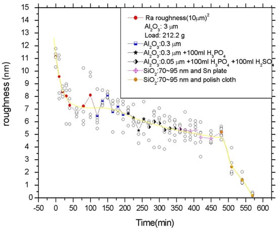
Figure 1.
Surface roughness of polished sapphire as a function of polishing time using γ-Al2O3 and SiO2 slurry. Five data points were taken via AFM at each polishing time. Only the center data are colored with symbols to indicate the different polishing methods used. The smooth yellow curve is included to guide the eye.
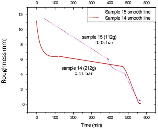
Figure 2.
The general trend in the reduction in surface roughness via applying pressure with loading values of 112 g (0.05 bar) and 212 g (0.11 bar). Data are smoothened.
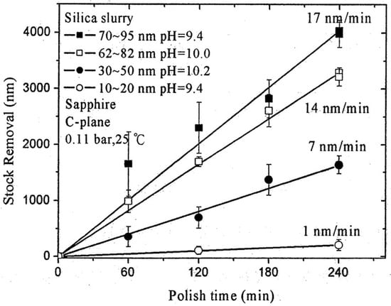
Figure 3.
The removal rate of sapphire with SiO2 slurry at different colloidal particle sizes.
3.2. Surface Characterization
For successful epitaxial growth, the top surface of the substrate must be smooth, clean, and free from atomic disorder. Figure 4 shows a typical AFM image of colloidal SiO2 polishing. As polishing time increases, the roughness (Ra) value decreases. However, the Ra value eventually stabilizes at around 0.1–0.3 nm. Figure 4a,b show examples of AFM surface morphology with Ra values of 0.481 nm and 0.158 nm, respectively. The scanning area is 10 μm × 10 μm. For the sample with Ra = 0.158 nm, the surface is featureless and smooth. Figure 4c,d plot three-line scan profiles, with each line separated by 2.5 μm in the y-direction. From Figure 4d, flat terraces of 1–2 μm wide can be identified on a smooth surface. Figure 5 shows the EDS measurement of the surface, revealing the presence of only Al, O, and C elements. The atomic percentages are Al:O:C = 28:65:6, indicating the presence of an organic thin film on the surface. This organic contamination can easily be removed by solvents and then by heating the sample at 130 °C in a vacuum of 10−8 Torr. No LEED pattern was observed before heating the sample in a high vacuum. Afterwards, a clear hexagonal LEED diffraction pattern was observed (see Figure 6). The LEED intensity remains similar after heat treatment at higher temperatures up to 300 °C, indicating that most of the organic contamination has been removed. This result also demonstrates that the top one to two monolayers of atoms are arranged in well-ordered hexagonal symmetry, indicating that the wafer is ready for the next epitaxial process. Additionally, AES was used to verify the surface contamination, particularly the carbon contamination, as AES is more sensitive in determining the concentration of low-Z elements.
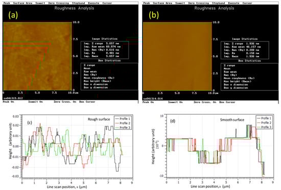
Figure 4.
AFM surface morphology: (a) Ra = 0.481 nm; (b) Ra = 0.158 nm. (c) Three-line scan profiles on the rough surface (a,d) three-line scan profiles on the smooth surface (b). The three lines are separated by 2.5 μm in the y-direction. The vertical range of (c) is three times larger compared to that of (d). As shown in (b), the surface is featureless when Ra = 0.158 nm, indicating that a smooth surface was prepared.
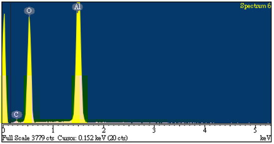
Figure 5.
EDS measurement of the sapphire surface after CMP. Al and O are found, and C contamination is also detected.
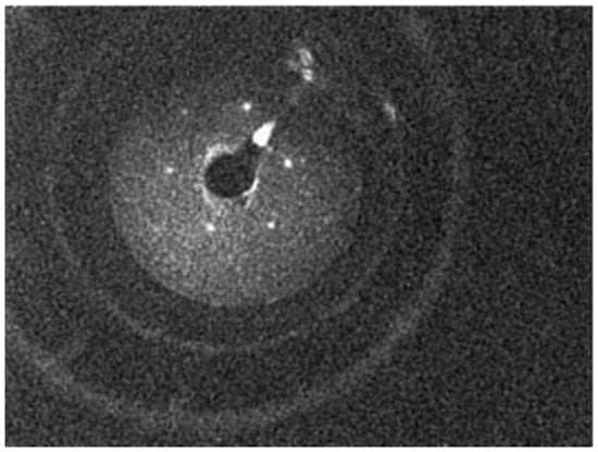
Figure 6.
The hexagonal LEED pattern with an electron energy of 120 eV on the super-polished sapphire surface Al2O3 (0001) after heating at 130 °C. Before the heating treatment, no electron diffraction peaks were found.
XRR measurements were also performed on polished Al2O3 (0001). The results showed that the root-mean-square roughness of the sapphire surface is around 0.2 nm, which is consistent with the AFM data (0.16 nm). XRR measurements provide more reliable statistical values than AFM data, which is limited to a narrow scanning area and is dependent on tip shape [11,12]. For the XRR data analysis, the Gen-X program, developed by Glavic and Björck [15], was used to fit the experimental results. Figure 7 shows the measurement of sample 14 on the as-polished sample without removing the surface contamination. Although sample 14 exhibited lower surface roughness at a pressure of 0.11 bar during the polishing stage, an organic thin film of about 1.2 nm was found on the surface via XRR measurement. Sample 15, polished at a lower pressure of 0.05 bar, exhibited significantly less contamination than the higher-pressure sample. In-plane sapphire diffraction peaks were also observed by GIXD. The six-fold symmetry of the in-plane diffraction peaks was identified by an azimuthal scan (Phi scan). The width of the rocking curves of the in-plane diffraction peaks, such as the (11–20) and (1–100) peaks, is 0.02°, which is limited by the divergence of the incident beam of the B17 beamline at the NSRRC. The FWHM of the radial scan of the in-plane peaks is also limited by the instrument resolution, indicating that the coherence length of the sapphire surface in the plane is larger than one micrometer.
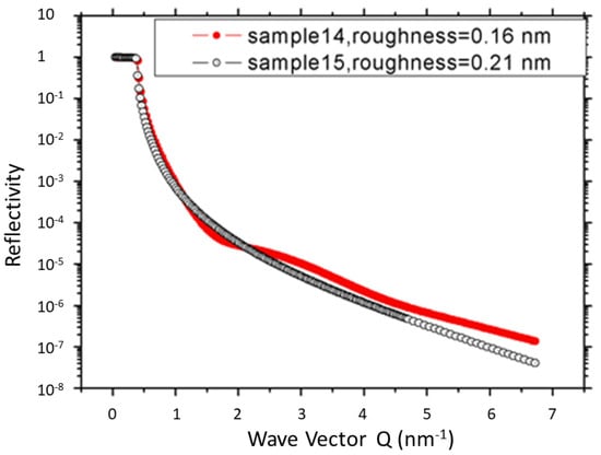
Figure 7.
The typical X-ray reflectivity measurement of the super-polished sapphire surface Al2O3 (0001). The wave vector Q = 4πsinθ/λ, where θ is the incidence angle and λ is the wavelength of the X-ray, which is 0.154 nm.
3.3. Epitaxial Thin Film Test
To ascertain whether the polished sapphire surface was adequately prepared for epitaxial growth, we examined the epitaxy of GaN deposited on an Al2O3 (0001) surface. We used a four-circle X-ray diffractometer to characterize the epitaxial growth of the thin film. GaN epitaxial layers were grown by metal–organic chemical vapor deposition (MOCVD) in a horizontal flow reactor [16,17]. The main reactant sources were separated by a quartz plate. TMGa (trimethylgallium), with H2 as the carrier gas, flowed into the upper stream, and NH3, with a small amount of H2, was introduced into the bottom stream. The substrate temperature was cooled to 525 °C to grow a 25 nm nucleation layer and was then raised to 1000 °C to grow the 1 µm thick GaN epitaxial layer.
To understand the growth mode of the thin film, the surface energy of sapphire and GaN is investigated. The surface energies of sapphire (c-plane) have been reported to be around 1.65–1.98 J/m2 [18] and 3.36 J/m2 [19], whereas those of GaN (0001) have been reported to be 1.6–3.2 J/m2 [20] and 5.7–5.9 J/m2 [21]. Surface energy depends on surface termination, reconstruction, surface polishing, annealing conditions, and environmental exposure. Nevertheless, the typical growth mode is the Stranski–Krastanov (S-K) mode, which is a hybrid of layer-by-layer growth at the beginning and island growth thereafter. This may be due to the similar surface energies of the c-planes of the GaN and sapphire substrates.
The crystallographic orientation of the sample is GaN [0001]//Al2O3 [0001] and GaN [11–20]//Al2O3 [1–100]. This orientation was determined using an azimuthal scan (also known as a Phi scan) on a standard four-circle diffractometer, as illustrated in Figure 8. The orientation relationship between the epitaxial film and the substrate was measured using hk-circle scans. An hk-circle scan is similar to a pole figure scan in X-ray diffraction. Figure 8a shows the geometry of the azimuthal scan (or hk-circle scan) about the normal plane axis. Figure 8b shows an hk-circle scan rotating about the GaN (0001) axis while scanning across the GaN {1–103} family. Six diffraction peaks can be found. The hk-circle scan of the Al2O3 {1–104} family peaks about the Al2O3 (0001) axis shows threefold symmetry (see Figure 8c). The sharp Bragg diffraction peaks reveal that the GaN thin film was successfully epitaxial grown on the Al2O3 (0001) substrate. The absence of extra peaks indicates that the GaN epitaxial film is a single-domain crystalline.
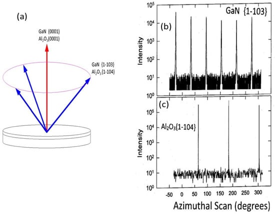
Figure 8.
(a) The geometry of the hk-circle scan (or azimuthal scan) around the plane normal axis of GaN (0001) and Al2O3 (0001) axes. (b) The azimuthal scan of GaN {1–103}. (c) The azimuthal scan of Al2O3 {1–104}.
Further evidence of the high quality of the epitaxy at the GaN/sapphire interface can be seen in the rocking curve measurements of the GaN (0002) diffraction peak (see Figure 9). The GaN (0002) rocking curve consists of two components. The sharp peak component has a narrow width of 0.025°, which matches that of the in-plane sapphire substrate rocking curve. This suggests that a few GaN atomic layers were grown in parallel along the flat sapphire atomic plane. The second component of the GaN (0002) rocking curve has a broad FWHM of around 0.5°, indicating a large mosaic spread of the GaN thin film. Presumably, the broad component originates from the upper GaN layer due to the formation of misfit dislocations. Misfit dislocations can only form once misfit strain has accumulated beyond a critical thickness. The sharp component presumably occurs near the sapphire interface, where misfit strain develops without misfit dislocation distortion. Consequently, the rocking curve is as sharp as the rocking curve of the surface sapphire diffraction peaks. This result also partly supports the idea that a super-polished sapphire surface is capable of epitaxially growing a flat GaN thin film near the interface. Long-range rotational displacement gives rise to sharp and broadened diffuse peaks in the rocking curve of the Bragg peak. This phenomenon has also been observed in the works of Miceli et al. [22,23] regarding the ErAs (001)/GaAs (001) and In0.7As0.3P (001)/GaAs (001) systems. Their systems exhibit the coexistence of a sharp peak (resolution-limited linewidth), and diffuse scattering in the rocking curve occurs; the former arises from long-range order, and the latter comes from short-range correlations. As can be seen in Figure 9, our GaN (0002) rocking curve also consists of two components: one is sharp (limited by instrument resolution), and the other is broad and diffuse. This result may be correlated with the S-K growth mode. In layer-by-layer growth, the first few layers that grow align well with the smooth substrate. Once the GaN thickness exceeds the critical thickness at which misfit dislocations take place, island growth occurs. The high density of dislocations results in the diffuse component of the rocking curve.
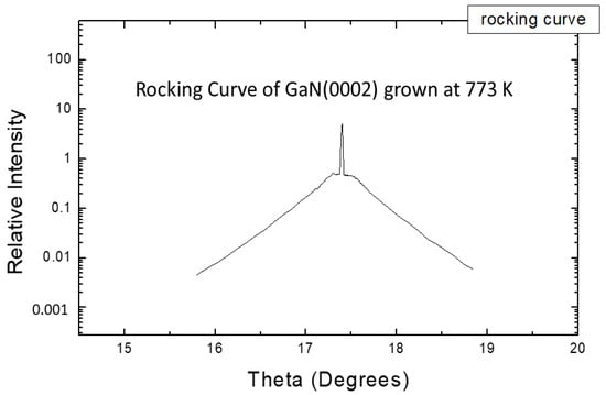
Figure 9.
The rocking curve of GaN (0002) diffraction peaks exhibited both a sharp and a broad diffuse component.
4. Conclusions
The super-polishing procedure of a sapphire (Al2O3, 0001) wafer was demonstrated: first, γ-Al2O3 was used, followed by colloidal SiO2 particles. The surface morphology was characterized using AFM, EDS, AES, XRR, LEED, and GIXD. In particular, the bright LEED pattern is sensitive to the structure of the top layer of the sapphire surface. A single-crystal surface was identified. It is possible to prepare a single-domain epitaxy film of GaN (0002) on Al2O3 (0001). Additionally, the rocking curve of the GaN (0002) Bragg peak in the GaN (0001)/Al2O3 (0001) system has two components: one very sharp peak and a broad diffuse peak. This demonstrates the interface between the sapphire and GaN film with long-range order. These results show that the substrate is ready for further MBE and CVD epitaxial applications.
Author Contributions
Conceptualization, C.-H.L. (Chih-Hao Lee); methodology, C.-H.L. (Chih-Hao Lee); software, C.-H.L. (Chih-Hao Lee); formal analysis, C.-H.L. (Chih-Hong Lee); investigation, C.-H.L. (Chih-Hao Lee); resources, C.-H.L. (Chih-Hao Lee); data curation, C.-H.L. (Chih-Hong Lee); writing—original draft preparation, C.-H.L. (Chih-Hong Lee); writing—review and editing, C.-H.L. (Chih-Hao Lee); supervision, C.-H.L. (Chih-Hao Lee). All authors have read and agreed to the published version of the manuscript.
Funding
This project is partly supported by the National Science and Technology Council, Taiwan, under the contract of NSC91-2622-E007-024-CC3.
Data Availability Statement
The data are available upon request to the corresponding author.
Acknowledgments
The synchrotron radiation beamline offered by NSRRC is acknowledged. We are grateful to the Hantek Company for providing the sapphire wafer and chemical reagents.
Conflicts of Interest
The authors declare no conflicts of interest.
References
- Bennett, J.M.; Shaffer, J.J.; Shibano, Y.; Namba, Y. Float polishing of optical materials. Appl. Opt. 1987, 26, 696–703. [Google Scholar] [CrossRef]
- Hader, B.; Weis, O. Superpolishing sapphire: A method to produce atomically flat and damage free surfaces. Surf. Sci. 1989, 220, 118–130. [Google Scholar] [CrossRef]
- Weis, O. Direct contact superpolishing of sapphire. Appl. Opt. 1992, 31, 4355–4362. [Google Scholar] [CrossRef]
- Gutsche, H.W.; Moody, J.W. Polishing of Sapphire with Colloidal Silica. J. Electrchem. Soc. 1978, 125, 136–138. [Google Scholar] [CrossRef]
- Li, Z.; Deng, Z.; Ge, J.; Liu, T.; Wan, L. Experimental and theoretical analysis of single-sided and double-sided chemical mechanical polishing of sapphire wafers. Int. J. Adv. Manuf. Technol. 2022, 119, 5095–5106. [Google Scholar] [CrossRef]
- Zhang, Z.; Liu, J.; Hu, W.; Zhang, L.; Xie, W.; Liao, L. Chemical mechanical polishing for sapphire wafers using a developed slurry. J. Manuf. Process 2021, 62, 762–770. [Google Scholar] [CrossRef]
- Zhang, Z.; Liu, W.; Song, Z.; Hu, X. Two-step chemical mechanical polishing of sapphire substrates. J. Electrochem. Soc. 2020, 157, H688–H691. [Google Scholar] [CrossRef]
- Xie, W.; Zhang, Z.; Liao, L.; Liu, J.; Su, H.; Wang, S.; Guo, D. Green chemical mechanical polishing of sapphire wafers using a novel slurry. Nanoscale 2020, 12, 22518–22526. [Google Scholar] [CrossRef] [PubMed]
- Xu, W.; Cheng, Y.; Zhong, M. Effects of process parameters on chemical-mechanical interactions during sapphire polishing. Microelectron. Eng. 2019, 216, 111029. [Google Scholar] [CrossRef]
- Li, S.; Fu, J.; He, Z.; Luo, Y.; Wu, S. Nanomaterials and Equipment for Chemical–Mechanical Polishing of Single-Crystal Sapphire Wafers. Coatings 2023, 13, 2081. [Google Scholar] [CrossRef]
- Lee, C.H.; Pen, W.Y.; Lin, M.Z.; Yu, K.L.; Hsueh, J.C. A comparison between the atomic force microscopy and X-ray reflec tivity on the characterization of surface roughness. Inter. J. Nano-Sci. 2023, 2, 343–348. [Google Scholar] [CrossRef]
- Su, H.C.; Lee, C.H.; Lin, M.Z.; Huang, T.Z. A comparison between X-ray reflectivity and atomic force microscopy on the characterization of a surface roughness. Chin. J. Phys. 2012, 50, 291–300. [Google Scholar]
- Tsang, K.L.; Lee, C.H.; Jean, Y.C.; Dann, T.E.; Chen, J.R.; D’Amico, K.L.; Oversluizen, T. The Wiggler X-ray Beamlines at SRRC. Rev. Sci. Instrum. 1995, 66, 1812–1814. [Google Scholar] [CrossRef]
- Certified Scientific Software. Spec Manual: X-Ray Diffraction Software, Version 3; Certified Scientific Software: Cambridge, MA, USA, 2017. [Google Scholar]
- Glavic, A.; Björck, M. Gen-X reflectivity program. J. Appl. Crystallogr. 2022, 55, 1063. [Google Scholar] [CrossRef] [PubMed]
- Nakamura, S.; Harada, Y.; Seno, M. Novel metalorganic chemical vapor deposition system for GaN growth. Appl. Phys. Lett. 1991, 58, 2021–2023. [Google Scholar] [CrossRef]
- Yang, C.C.; Koh, P.L.; Wu, M.C.; Lee, C.H.; Chi, G.C. Effects of H2/NH3 Flow-Rate Ratio on the luminescent, structural, and electrical properties of GaN epitaxial layers grown by MOCVD. J. Electron. Mater. 1999, 28, 1096–1100. [Google Scholar] [CrossRef]
- Kurita, T.; Uchida, K.; Oshiyama, A. Atomic and electronic structures of α-Al2O3 surfaces. Phys. Rev. B 2010, 82, 155319. [Google Scholar] [CrossRef]
- Bakholdin, S.I.; Maslov, V.N. Simulation of surface energies of sapphire crystals. Phys. Solid State 2015, 57, 1236–1243. [Google Scholar] [CrossRef]
- Razia; Chugh, M.; Ranganathan, M. Surface energy and surface stress of polar GaN (0001). Appl. Surf. Sci. 2021, 566, 150627. [Google Scholar] [CrossRef]
- Dreyer, C.E.; Janotti, A.; Van de Walle, C.G. Absolute surface energies of polar and nonpolar planes of GaN. Phys. Rev. B 2014, 89, 081005(R). [Google Scholar] [CrossRef]
- Miceli, P.F.; Palmstrgm, C.J. X-ray scattering from rotational disorder in epitaxial films: An unconventional mosaic crystal. Phys. Rev. 1995, 51, 5506–5509. [Google Scholar] [CrossRef] [PubMed]
- Miceli, P.F.; Weatherwax, J.; Krentse, T.; Palmstrom, C.J. Specular and diffuse reflectivity from thin films containing misfit dislocations. Phys. B 1996, 221, 230–234. [Google Scholar] [CrossRef]
Disclaimer/Publisher’s Note: The statements, opinions and data contained in all publications are solely those of the individual author(s) and contributor(s) and not of MDPI and/or the editor(s). MDPI and/or the editor(s) disclaim responsibility for any injury to people or property resulting from any ideas, methods, instructions or products referred to in the content. |
© 2025 by the authors. Licensee MDPI, Basel, Switzerland. This article is an open access article distributed under the terms and conditions of the Creative Commons Attribution (CC BY) license (https://creativecommons.org/licenses/by/4.0/).