Abstract
Intermediate-band photovoltaics promise single-junction efficiencies that exceed the Shockley and Queisser limit, yet viable material platforms and device geometries remain under debate. Here, we perform comprehensive two-dimensional device-scale simulations using Silvaco Atlas TCAD to analyze p-i-n In0.20Ga0.80N solar cells in which the intermediate band is supplied by In0.35Ga0.65N quantum dots located inside the intrinsic layer. Quantum-dot diameters from 1 nm to 10 nm and areal densities up to 116 dots per period are evaluated under AM 1.5G, one-sun illumination at 300 K. The baseline pn junction achieves a simulated power-conversion efficiency of 33.9%. The incorporation of a single 1 nm quantum-dot layer dramatically increases efficiency to 48.1%, driven by a 35% enhancement in short-circuit current density while maintaining open-circuit voltage stability. Further increases in dot density continue to boost current but with diminishing benefit; the highest efficiency recorded, 49.4% at 116 dots, is only 1.4 percentage points above the 40-dot configuration. The improvements originate from two-step sub-band-gap absorption mediated by the quantum dots and from enhanced carrier collection in a widened depletion region. These results define a practical design window centred on approximately 1 nm dots and about 40 dots per period, balancing substantial efficiency gains with manageable structural complexity and providing concrete targets for epitaxial implementation.
1. Introduction
Group-III-nitride semiconductors, particularly the InxGa1−xN alloy system, exhibit a direct band gap that can be continuously tuned from approximately 0.7 to 3.4 eV, large absorption coefficients, high carrier mobilities and excellent radiation hardness, attributes that position them at the forefront of research on next-generation single-junction photovoltaics [,]. Even with these advantages, any device built on a single absorptive transition remains confined by the Shockley and Queisser limit, because photons with energies below the band gap are not absorbed while carriers generated well above the gap lose excess energy to thermalisation [,]. The intermediate-bandgap solar cell (IBSC) concept (see Figure 1), first articulated by Luque and Martí [,], addresses this loss channel by placing a partially filled miniband—hereafter the intermediate band (IB)—inside the forbidden gap so that two low-energy photons can be absorbed sequentially, raising the detailed-balance ceiling to ≈63% under concentration and 47% at one sun. Quantum dots provide an experimentally accessible route for realising the intermediate band because discrete states that arise from three-dimensional confinement can couple into minibands when dots are vertically stacked; their energies can be adjusted through composition, size and strain, and they integrate naturally within standard epitaxial workflows [,]. Prototype InAs/GaAs and InGaAs/GaAs devices have already demonstrated extended spectral response and enhanced short-circuit current, yet reported power-conversion efficiencies trail theoretical expectations, a shortfall traced to incomplete optimization of dot diameter, areal density, strain management and polarization fields [,]. This is particularly advantageous compared to the more traditional InAs/GaAs system, where a large lattice mismatch (~7%) often leads to defect formation and limits the ability to independently optimize dot morphology and strain [,,]. The InGaN system, in contrast, allows for tunable strain by adjusting the indium content of both the dot and the barrier, providing a more robust platform for realizing the high-quality heterostructures required for high-efficiency devices [,,]. Within the III-nitride family, the case for quantum-dot intermediate-band photovoltaics is particularly compelling: an In-rich InGaN dot lattice embedded in a wider-gap InGaN matrix aligns intermediate levels favourably with the solar spectrum, and wurtzite polarization fields can assist carrier extraction if adequately controlled [,]. Recent numerical studies predict that careful co-optimization of dot size, areal density and hydrostatic pressure can push the efficiency of III-nitride intermediate-band devices well beyond current benchmarks [,], yet exhaustive experimental mapping of this multidimensional design space is impractical, which makes advanced technology computer-aided design essential [,].
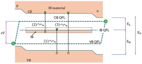
Figure 1.
Band diagram of a p-i-n (p-type/intrinsic/n-type) solar cell with an intermediate band (IB) located within the bandgap (EG) of the host material. The IB enables a two-step photon absorption process to generate an electron–hole pair from two sub-bandgap photons. Transition (1) represents the excitation of an electron from the valence band (VB) to the IB. Transition (2) shows the subsequent excitation of that electron from the IB to the conduction band (CB). Together, these two transitions are equivalent to the single-photon absorption across the full bandgap shown in transition (3). This mechanism allows the cell to utilize photons with energies less than EG, increasing the short-circuit current while ideally preserving the output voltage, which is determined by the separation of the quasi-Fermi levels (QFLs) of the CB and VB.
While TCAD has been successfully applied to optimize the doping and thickness of conventional InGaN single-junction cells [], the present investigation closes a critical gap by systematically charting the combined influence of quantum-dot diameter and areal density on every major photovoltaic figure of merit within a manufacturable p-i-n InGaN architecture. Two-dimensional Silvaco Atlas simulations incorporating effective-mass quantum-correction potentials, composition-dependent polarization charges and experimentally validated recombination pathways are applied to an In0.20Ga0.80N matrix containing In0.35Ga0.65N quantum dots whose diameters range from one to ten nanometres and whose population spans zero to one hundred sixteen per device period [,]. The resulting efficiency landscape peaks at forty-eight percent when dots measure roughly one nanometre and number about forty per period, a value that approaches the unconcentrated theoretical limit while remaining compatible with contemporary metal-organic vapour-phase epitaxy. These quantitative guidelines establish a realistic target for experimental efforts and demonstrate that judiciously engineered InGaN quantum-dot intermediate bands can transcend the traditional efficiency ceiling of single-junction photovoltaics [,].
2. Materials and Methods
2.1. InGaN-Based Solar Cell Structure
Two-dimensional drift-diffusion simulations were executed utilizing the Atlas module of Silvaco TCAD software (version 4.6.1.R) to investigate an In0.20Ga0.80N p-i-n solar cell architecture incorporating an intrinsic layer containing a planar array of In0.35Ga0.65N quantum dots (Figure 2). The selection of In0.35Ga0.65N for the quantum dots and In0.20Ga0.80N for the host matrix was based on bandgap engineering principles aimed at optimizing spectral absorption. This combination creates a host bandgap of approximately 2.66 eV and a confinement potential suitable for forming an intermediate band located at an energy level that facilitates two-step absorption of high-flux regions of the AM 1.5G solar spectrum. The quantum dot structures were modelled as square prismatic geometries with lateral edge dimensions (designated as quantum dot width, L) where L = LX = LY, and vertical height parameters systematically varied across a range of 1 nm to 10 nm to enable comprehensive parametric optimization. Quantum dot areal density per period was methodically swept from 0 to 116 structures per unit area, facilitating detailed analysis of density-dependent photovoltaic performance characteristics, as documented in the Results section. A control device consisting of a dot-free In0.20Ga0.80N homojunction was simulated in parallel configuration to establish baseline reference parameters for comparative analysis. All computational modelling assumed standard testing conditions including AM 1.5G solar spectrum, one-sun illumination intensity (100 mW·cm−2) at 300 K operating temperature, with the built-in Atlas optical-generation model employed for accurate photogeneration calculations throughout the device architecture.
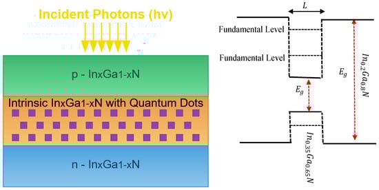
Figure 2.
Schematic of the simulated InxGa1−xN p-i-n solar cell structure. The device consists of p-type and n-type In0.20Ga0.80N layers surrounding an intrinsic (i) In0.20Ga0.80N region. Within this intrinsic layer, a planar array of In0.35Ga0.65N quantum dots (QDs) is embedded to form the intermediate band. Incident photons (hv) generate electron–hole pairs, with the QDs enabling the absorption of sub-bandgap photons. The second panel in this figure illustrates the schematic 1D-band diagram of the QD structure based on In0.35Ga0.65N/In0.20Ga0.80N materials showing the energy levels for the corresponding Qd’s dimension ().
Table 1 displays the obtained results for the energy levels of QD-based In0.35Ga0.65N/In0.20Ga0.80N for different values of the QD dimension. Notice that the energy levels which are not mentioned correspond to the unbound states, i.e., their energy level are greater than the confinement potential barrier which is proportional to the difference between the band gap energies of well and barrier materials. For instance, it is clear that with increasing QD size, both energies decrease.

Table 1.
The energy level (meV) of QD-based In0.35Ga0.65N/In0.20Ga0.80N of the fundamental and first exited states.
2.2. Material Parameters and Physical Models
The composition-dependent material constants that determine carrier generation, transport and recombination in the InxGa1−xN system were implemented through analytical bowing laws and experimentally benchmarked coefficients. The ternary band gap was described by []:
with = 0.78 eV, = 3.42 eV and a bowing parameter b = 1.43 [,]. The corresponding electron affinity followed []:
while the relative permittivity was taken as []:
It is important to note that while our model includes the macroscopic effects of strain through built-in polarization charges and utilizes standard models for non-radiative recombination, a detailed microscopic analysis of defect formation due to lattice mismatch remains a topic for future investigation.
2.3. Electrical Parameters
Photovoltaic figures of merit were extracted from each simulated J–V curve using the standard definitions adopted in the III-nitride device literature. The power-conversion efficiency (PCE) is the ratio of the maximum electrical power delivered by the cell to the incident optical power . Because occurs at the operating point (, ), PCE can also be expressed through the open-circuit voltage , the short-circuit current density and the fill factor FF:
The fill factor is defined as the ratio of the maximum electrical power to the ideal rectangular power , :
In all simulations, was fixed at 100 mWcm−2, corresponding to one-sun AM 1.5G illumination at 300 K; for completeness, the incident solar power density can be expressed in SI units as with the Stefan–Boltzman constant .
3. Results and Discussion
This section presents a comprehensive simulation analysis of Indium Gallium Nitride (InGaN)-based quantum dot intermediate-band solar cells (QD-IBSCs) under standard AM1.5 illumination. The investigation systematically explores the influence of two critical design parameters: the physical dimensions of the quantum dots (QDs) and the number of stacked QD layers within the intrinsic (i) region of a p-i-n solar cell structure. The analysis aims to elucidate the mechanisms driving performance enhancements and identify optimal configurations for maximizing power conversion efficiency.
3.1. The Influence of Quantum Dot Dimensions on Solar Cell Performance
The performance of a QD-IBSC is intrinsically linked to the quantum confinement effects dictated by the size of the QDs. To investigate this relationship, the lateral dimensions (L) of the In0.35Ga0.65N QDs were varied, and the corresponding current density–voltage (J–V) characteristics were simulated, as shown in Figure 3a.
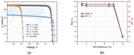
Figure 3.
Quantum dot size-dependent photovoltaic performance characteristics of p-i-n solar cells; (a) Current density–voltage (J–V) characteristics demonstrating the influence of quantum dot diameter (L = 1–10 nm) on device electrical behaviour under standard illumination conditions. The reference curve represents conventional devices without quantum dot integration; (b) Power conversion efficiency (PCE) and fill factor (FF) optimization as a function of quantum dot dimensions, illustrating the critical size threshold for QDIBSC solar cell performance enhancement.
Figure 3a displays illuminated J–V curves for devices that contain one In0.35Ga0.65N QD plane whose lateral dimension L is swept from 1 to 10 nm. A critical size-dependent threshold for solar cell performance is revealed. The photovoltaic metrics remain high for dot diameters (L) up to 8 nm but collapse for larger sizes. When L ≤ 2 nm the short-circuit current density rises to JSC = 45 mA/cm2 while the open-circuit voltage is retained at VOC = 1.19 V; both metrics eclipse the dot-free homojunction. This confirms that an intermediate band capable of two-photon absorption can be formed without compromising the quasi-Fermi-level splitting, in agreement with the voltage-preservation principle of Luque and Martí [,]. In contrast, dots larger than 8 nm collapse the J–V curve, VOC plunges below 0.5 V because weak confinement merges the discrete IB states into a continuum and introduces mid-gap traps that accelerate non-radiative recombination.
This trend is quantified in Figure 3b, which plots the power conversion efficiency (PCE) and fill factor (FF) as a function of QD size. The highest performance is achieved with 1 nm QDs, yielding a PCE of approximately 47.5% and an FF of 88.5%. A sharp decline in both metrics is evident for QD dimensions greater than 8 nm, with the PCE falling below 15% for 10 nm QDs. These results underscore that strong 3D quantum confinement, achieved with QD dimensions on the order of 1–2 nm, is essential for creating an effective intermediate band and maximizing device efficiency.
3.2. Optimizing the Number of the Incorporated QDs
To establish the fundamental benefit of the QD-IBSC architecture, we first compare a standard InGaN p-i-n solar cell (without QDs) to a device incorporating a single layer of 12 QDs. Figure 4a presents the J–V characteristics of both cells. The introduction of QDs results in a substantial increase in short-circuit current density, from JSC ≈ 33.7 mA/cm2 for the baseline cell to JSC ≈ 40.9 mA/cm2 for the 12-QD cell. This 21% increase in current is the primary signature of a functioning intermediate band, which enables the absorption of sub-bandgap photons to generate additional electron–hole pairs. This enhancement comes at the cost of a slight reduction in open-circuit voltage, from VOC ≈ 1.24 V to 1.23 V, a common trade-off in QD-IBSCs often linked to increased recombination through QD states.
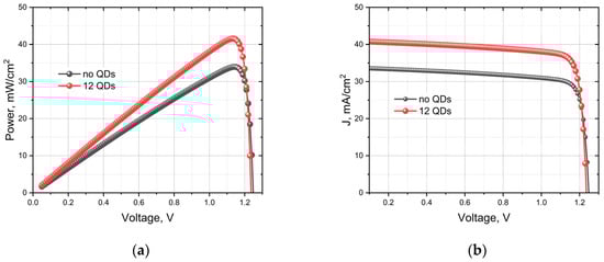
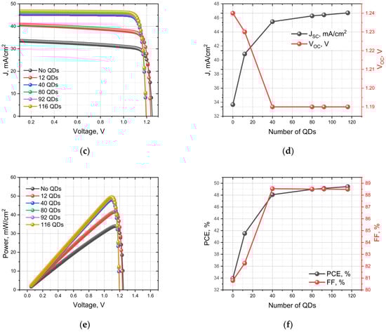
Figure 4.
Comprehensive electrical characterization and quantum dot optimization in QD-IBSC devices; (a) Power–voltage characteristics comparing baseline (no QDs) and 12 QD-enhanced p-i-n junction architectures, demonstrating enhanced power output through quantum dot integration; (b) Current density–voltage characteristics showing improved JSC with QD incorporation while maintaining stable VOC; (c) Systematic J–V performance enhancement across QD concentrations (0–116 QDs) under AM 1.5G illumination, revealing progressive current density improvements; (d) Short-circuit current density and open-circuit voltage dependencies on QD number, showing JSC saturation beyond 40 QDs with stable VOC ≈ 1.19 V; (e) Power–voltage optimization across all QD concentrations, demonstrating maximum power output at 116 QDs; (f) Power conversion efficiency and fill factor evolution, achieving optimal PCE plateau (≈49%) at 40–116 QD concentrations with FF stabilization at 88%.
The net effect on power output is illustrated in the power–voltage (P–V) curves in Figure 4b. The enhanced current generation in the 12-QD device leads to a significant boost in maximum power density (Pmax) to approximately 41.5 mW/cm2, compared to ~34 mW/cm2 for the cell without QDs. This confirms that the inclusion of QDs provides a clear pathway to higher overall efficiency [].
Building upon the established benefit of QD incorporation, we next investigated the effect of increasing the number of QD layers within the intrinsic region. Figure 4c,d show the J–V and P–V characteristics, respectively, for devices containing 0, 12, 40, 80, 92, and 116 QDs.
As seen in Figure 4c, increasing the number of QDs systematically increases the short-circuit current density. This is expected, as more QDs provide a greater volume for sub-bandgap photon absorption. However, the incremental gain in Jsc diminishes as more layers are added, suggesting a saturation effect. This saturation is a direct consequence of the Beer–Lambert law; once the initial QD layers have absorbed most of the available sub-bandgap photons, subsequent layers contribute progressively less to current generation.
This saturation behaviour is more clearly summarized in Figure 4e,f. Figure 4e plots the evolution of JSC and VOC with the number of QDs. JSC rises sharply from 33.7 mA/cm2 (0 QDs) to 45.6 mA/cm2 (40 QDs), after which it increases much more slowly to 46.5 mA/cm2 (116 QDs). Meanwhile, after the initial drop, the VOC remains relatively stable at approximately 1.19 V for all QD-containing configurations.
The ultimate determinant of performance, the PCE, is shown in Figure 4f. The efficiency dramatically improves from 33.9% for the baseline cell to 48.1% for the cell with 40 QD layers. Beyond this point, the efficiency plateaus, reaching only 48.9% with 116 QDs. This demonstrates that there is an optimal number of QD layers, beyond which the marginal gains in JSC do not translate into a meaningful increase in overall efficiency. The fill factor (FF) follows a similar trend, increasing significantly up to 40 QDs and then saturating at a high value of ~88.5%.
4. Conclusions
This comprehensive two-dimensional TCAD modelling demonstrates that strategically incorporating In0.35Ga0.65N quantum dots into the intrinsic region of a p-i-n In0.2Ga0.8N solar cell creates an effective intermediate band, enabling two-step sub-bandgap absorption and significantly expanding the depletion region.
The optimized device configuration achieves a remarkable simulated power-conversion efficiency of 48.1%, representing a 41% relative improvement over the baseline 33.9% pn structure. This enhancement is primarily attributed to a 35% increase in short-circuit current density while maintaining open-circuit voltage stability—a key requirement for intermediate-band solar cell operation.
The analysis reveals diminishing returns beyond approximately 40 quantum dots per period, establishing a practical design window that balances performance enhancement with fabrication complexity. These quantitative guidelines provide clear targets for experimental implementation:
- Optimal quantum dot size: ~1 nm diameter;
- Optimal quantum dot density: ~40 dots per period;
- Expected efficiency improvement: >40% relative to conventional pn junctions.
These results demonstrate the significant potential for InGaN quantum-dot intermediate-band solar cells to surpass traditional single-junction efficiency limits while remaining compatible with existing epitaxial growth technologies.
Author Contributions
Conceptualization, writing—original draft preparation, and investigation, S.A., H.E.G. and W.B.; methodology, S.A., formal analysis, S.A., H.E.G. and W.B.; data curation, writing—review and editing, and supervision, H.E.G. and W.B. All authors have read and agreed to the published version of the manuscript.
Funding
This research received no external funding.
Data Availability Statement
The original contributions presented in the study are included in the article material, further inquiries can be directed to the corresponding authors.
Conflicts of Interest
The authors declare no conflicts of interest.
Abbreviations
The following abbreviations are used in this manuscript:
| AM 1.5G | Air Mass 1.5 Global (standard solar spectrum) |
| FF | Fill Factor |
| IB | Intermediate Band |
| IBSC | Intermediate-Band Solar Cell |
| PCE | Power Conversion Efficiency |
| TCAD | Technology Computer-Aided Design |
| QD | Quantum Dot |
| QD-IBSC | Quantum Dot Intermediate Band Solar Cell |
| J–V | Current Density–Voltage |
| P–V | Power–Voltage |
| JSC | Short-Circuit Current Density |
| VOC | Open-Circuit Voltage |
References
- Mesrane, A.; Rahmoune, F.; Mahrane, A.; Oulebsir, A. Design and Simulation of InGaN p-n Junction Solar Cell. Int. J. Photoenergy 2015, 2015, 594858. [Google Scholar] [CrossRef]
- Vilbois, L.; Cheknane, A.; Bensaoula, A.; Boney, C.; Benouaz, T. Simulation of a solar cell based on InGaN. Energy Procedia 2012, 18, 795–806. [Google Scholar] [CrossRef]
- Fabien, C.A.; Doolittle, W.A. Guidelines and limitations for the design of high-efficiency InGaN single-junction solar cells. Sol. Energy Mater. Sol. Cells 2014, 130, 354–363. [Google Scholar] [CrossRef]
- Fang, Y. Simulation of High Temperature InGaN Photovoltaic Devices; Arizona State University: Tempe, AZ, USA, 2017. [Google Scholar]
- Luque, A.; Martí, A. Increasing the efficiency of ideal solar cells by photon induced transitions at intermediate levels. Phys. Rev. Lett. 1997, 78, 5014. [Google Scholar] [CrossRef]
- Luque, A.; Martí, A.; Stanley, C. Understanding intermediate-band solar cells. Nat. Photonics 2012, 6, 146–152. [Google Scholar] [CrossRef]
- Martí, A.; López, N.; Antolin, E.; Cánovas, E.; Stanley, C.; Farmer, C.; Cuadra, L.; Luque, A. Novel semiconductor solar cell structures: The quantum dot intermediate band solar cell. Thin Solid Film. 2006, 511, 638–644. [Google Scholar] [CrossRef]
- Jenks, S.; Gilmore, R. Material selection for the quantum dot intermediate band solar cell. In Quantum Dot Solar Cells; Springer: Berlin/Heidelberg, Germany, 2013; pp. 135–166. [Google Scholar]
- Amin, S.A.; Hasan, M.T.; Islam, M.S. The effects of interdot spacing and dot size on the performance of InGaAs/GaAs QDIBSC. Int. J. Photoenergy 2017, 2017, 9160381. [Google Scholar] [CrossRef]
- Chettri, D.; Singh, T.J.; Singh, K.J. InAs/GaAs quantum dot solar cell. Int. J. Electron. Electr. Comput. Syst. 2017, 6, 221–224. [Google Scholar]
- Li, M.; Duan, J.; Jin, Z.; Pan, S.; Zhan, W.; Chen, J.; Yu, J.; Cheng, X.; Ni, Z.; Jin, C. Enhanced Radiation Hardness of InAs/GaAs Quantum Dot Lasers for Space Communication. Laser Photonics Rev. 2025, 19, 2500148. [Google Scholar] [CrossRef]
- Mano, T.; Ohtake, A.; Kuroda, T. Lattice-Mismatched Epitaxy of InAs on (111) A-Oriented Substrate: Metamorphic Layer Growth and Self-Assembly of Quantum Dots. Phys. Status Solidi (a) 2024, 221, 2300767. [Google Scholar] [CrossRef]
- Hughes, E.T.; Shang, C.; Selvidge, J.; Jung, D.; Wan, Y.; Herrick, R.W.; Bowers, J.E.; Mukherjee, K. Gradual degradation in InAs quantum dot lasers on Si and GaAs. Nanoscale 2024, 16, 2966–2973. [Google Scholar] [CrossRef]
- Eric, D.; Jiang, J.; Imran, A.; Khan, A.A. Structural optimization and engineering of In x Ga 1− x N quantum dot intermediate band solar cells with intrinsic GaN interlayers. Energy Adv. 2024, 3, 1632–1641. [Google Scholar] [CrossRef]
- Dussaigne, A.; Paillet, C.; Rochat, N.; Cooper, D.; Grenier, A.; Vézian, S.; Damilano, B.; Michon, A.; Hyot, B. Regular red-green-blue InGaN quantum wells with In content up to 40% grown on InGaN nanopyramids. Commun. Mater. 2024, 5, 280. [Google Scholar] [CrossRef]
- Um, D.-Y.; Ra, Y.-H.; Park, J.-H.; Hong, G.-E.; Lee, C.-R. Near-IR emission of InGaN quasi-quantum dots on non-polar GaN nanowire structures. Nanoscale Adv. 2021, 3, 5036–5045. [Google Scholar] [CrossRef] [PubMed]
- El Aouami, A.; Feddi, K.; El Haouari, M.; El Yadri, M.; Afkir, N.B.; Zazoui, M.; Feddi, E.; Duque, C.; Dujardin, F. Impact of heavy hole levels on the photovoltaic conversion efficiency of InxGa1− xN/InN quantum dot intermediate band solar cells. Superlattices Microstruct. 2019, 129, 202–211. [Google Scholar] [CrossRef]
- Cañón-Bermúdez, J.D.; Mulcué-Nieto, L.F. Indium Aluminum Nitride: A Review on Growth, Properties, and Applications in Photovoltaic Solar Cells. Heliyon 2024, 10, e40322. [Google Scholar] [CrossRef]
- Abboudi, H.; El Ghazi, H.; En-Nadir, R.; Basyooni-M. Kabatas, M.A.; Jorio, A.; Zorkani, I. Efficiency of InN/InGaN/GaN Intermediate-Band Solar Cell under the Effects of Hydrostatic Pressure, In-Compositions, Built-in-Electric Field, Confinement, and Thickness. Nanomaterials 2024, 14, 104. [Google Scholar] [CrossRef]
- Aissat, A.; Benyettou, F.; Vilcot, J. Modeling and simulation of InGaN/GaN quantum dots solar cell. AIP Conf. Proc. 2016, 1758, 030014. [Google Scholar]
- Nawaz, M.; Ahmad, A. A TCAD-based modeling of GaN/InGaN/Si solar cells. Semicond. Sci. Technol. 2012, 27, 035019. [Google Scholar] [CrossRef]
- Nasr, A.; Aly, A.E.-M.M. Performance evaluation of quantum-dot intermediate-band solar cells. J. Electron. Mater. 2016, 45, 672–681. [Google Scholar] [CrossRef]
- Parajuli, D.; Shah, D.K.; KC, D.; Kumar, S.; Park, M.; Pant, B. Influence of doping concentration and thickness of regions on the performance of InGaN single junction-based solar cells: A simulation approach. Electrochem 2022, 3, 407–415. [Google Scholar] [CrossRef]
- Yang, G.; Liu, W.; Bao, Y.; Chen, X.; Ji, C.; Wei, B.; Yang, F.; Wang, X. Performance optimization of In (Ga) As quantum dot intermediate band solar cells. Discov. Nano 2023, 18, 67. [Google Scholar] [CrossRef]
- Zhao, Y.; Xu, M.; Huang, X.; Lebeau, J.; Li, T.; Wang, D.; Fu, H.; Fu, K.; Wang, X.; Lin, J. Toward high efficiency at high temperatures: Recent progress and prospects on InGaN-based solar cells. Mater. Today Energy 2023, 31, 101229. [Google Scholar] [CrossRef]
- Benaicha, M.; Dehimi, L.; Sengouga, N. Simulation of double junction In0. 46Ga0. 54N/Si tandem solar cell. J. Semicond. 2017, 38, 044002. [Google Scholar] [CrossRef]
- Belaid, W.; El Ghazi, H.; Zorkani, I.; Jorio, A. Pressure-related binding energy in (In, Ga) N/GaN double quantum wells under internal composition effects. Solid State Commun. 2021, 327, 114193. [Google Scholar] [CrossRef]
Disclaimer/Publisher’s Note: The statements, opinions and data contained in all publications are solely those of the individual author(s) and contributor(s) and not of MDPI and/or the editor(s). MDPI and/or the editor(s) disclaim responsibility for any injury to people or property resulting from any ideas, methods, instructions or products referred to in the content. |
© 2025 by the authors. Licensee MDPI, Basel, Switzerland. This article is an open access article distributed under the terms and conditions of the Creative Commons Attribution (CC BY) license (https://creativecommons.org/licenses/by/4.0/).